EP1293984A2 - Synchrone Halbleiterspeicheranordnung - Google Patents
Synchrone Halbleiterspeicheranordnung Download PDFInfo
- Publication number
- EP1293984A2 EP1293984A2 EP02020557A EP02020557A EP1293984A2 EP 1293984 A2 EP1293984 A2 EP 1293984A2 EP 02020557 A EP02020557 A EP 02020557A EP 02020557 A EP02020557 A EP 02020557A EP 1293984 A2 EP1293984 A2 EP 1293984A2
- Authority
- EP
- European Patent Office
- Prior art keywords
- command
- signal
- inverter
- memory device
- semiconductor memory
- Prior art date
- Legal status (The legal status is an assumption and is not a legal conclusion. Google has not performed a legal analysis and makes no representation as to the accuracy of the status listed.)
- Granted
Links
Images


Classifications
-
- G—PHYSICS
- G11—INFORMATION STORAGE
- G11C—STATIC STORES
- G11C7/00—Arrangements for writing information into, or reading information out from, a digital store
-
- G—PHYSICS
- G11—INFORMATION STORAGE
- G11C—STATIC STORES
- G11C7/00—Arrangements for writing information into, or reading information out from, a digital store
- G11C7/04—Arrangements for writing information into, or reading information out from, a digital store with means for avoiding disturbances due to temperature effects
-
- G—PHYSICS
- G11—INFORMATION STORAGE
- G11C—STATIC STORES
- G11C7/00—Arrangements for writing information into, or reading information out from, a digital store
- G11C7/10—Input/output [I/O] data interface arrangements, e.g. I/O data control circuits, I/O data buffers
- G11C7/1051—Data output circuits, e.g. read-out amplifiers, data output buffers, data output registers, data output level conversion circuits
- G11C7/1066—Output synchronization
-
- G—PHYSICS
- G11—INFORMATION STORAGE
- G11C—STATIC STORES
- G11C7/00—Arrangements for writing information into, or reading information out from, a digital store
- G11C7/10—Input/output [I/O] data interface arrangements, e.g. I/O data control circuits, I/O data buffers
- G11C7/1072—Input/output [I/O] data interface arrangements, e.g. I/O data control circuits, I/O data buffers for memories with random access ports synchronised on clock signal pulse trains, e.g. synchronous memories, self timed memories
Definitions
- SDRAMs Although being faster in the data transfer rate, or being improved in the bandwidth, SDRAMs have the following problem: it is difficult to access the cell data in the memory core at higher speed. The reason for this is that, in the case of SDRAMs, the data access from a different row address as a result of the change of the row access requires a destructive read operation unique to DRAMs and an amplify operation and that it also requires a specific length of time (or core latency) for a precharge operation preceding the next core access. Therefore, it is difficult to radically speed up the core cycle time (or random cycle time tRC).
- a write active command WRA Write with Auto-close
- a read active command RDA Read with Auto-close
- a lower address latch command LAL Lower Address Latch
- MRS Mode Register Set
- an auto refresh command REF Auto Refresh
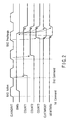
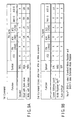
- FIG. 10 shows the pin allocation of a double-data-rate synchronous FCRAM (DDR-FCRAM) package some of whose control pins are used as address pins, as compared with the pin allocation of a DDR-SDRAM package.
- DDR-FCRAM double-data-rate synchronous FCRAM
- FIG. 10 shows the pin allocation of a double-data-rate synchronous FCRAM (DDR-FCRAM) package some of whose control pins are used as address pins, as compared with the pin allocation of a DDR-SDRAM package.
- DDR-FCRAM double-data-rate synchronous FCRAM
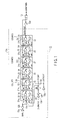
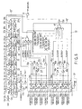
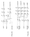
- the output terminal of the clocked inverter 124 controlled by signals CLKIN, bCLKIN is connected to the input terminal of the inverter 106.
- the input terminal of the clocked inverter 124 is connected to the output terminal of the inverter 106.
- the output terminal of the clocked inverter 126 controlled by signals bCLKIN, CLKIN is connected to the input terminal of the inverter 107.
- the input terminal of the clocked inverter 126 is connected to the output terminal of the inverter 107.
- the output terminal of the inverter 151 is connected to a first input terminal of the NAND gate 161.
- the output terminal of the inverter 154 is connected to a second input terminal of the NAND gate 161.
- the output terminal of the inverter 110 shown in FIG. 11 is connected to a third input terminal of the NAND gate 161. Then, a signal bACTUDSB is supplied from the output terminal of the inverter 110.
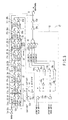
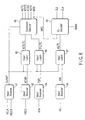
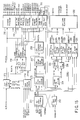
- the bit-line equalize circuits 313, 314 are each composed of equalize n-channel transistors 313a, 313b to which equalize internal potential VBLEQ! is applied and 314a, 314b and bit-line short n-channel transistors 313c, 314c, respectively.
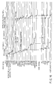
- test mode signal TMBKADJ ⁇ 2> changes to the high level or fuse signal bFSBKADJ ⁇ 2> changes to the low level
- the output DLYADJ ⁇ 2> of the NOR gate 46d becomes effective.
- the outputs of the inverters 45a to 45l inputted to the AND-to-NOR gate 47 become effective.
- the RAS restore time with 12 stages of delay in the inverters 45a to 451 is secured.
Landscapes
- Dram (AREA)
- For Increasing The Reliability Of Semiconductor Memories (AREA)
- Tests Of Electronic Circuits (AREA)
Applications Claiming Priority (4)
| Application Number | Priority Date | Filing Date | Title |
|---|---|---|---|
| JP2001284111 | 2001-09-18 | ||
| JP2001284111 | 2001-09-18 | ||
| JP2002251604 | 2002-08-29 | ||
| JP2002251604A JP4000028B2 (ja) | 2001-09-18 | 2002-08-29 | 同期型半導体記憶装置 |
Publications (3)
| Publication Number | Publication Date |
|---|---|
| EP1293984A2 true EP1293984A2 (de) | 2003-03-19 |
| EP1293984A3 EP1293984A3 (de) | 2004-10-27 |
| EP1293984B1 EP1293984B1 (de) | 2011-06-08 |
Family
ID=26622454
Family Applications (1)
| Application Number | Title | Priority Date | Filing Date |
|---|---|---|---|
| EP02020557A Expired - Lifetime EP1293984B1 (de) | 2001-09-18 | 2002-09-17 | Synchrone Halbleiterspeicheranordnung |
Country Status (5)
| Country | Link |
|---|---|
| US (1) | US6731559B2 (de) |
| EP (1) | EP1293984B1 (de) |
| JP (1) | JP4000028B2 (de) |
| KR (1) | KR100439923B1 (de) |
| CN (1) | CN1264219C (de) |
Families Citing this family (15)
| Publication number | Priority date | Publication date | Assignee | Title |
|---|---|---|---|---|
| JP3792602B2 (ja) * | 2002-05-29 | 2006-07-05 | エルピーダメモリ株式会社 | 半導体記憶装置 |
| JP2005141845A (ja) | 2003-11-07 | 2005-06-02 | Fujitsu Ltd | 半導体装置 |
| KR100642441B1 (ko) | 2004-04-19 | 2006-11-06 | 주식회사 하이닉스반도체 | 반도체 메모리 소자의 제어 회로 |
| KR100642414B1 (ko) | 2004-04-20 | 2006-11-03 | 주식회사 하이닉스반도체 | 반도체 메모리 소자의 제어 회로 |
| KR100612950B1 (ko) | 2004-04-22 | 2006-08-14 | 주식회사 하이닉스반도체 | 외부클럭을 사용한 디램의 라스타임 제어회로 및 라스타임제어방법 |
| KR100625293B1 (ko) * | 2004-06-30 | 2006-09-20 | 주식회사 하이닉스반도체 | 높은 신뢰성을 갖는 반도체메모리소자 및 그를 위한구동방법 |
| US7277982B2 (en) * | 2004-07-27 | 2007-10-02 | International Business Machines Corporation | DRAM access command queuing structure |
| JP2007200504A (ja) * | 2006-01-30 | 2007-08-09 | Fujitsu Ltd | 半導体メモリ、メモリコントローラ及び半導体メモリの制御方法 |
| US8700886B2 (en) * | 2007-05-30 | 2014-04-15 | Agere Systems Llc | Processor configured for operation with multiple operation codes per instruction |
| KR101124321B1 (ko) | 2010-04-06 | 2012-03-28 | 주식회사 하이닉스반도체 | 반도체 메모리 장치 및 그 리드/라이트 제어 방법 |
| KR101215647B1 (ko) * | 2011-01-28 | 2012-12-26 | 에스케이하이닉스 주식회사 | 반도체메모리장치 |
| JP5911834B2 (ja) * | 2013-09-11 | 2016-04-27 | 株式会社東芝 | 不揮発性半導体記憶装置 |
| JP6390683B2 (ja) * | 2016-09-28 | 2018-09-19 | ミツミ電機株式会社 | 半導体集積回路 |
| KR20180114712A (ko) * | 2017-04-11 | 2018-10-19 | 에스케이하이닉스 주식회사 | 리프레쉬 컨트롤러 및 그를 포함하는 반도체 메모리 장치 |
| KR102708728B1 (ko) * | 2019-01-15 | 2024-09-23 | 에스케이하이닉스 주식회사 | 반도체장치 및 반도체시스템 |
Family Cites Families (7)
| Publication number | Priority date | Publication date | Assignee | Title |
|---|---|---|---|---|
| IL96808A (en) * | 1990-04-18 | 1996-03-31 | Rambus Inc | Introductory / Origin Circuit Agreed Using High-Performance Brokerage |
| JP3843145B2 (ja) * | 1995-12-25 | 2006-11-08 | 株式会社ルネサステクノロジ | 同期型半導体記憶装置 |
| JP4043151B2 (ja) | 1998-08-26 | 2008-02-06 | 富士通株式会社 | 高速ランダムアクセス可能なメモリデバイス |
| JP2000163969A (ja) * | 1998-09-16 | 2000-06-16 | Fujitsu Ltd | 半導体記憶装置 |
| JP4050839B2 (ja) * | 1999-01-29 | 2008-02-20 | 松下電器産業株式会社 | 半導体記憶装置 |
| US6061285A (en) * | 1999-11-10 | 2000-05-09 | Mitsubishi Denki Kabushiki Kaisha | Semiconductor memory device capable of executing earlier command operation in test mode |
| JP4253097B2 (ja) | 1999-12-28 | 2009-04-08 | 東芝マイクロエレクトロニクス株式会社 | 半導体記憶装置及びそのデータ読み出し方法 |
-
2002
- 2002-08-29 JP JP2002251604A patent/JP4000028B2/ja not_active Expired - Fee Related
- 2002-09-17 US US10/244,962 patent/US6731559B2/en not_active Expired - Lifetime
- 2002-09-17 EP EP02020557A patent/EP1293984B1/de not_active Expired - Lifetime
- 2002-09-17 KR KR10-2002-0056351A patent/KR100439923B1/ko not_active Expired - Fee Related
- 2002-09-18 CN CNB021307415A patent/CN1264219C/zh not_active Expired - Fee Related
Also Published As
| Publication number | Publication date |
|---|---|
| EP1293984B1 (de) | 2011-06-08 |
| US6731559B2 (en) | 2004-05-04 |
| US20030053362A1 (en) | 2003-03-20 |
| KR100439923B1 (ko) | 2004-07-12 |
| JP4000028B2 (ja) | 2007-10-31 |
| KR20030024617A (ko) | 2003-03-26 |
| EP1293984A3 (de) | 2004-10-27 |
| JP2003168292A (ja) | 2003-06-13 |
| CN1405889A (zh) | 2003-03-26 |
| CN1264219C (zh) | 2006-07-12 |
Similar Documents
| Publication | Publication Date | Title |
|---|---|---|
| US6233192B1 (en) | Semiconductor memory device | |
| US7057950B2 (en) | Semiconductor memory devices with delayed auto-precharge function and associated methods of auto-precharging semiconductor memory devices | |
| US6522600B2 (en) | Fast cycle RAM and data readout method therefor | |
| US6795370B2 (en) | Fast cycle RAM having improved data write operation | |
| US6134169A (en) | Semiconductor memory device | |
| US5715203A (en) | Semiconductor memory device and automatic bit line precharge method therefor | |
| EP1293984B1 (de) | Synchrone Halbleiterspeicheranordnung | |
| JP2002343100A (ja) | プリチャージ制御信号生成回路及びこれを用いた半導体メモリ装置 | |
| US6529423B1 (en) | Internal clock signal delay circuit and method for delaying internal clock signal in semiconductor device | |
| JP2022144926A (ja) | 半導体メモリ装置 | |
| US6636443B2 (en) | Semiconductor memory device having row buffers | |
| US6789137B2 (en) | Semiconductor memory device allowing reduction of I/O terminals | |
| US6166993A (en) | Synchronous semiconductor memory device | |
| US6456563B1 (en) | Semiconductor memory device that operates in sychronization with a clock signal | |
| US6862244B2 (en) | DRAM with segmental cell arrays and method of accessing same | |
| US5703829A (en) | Synchronous type semiconductor memory device which can be adapted to high frequency system clock signal | |
| KR100405582B1 (ko) | 동기형 반도체 기억 장치 | |
| US6310825B1 (en) | Data writing method for semiconductor memory device | |
| US20080247261A1 (en) | Semiconductor memory device and control method thereof | |
| US5663912A (en) | Semiconductor memory device | |
| JP3746319B2 (ja) | 半導体記憶装置 | |
| Pawlowski | Memory Performance Tutorial Hot Chips 16 | |
| GB2407422A (en) | Semiconductor memory device |
Legal Events
| Date | Code | Title | Description |
|---|---|---|---|
| PUAI | Public reference made under article 153(3) epc to a published international application that has entered the european phase |
Free format text: ORIGINAL CODE: 0009012 |
|
| 17P | Request for examination filed |
Effective date: 20020917 |
|
| AK | Designated contracting states |
Kind code of ref document: A2 Designated state(s): AT BE BG CH CY CZ DE DK EE ES FI FR GB GR IE IT LI LU MC NL PT SE SK TR |
|
| AX | Request for extension of the european patent |
Extension state: AL LT LV MK RO SI |
|
| PUAL | Search report despatched |
Free format text: ORIGINAL CODE: 0009013 |
|
| AK | Designated contracting states |
Kind code of ref document: A3 Designated state(s): AT BE BG CH CY CZ DE DK EE ES FI FR GB GR IE IT LI LU MC NL PT SE SK TR |
|
| AX | Request for extension of the european patent |
Extension state: AL LT LV MK RO SI |
|
| AKX | Designation fees paid |
Designated state(s): DE FR GB |
|
| 17Q | First examination report despatched |
Effective date: 20071129 |
|
| GRAP | Despatch of communication of intention to grant a patent |
Free format text: ORIGINAL CODE: EPIDOSNIGR1 |
|
| GRAS | Grant fee paid |
Free format text: ORIGINAL CODE: EPIDOSNIGR3 |
|
| GRAA | (expected) grant |
Free format text: ORIGINAL CODE: 0009210 |
|
| AK | Designated contracting states |
Kind code of ref document: B1 Designated state(s): DE FR GB |
|
| REG | Reference to a national code |
Ref country code: GB Ref legal event code: FG4D |
|
| REG | Reference to a national code |
Ref country code: DE Ref legal event code: R096 Ref document number: 60240218 Country of ref document: DE Effective date: 20110721 |
|
| PLBE | No opposition filed within time limit |
Free format text: ORIGINAL CODE: 0009261 |
|
| STAA | Information on the status of an ep patent application or granted ep patent |
Free format text: STATUS: NO OPPOSITION FILED WITHIN TIME LIMIT |
|
| 26N | No opposition filed |
Effective date: 20120309 |
|
| REG | Reference to a national code |
Ref country code: DE Ref legal event code: R097 Ref document number: 60240218 Country of ref document: DE Effective date: 20120309 |
|
| PGFP | Annual fee paid to national office [announced via postgrant information from national office to epo] |
Ref country code: DE Payment date: 20130911 Year of fee payment: 12 |
|
| PGFP | Annual fee paid to national office [announced via postgrant information from national office to epo] |
Ref country code: GB Payment date: 20130911 Year of fee payment: 12 Ref country code: FR Payment date: 20130910 Year of fee payment: 12 |
|
| REG | Reference to a national code |
Ref country code: DE Ref legal event code: R119 Ref document number: 60240218 Country of ref document: DE |
|
| GBPC | Gb: european patent ceased through non-payment of renewal fee |
Effective date: 20140917 |
|
| REG | Reference to a national code |
Ref country code: FR Ref legal event code: ST Effective date: 20150529 |
|
| PG25 | Lapsed in a contracting state [announced via postgrant information from national office to epo] |
Ref country code: DE Free format text: LAPSE BECAUSE OF NON-PAYMENT OF DUE FEES Effective date: 20150401 Ref country code: GB Free format text: LAPSE BECAUSE OF NON-PAYMENT OF DUE FEES Effective date: 20140917 |
|
| PG25 | Lapsed in a contracting state [announced via postgrant information from national office to epo] |
Ref country code: FR Free format text: LAPSE BECAUSE OF NON-PAYMENT OF DUE FEES Effective date: 20140930 |