EP1290800B1 - Digitaler phasenregelkreis - Google Patents
Digitaler phasenregelkreis Download PDFInfo
- Publication number
- EP1290800B1 EP1290800B1 EP01929630A EP01929630A EP1290800B1 EP 1290800 B1 EP1290800 B1 EP 1290800B1 EP 01929630 A EP01929630 A EP 01929630A EP 01929630 A EP01929630 A EP 01929630A EP 1290800 B1 EP1290800 B1 EP 1290800B1
- Authority
- EP
- European Patent Office
- Prior art keywords
- digital
- phase
- pulse
- controlled oscillator
- output
- Prior art date
- Legal status (The legal status is an assumption and is not a legal conclusion. Google has not performed a legal analysis and makes no representation as to the accuracy of the status listed.)
- Expired - Lifetime
Links
Images


Classifications
-
- H—ELECTRICITY
- H03—ELECTRONIC CIRCUITRY
- H03L—AUTOMATIC CONTROL, STARTING, SYNCHRONISATION, OR STABILISATION OF GENERATORS OF ELECTRONIC OSCILLATIONS OR PULSES
- H03L7/00—Automatic control of frequency or phase; Synchronisation
- H03L7/06—Automatic control of frequency or phase; Synchronisation using a reference signal applied to a frequency- or phase-locked loop
- H03L7/08—Details of the phase-locked loop
- H03L7/099—Details of the phase-locked loop concerning mainly the controlled oscillator of the loop
- H03L7/0991—Details of the phase-locked loop concerning mainly the controlled oscillator of the loop the oscillator being a digital oscillator, e.g. composed of a fixed oscillator followed by a variable frequency divider
-
- H—ELECTRICITY
- H03—ELECTRONIC CIRCUITRY
- H03L—AUTOMATIC CONTROL, STARTING, SYNCHRONISATION, OR STABILISATION OF GENERATORS OF ELECTRONIC OSCILLATIONS OR PULSES
- H03L7/00—Automatic control of frequency or phase; Synchronisation
- H03L7/06—Automatic control of frequency or phase; Synchronisation using a reference signal applied to a frequency- or phase-locked loop
- H03L7/08—Details of the phase-locked loop
- H03L7/085—Details of the phase-locked loop concerning mainly the frequency- or phase-detection arrangement including the filtering or amplification of its output signal
-
- H—ELECTRICITY
- H03—ELECTRONIC CIRCUITRY
- H03L—AUTOMATIC CONTROL, STARTING, SYNCHRONISATION, OR STABILISATION OF GENERATORS OF ELECTRONIC OSCILLATIONS OR PULSES
- H03L7/00—Automatic control of frequency or phase; Synchronisation
- H03L7/06—Automatic control of frequency or phase; Synchronisation using a reference signal applied to a frequency- or phase-locked loop
- H03L7/16—Indirect frequency synthesis, i.e. generating a desired one of a number of predetermined frequencies using a frequency- or phase-locked loop
- H03L7/18—Indirect frequency synthesis, i.e. generating a desired one of a number of predetermined frequencies using a frequency- or phase-locked loop using a frequency divider or counter in the loop
-
- H—ELECTRICITY
- H03—ELECTRONIC CIRCUITRY
- H03L—AUTOMATIC CONTROL, STARTING, SYNCHRONISATION, OR STABILISATION OF GENERATORS OF ELECTRONIC OSCILLATIONS OR PULSES
- H03L2207/00—Indexing scheme relating to automatic control of frequency or phase and to synchronisation
- H03L2207/50—All digital phase-locked loop
-
- H—ELECTRICITY
- H03—ELECTRONIC CIRCUITRY
- H03L—AUTOMATIC CONTROL, STARTING, SYNCHRONISATION, OR STABILISATION OF GENERATORS OF ELECTRONIC OSCILLATIONS OR PULSES
- H03L7/00—Automatic control of frequency or phase; Synchronisation
- H03L7/06—Automatic control of frequency or phase; Synchronisation using a reference signal applied to a frequency- or phase-locked loop
- H03L7/08—Details of the phase-locked loop
- H03L7/085—Details of the phase-locked loop concerning mainly the frequency- or phase-detection arrangement including the filtering or amplification of its output signal
- H03L7/089—Details of the phase-locked loop concerning mainly the frequency- or phase-detection arrangement including the filtering or amplification of its output signal the phase or frequency detector generating up-down pulses
-
- H—ELECTRICITY
- H03—ELECTRONIC CIRCUITRY
- H03L—AUTOMATIC CONTROL, STARTING, SYNCHRONISATION, OR STABILISATION OF GENERATORS OF ELECTRONIC OSCILLATIONS OR PULSES
- H03L7/00—Automatic control of frequency or phase; Synchronisation
- H03L7/06—Automatic control of frequency or phase; Synchronisation using a reference signal applied to a frequency- or phase-locked loop
- H03L7/08—Details of the phase-locked loop
- H03L7/085—Details of the phase-locked loop concerning mainly the frequency- or phase-detection arrangement including the filtering or amplification of its output signal
- H03L7/091—Details of the phase-locked loop concerning mainly the frequency- or phase-detection arrangement including the filtering or amplification of its output signal the phase or frequency detector using a sampling device
Definitions
- the present invention relates to a phase locked loop according to the preamble of claim 1, as from US 5,727,038 known.
- phase locked loop which a Phase detector, a digital loop filter, a digital having a controlled oscillator and a divider circuit, related to a signal having a fixed predetermined phase to generate a reference signal.
- a phase detector generates a first control signal in response to the phase relationship between the reference signal and a feedback one Signal.
- the digital filter receives the first control signal and generates from this a second control signal, wherein the second control signal is present in digital form.
- the digital controlled oscillator processes this second control signal, so that he has a frequency corresponding to the second one Outputs control signal.
- a phase error detector generates a phase error signal, whose width corresponds to the magnitude of the phase error.
- a pulse width detector quantizes the pulse width. Of the quantized value is stored in a buffer. The buffer becomes the last quantized value loaded and compared with the current by a comparator. The comparator gives according to a change of the Phase error signal a control signal to a digitally controlled Oscillator.
- From US-A-6,005,427 is a digital phase locked loop with a phase detector for detecting the analog phase difference between an input signal and an output signal a digitally controlled oscillator, wherein the digital Output signal of the phase detector a digital Loop filter is supplied, the output signal then the digitally controlled oscillator to adjust its Output clock is supplied.
- US-A-6,052,034 and US-A-6,028,488 disclose digital Phase locked loops, where a digital loop filter is used.
- phase locked loop To generate frequencies that are at a specific reference frequency are synchronized, is the use of analog Phase locked loop (PLL) known.
- PLL Phase locked loop
- Such an analog phase locked loop is for example from the document F.M. Gardner, "Charge-Pump Phase-Locked Loops, "IEEE Trans. Comm., Vol. 28, pp. 1849-1858, November 1980 known.
- This analog phase locked loop comprises a phase / frequency detector ("Phase / Frequency Detector", PFD), the the output clock of a voltage controlled oscillator (“Voltage Controlled Oscillator ", VCO) compares with a reference clock and generates as output voltage pulses, which the information of the phase and frequency difference between the output clock of the voltage controlled oscillator and the reference clock.
- PFD phase / frequency detector
- VCO Voltage Controlled Oscillator
- the voltage pulses are a charge pump which supplies the voltage pulses in converts corresponding current pulses, these current pulses in turn from a transimpedance loop filter first or higher order.
- the voltage controlled Oscillator will eventually by the output of the Loop filter energized according to its output tact adjust.
- a divider may be arranged so that the phase / frequency detector the output clock of the voltage controlled oscillator divided by a factor N, where N is any one positive number can be. In the adjusted condition the phase locked loop thus corresponds to the output frequency of the voltage-controlled oscillator of the N-fold reference frequency.
- the present invention is therefore based on the object a digital phase locked loop with a digitally controlled Oscillator to propose the use of any digital loop filter allows, so that the developer always the most suitable for the respective application Transfer function can choose.
- the phase detector device should be timed concentrated phase difference information into one about the Timeline distributed phase information in the form of a numeric digital value, which then has to be adapted to Way integrated in the digital loop filter can be.
- Phase locked loop is a phase / frequency analog / digital converter ("Phase / Frequency Analog to Digital Converter ", the PFDC), which compares the by comparison Output clock of the digitally controlled oscillator with the reference clock obtained phase and frequency information such quantized that they are no longer as with conventional analogue Charge pump phase locked loops in short current or Voltage pulses is concentrated, but in a digital Control value implemented and evenly along the time axis is distributed. For this, the digital manipulated variable is in an output register output. The value in the output register remains until a new phase error is quantized has been.
- the advantage of this solution is that the Charge pump is eliminated and the analog loop filter replaces any type of digital loop filter becomes.
- a loop filter may be an IIR filter FIR filter, a wave digital filter or a bilinear Transformation filters, etc. are used.
- one or more frequency dividers can be arranged. As well can be the reference frequency through one or more frequency divider be divided before they of the invention Phase detector means is supplied.
- the reference clock f.sub.ref is divided down by the frequency divider 6 with the divider factor 1 / M and then supplied as an input signal I1 to the phase detector device 1.
- the phase detector device 1 receives, as another input signal 12, the output clock f of the digitally controlled oscillator 3 previously divided by the frequency dividers 4 and 5 with the divider factors 1 / N and 1 / M.
- the phase detector device 1 detects the phase difference between the two input signals I1 and I2. It quantizes them in a suitable manner and thus converts the phase difference into a numerical digital control value, which is supplied to the digital loop filter 2 via a bus with a suitable bus width n SA .
- FIG. 5 also shows a circuit part with an absolute value image 18, a logical NOT element 19, a register 20, a logical AND gate 21 and a logical OR gate 22 shown, wherein the AND gate 21 whenever a Udl pulse is over, a reset pulse is generated and sent to a Reset input of the up / down counter 16 applies to the Reset counter reading to zero. Furthermore, will via the output of the OR gate 22 after each Ud1 pulse Enable pulse to a release terminal of an output register 17 so that the final result of the up / down counter 16 is output as the output value. This output value is retained until a new one Udl pulse occurs.
Description
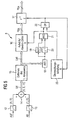
- Figur 1
- zeigt ein vereinfachtes Blockschaltbild eines digitalen Phasenregelkreises gemäß einem bevorzugten Ausführungsbeispiel der vorliegenden Erfindung,
- Figur 2
- zeigt den Aufbau einer in Figur 1 gezeigten Phasendetektoreinrichtung,
- Figur 3
- zeigt eine Darstellung zur Verdeutlichung der Funktionsweise der in Figur 1 und Figur 2 gezeigten Phasendetektoreinrichtung,
- Figur 4
- zeigt den Aufbau eines in Figur 2 gezeigten Flankendetektors, und
- Figur 5
- zeigt den Aufbau eines in Figur 2 gezeigten Quantisierers.
Claims (7)
- Digitaler Phasenregelkreis,
mit einem digital gesteuerten Oszillator (3) zur Erzeugung eines bestimmten Ausgabetakts (f),
mit einer Phasendetektoreinrichtung (1) zum Erfassen der analogen Phasendifferenz zwischen einem von dem Ausgabetakt (f) des digital gesteuerten Oszillators (3) abhängigen Takt und
einem Referenztakt (fref) und zum Umsetzen der erfaßten analogen Phasendifferenz in einen entsprechenden digitalen Stellwert für den digital gesteuerten Oszillator (3), und
mit einem digitalen Schleifenfilter (2), über welches der digitale Stellwert der Phasendetektoreinrichtung (1) dem digital gesteuerten Oszillator (3) zur Einstellung seines Ausgabetakts (f) zugeführt ist,
wobei die Phasendetektoreinrichtung (1) einen Phasendetektor (24) und eine Quantisiereinrichtung (8) umfaßt,
wobei der Phasendetektor (24) in Abhängigkeit von der Phasendifferenz ein erstes Impulssignal (AUF) und ein zweites Impulssignal (AB) erzeugt, wobei ein Impuls des ersten Impulssignals (AUF) erzeugt wird, wenn der von dem Ausgabetakt (f) des digital gesteuerten Oszillators (3) abhängige Takt kleiner als der Referenztakt (fref) ist, während ein Impuls des zweiten Impulssignals (AB) erzeugt wird, wenn der von dem Ausgabetakt (f) des digital gesteuerten Oszillators (3) abhängige Takt größer als der Referenztakt (fref) ist, und
wobei die Quantisiereinrichtung (8) einen ersten Schaltungsabschnitt (12-14) zum Abtasten des ersten und zweiten Impulssignals (AUF, AB) und zum Subtrahieren der somit gewonnenen Abtastwerte des ersten und zweiten Impulssignals (AUF, AB) aufweist, um somit einen entsprechenden digitalen Differenzwert (Ud) zu erzeugen, und
daß die Quantisiereinrichtung (8) einen Zähler (16) aufweist, dessen Zählerstand in Abhängigkeit von dem jeweils erzeugten digitalen Differenzwert (Ud) des ersten Schaltungsabschnitts (12-14) verändert wird, wobei der Zählerstand des Zählers (16) als Grundlage für den digitalen Stellwert dient,
dadurch gekennzeichnet, daß die Quantisiereinrichtung (8) einen zweiten Schaltungsabschnitt (18-22) aufweist, der derart ausgestaltet ist, daß das von dem ersten Schaltungsabschnitt (12-14) erzeugte digitale Differenzwertsignal auf das Ende eines Impulses hin überwacht wird und in diesem Fall ein Rücksetzsignal für den Zähler (16) zum Zurücksetzen dessen Zählerstands erzeugt wird, und
daß die Quantisiereinrichtung (8) ein Ausgaberegister (17) aufweist, über welches der augenblickliche Zählerstand des Zählers (16) ausgegeben wird, wobei das Ausgaberegister (17) bei Vorliegen des Rücksetzsignals des zweiten Schaltungsabschnitts (18-22) aktiviert wird. - Digitaler Phasenregelkreis nach Anspruch 1,
dadurch gekennzeichnet, daß der Ausgabetakt (f) des digital gesteuerten Oszillators (3) der Phasendetektoreinrichtung (1) über mindestens einen Frequenzteiler (4, 5) zugeführt ist. - Digitaler Phasenregelkreis nach Anspruch 1 oder 2,
dadurch gekennzeichnet, daß der Referenztakt (fref) der Phasendetektoreinrichtung (1) über mindestens einen Frequenzteiler (6) zugeführt ist. - Digitaler Phasenregelkreis nach einem der vorhergehenden Ansprüche,
dadurch gekennzeichnet, daß der digital gesteuerte Oszillator (3) als Quarzoszillator ausgestaltet ist. - Digitaler Phasenregelkreis nach Anspruch 1,
dadurch gekennzeichnet, daß die Quantisiereinrichtung (8) einen dritten Schaltungsabschnitt (23) aufweist, der derart ausgestaltet ist, daß er feststellt, wenn das von dem ersten Schaltungsabschnitt (12-14) erzeugte digitale Differenzwertsignal (Ud) keine Impulse aufweist und in diesem Fall den von dem Ausgaberegister (17) ausgegebenen letzten digitalen Wert durch den Wert Null ersetzt. - Digitaler Phasenregelkreis nach einem der vorhergehenden Ansprüche,
dadurch gekennzeichnet, daß die Phasendetektoreinrichtung (1) eine Pulsdetektoreinrichtung (7) und eine Addiereinrichtung (9) umfaßt,
wobei die Pulsdetektoreinrichtung (7) derart ausgestaltet ist, daß sie das Auftreten von Pulsen des ersten Impulssignals (AUF) und des zweiten Impulssignals (AB) überwacht und
abhängig davon, ob ein Puls in dem ersten Impulssignal (AUF) oder dem zweiten Impulssignal (AB) auftritt, einen digitalen Korrekturwert erzeugt, und
wobei der digitale Korrekturwert der Pulsdetektoreinrichtung (7) und der digitale Ausgabewert der Quantisiereinrichtung (8) der Addiereinrichtung (9) zur Addition zugeführt ist, so daß die Addiereinrichtung (9) den daraus resultierenden digitalen Summenwert als den digitalen Stellwert dem digitalen Schleifenfilter (2) zuführt. - Digitaler Phasenregelkreis nach Anspruch 6,
dadurch gekennzeichnet, daß die Pulsdetektoreinrichtung (7) der Phasendetektoreinrichtung (1) derart ausgestaltet ist, daß sie den digitalen Korrekturwert in Form eines Impulssignals mit programmierbarer Pulslänge erzeugt.
Applications Claiming Priority (3)
| Application Number | Priority Date | Filing Date | Title |
|---|---|---|---|
| DE10022486A DE10022486C1 (de) | 2000-05-09 | 2000-05-09 | Digitaler Phasenregelkreis |
| DE10022486 | 2000-05-09 | ||
| PCT/EP2001/005227 WO2001086816A1 (de) | 2000-05-09 | 2001-05-08 | Digitaler phasenregelkreis |
Publications (2)
| Publication Number | Publication Date |
|---|---|
| EP1290800A1 EP1290800A1 (de) | 2003-03-12 |
| EP1290800B1 true EP1290800B1 (de) | 2005-02-16 |
Family
ID=7641260
Family Applications (1)
| Application Number | Title | Priority Date | Filing Date |
|---|---|---|---|
| EP01929630A Expired - Lifetime EP1290800B1 (de) | 2000-05-09 | 2001-05-08 | Digitaler phasenregelkreis |
Country Status (5)
| Country | Link |
|---|---|
| US (1) | US6970046B2 (de) |
| EP (1) | EP1290800B1 (de) |
| CN (1) | CN1398455A (de) |
| DE (2) | DE10022486C1 (de) |
| WO (1) | WO2001086816A1 (de) |
Families Citing this family (39)
| Publication number | Priority date | Publication date | Assignee | Title |
|---|---|---|---|---|
| DE60209774T2 (de) * | 2001-11-30 | 2006-11-02 | Koninklijke Philips Electronics N.V. | Bitdetektionsanordnung und vorrichtung zur wiedergabe von informationen |
| DE10219857B4 (de) * | 2002-05-03 | 2006-01-05 | Infineon Technologies Ag | PLL-Schaltung und Verfahren zur Eliminierung von Eigenjitter eines von einer Regelungsschaltung empfangenen Signals |
| US8306176B2 (en) * | 2002-06-19 | 2012-11-06 | Texas Instruments Incorporated | Fine-grained gear-shifting of a digital phase-locked loop (PLL) |
| US6838912B1 (en) * | 2003-07-01 | 2005-01-04 | Realtek Semiconductor Corp. | Digital fractional phase detector |
| US7463310B2 (en) * | 2003-08-14 | 2008-12-09 | Broadcom Corporation | BTSC pilot signal lock |
| JP3803805B2 (ja) * | 2003-09-05 | 2006-08-02 | 日本テキサス・インスツルメンツ株式会社 | ディジタル位相同期ループ回路 |
| DE102004006995B4 (de) * | 2004-02-12 | 2007-05-31 | Infineon Technologies Ag | Digitaler Phasenregelkreis für Sub-µ-Technologien |
| DE102004037162A1 (de) | 2004-07-30 | 2006-03-23 | Infineon Technologies Ag | Verfahren und Vorrichtung zur Erzeugung eines Taktsignals |
| CN1741389B (zh) * | 2004-08-26 | 2014-06-11 | 瑞昱半导体股份有限公司 | 具有非线性相位误差反应特性的锁相环 |
| FR2875972B1 (fr) * | 2004-09-30 | 2006-12-15 | St Microelectronics Sa | Synthetiseur de frequence a pll |
| CN100446422C (zh) * | 2005-01-06 | 2008-12-24 | 华为技术有限公司 | 锁相环失效检测方法 |
| CN1815892B (zh) * | 2005-01-31 | 2011-09-28 | 瑞昱半导体股份有限公司 | 一种检测相位误差并产生控制信号的电路 |
| US7248122B2 (en) * | 2005-09-14 | 2007-07-24 | Fairchild Semiconductor Corporation | Method and apparatus for generating a serial clock without a PLL |
| US7680227B2 (en) * | 2006-03-02 | 2010-03-16 | Broadcom Corporation | Method and system for filter calibration using fractional-N frequency synthesized signals |
| US7355462B1 (en) * | 2006-07-10 | 2008-04-08 | Altera Corporation | Phase lock loop and method for operating the same |
| EP1903681B1 (de) | 2006-09-21 | 2009-07-22 | Siemens Aktiengesellschaft | Verfahren zur Taktsynchronisation eines elektrischen Geräts auf einen Referenztakt und elektrisches Gerät |
| US7859343B2 (en) * | 2006-11-13 | 2010-12-28 | Industrial Technology Research Institute | High-resolution varactors, single-edge triggered digitally controlled oscillators, and all-digital phase-locked loops using the same |
| GB0622948D0 (en) * | 2006-11-17 | 2006-12-27 | Zarlink Semiconductor Inc | A digital phase locked loop |
| US7656236B2 (en) * | 2007-05-15 | 2010-02-02 | Teledyne Wireless, Llc | Noise canceling technique for frequency synthesizer |
| US20080316081A1 (en) * | 2007-06-21 | 2008-12-25 | Favepc, Inc. | Battery-free remote control device |
| US7786771B2 (en) * | 2008-05-27 | 2010-08-31 | Taiwan Semiconductor Manufacturing Company, Ltd. | Phase lock loop (PLL) with gain control |
| US7847646B2 (en) * | 2008-05-27 | 2010-12-07 | Favepc, Inc. | Carrier generator with LC network |
| CN101594146B (zh) * | 2008-05-29 | 2011-08-24 | 中芯国际集成电路制造(北京)有限公司 | 锁相环电路 |
| CN101594147B (zh) * | 2008-05-29 | 2011-08-24 | 中芯国际集成电路制造(北京)有限公司 | 锁相环电路 |
| US8102195B2 (en) * | 2009-05-13 | 2012-01-24 | Mediatek Inc. | Digital phase-locked loop circuit including a phase delay quantizer and method of use |
| US8553827B2 (en) * | 2009-10-20 | 2013-10-08 | Qualcomm Incorporated | ADC-based mixed-mode digital phase-locked loop |
| TWI478500B (zh) * | 2009-09-23 | 2015-03-21 | Richwave Technology Corp | 數位鎖相迴路、頻率調整方法和整合式接收器 |
| CN101694998B (zh) * | 2009-10-23 | 2014-12-31 | 中兴通讯股份有限公司 | 一种锁定系统及方法 |
| JP2011188183A (ja) * | 2010-03-08 | 2011-09-22 | Sony Corp | 位相同期ループ回路、半導体集積回路、電子機器、位相同期ループ回路の制御方法 |
| US8862648B2 (en) | 2011-05-24 | 2014-10-14 | Taiwan Semiconductor Manufacturing Company, Ltd. | Fast filter calibration apparatus |
| US9214945B2 (en) | 2012-02-27 | 2015-12-15 | Realtek Semiconductor Corp. | Digital phase lock loop and method thereof |
| US8890592B2 (en) * | 2012-10-13 | 2014-11-18 | Infineon Technologies Ag | Multi-output phase detector |
| US10007639B2 (en) * | 2015-04-08 | 2018-06-26 | Microsemi Semiconductor Ulc | PLL system with master and slave devices |
| US9425808B1 (en) * | 2015-06-05 | 2016-08-23 | Texas Instruments Incorporated | Frequency detector |
| CN107342767B (zh) * | 2017-07-07 | 2020-07-28 | 广东中星微电子有限公司 | 判断锁相环锁定状态的方法和装置 |
| US10727745B2 (en) | 2017-07-25 | 2020-07-28 | Kinetic Technologies | Systems and methods for providing intelligent constant on-time control |
| US20190238144A1 (en) * | 2018-01-31 | 2019-08-01 | Integrated Device Technology, Inc. | ADC Based PLL |
| CN111641402B (zh) * | 2020-06-23 | 2023-07-14 | 湖南国科微电子股份有限公司 | 一种数字环路滤波电路及其带宽调整方法 |
| CN114499511B (zh) * | 2022-01-14 | 2023-03-28 | 中星联华科技(北京)有限公司 | 适用于码型发生器的抖动信号注入装置、系统及方法 |
Family Cites Families (11)
| Publication number | Priority date | Publication date | Assignee | Title |
|---|---|---|---|---|
| US5258724A (en) | 1983-12-30 | 1993-11-02 | Itt Corporation | Frequency synthesizer |
| US4577163A (en) * | 1984-07-09 | 1986-03-18 | Honeywell Inc. | Digital phase locked loop |
| US5077529A (en) * | 1989-07-19 | 1991-12-31 | Level One Communications, Inc. | Wide bandwidth digital phase locked loop with reduced low frequency intrinsic jitter |
| EP0758171A3 (de) * | 1995-08-09 | 1997-11-26 | Symbios Logic Inc. | Datenabtastung und -rückgewinnung |
| JP3141760B2 (ja) * | 1995-12-06 | 2001-03-05 | ヤマハ株式会社 | デジタルpll回路 |
| US5739725A (en) * | 1996-01-29 | 1998-04-14 | International Business Machines Corporation | Digitally controlled oscillator circuit |
| US5727038A (en) | 1996-09-06 | 1998-03-10 | Motorola, Inc. | Phase locked loop using digital loop filter and digitally controlled oscillator |
| US6028488A (en) * | 1996-11-08 | 2000-02-22 | Texas Instruments Incorporated | Digitally-controlled oscillator with switched-capacitor frequency selection |
| US6005425A (en) * | 1998-02-04 | 1999-12-21 | Via-Cyrix Inc. | PLL using pulse width detection for frequency and phase error correction |
| US6052034A (en) * | 1998-06-24 | 2000-04-18 | Industrial Technology Research Institute | Method and apparatus for all digital holdover circuit |
| US6664827B2 (en) * | 2001-03-02 | 2003-12-16 | Adc Telecommunications, Inc. | Direct digital synthesizer phase locked loop |
-
2000
- 2000-05-09 DE DE10022486A patent/DE10022486C1/de not_active Expired - Lifetime
-
2001
- 2001-05-08 WO PCT/EP2001/005227 patent/WO2001086816A1/de active IP Right Grant
- 2001-05-08 DE DE50105372T patent/DE50105372D1/de not_active Expired - Lifetime
- 2001-05-08 US US10/275,826 patent/US6970046B2/en not_active Expired - Fee Related
- 2001-05-08 CN CN01804819A patent/CN1398455A/zh active Pending
- 2001-05-08 EP EP01929630A patent/EP1290800B1/de not_active Expired - Lifetime
Also Published As
| Publication number | Publication date |
|---|---|
| EP1290800A1 (de) | 2003-03-12 |
| US6970046B2 (en) | 2005-11-29 |
| US20050077969A1 (en) | 2005-04-14 |
| CN1398455A (zh) | 2003-02-19 |
| DE10022486C1 (de) | 2002-01-17 |
| DE50105372D1 (de) | 2005-03-24 |
| WO2001086816A1 (de) | 2001-11-15 |
Similar Documents
| Publication | Publication Date | Title |
|---|---|---|
| EP1290800B1 (de) | Digitaler phasenregelkreis | |
| DE60036426T2 (de) | Direkte digitale Frequenzsynthese, die Störbeseitigung ermöglicht | |
| DE602004011277T2 (de) | Typ II komplett digitaler Phasenregelkreis | |
| DE10164916B4 (de) | Datenrückgewinnungsschaltungsanordnung | |
| DE10253879B4 (de) | Phasendetektor und Verfahren zur Taktsignal-Phasendifferenzkompensation | |
| DE102008008050B4 (de) | Auf digitaler Verzögerungsleitung basierender Frequenz-Synthesizer | |
| DE4125387A1 (de) | Verfahren und generatorschaltung zur analogen zeitsteuerung | |
| DE2645638C2 (de) | Phasendetektor in einer phasenstarren Schleife | |
| DE112009000483T5 (de) | Phasenregelkreis | |
| DE60031737T2 (de) | Frequenzregelkreis | |
| DE112009000512T5 (de) | Phasenregelkreis | |
| DE112014006322T5 (de) | Ladungspumpen-Kalibrierung für eine Zweiwege-Phasenregelungsschleife | |
| DE102006024471A1 (de) | Umschaltbarer Phasenregelkreis sowie Verfahren zum Betrieb eines umschaltbaren Phasenregelkreises | |
| DE19910885C2 (de) | Schaltungsanordnung zum störungsfreien Initialisieren von Delay-Locked-Loop-Schaltungen mit Fast-Lock | |
| DE102006024469B3 (de) | Phasenregelkreis zur Erzeugung mehrerer Ausgangssignale | |
| DE102006024470B4 (de) | Umschaltbarer Phasenregelkreis sowie Verfahren zum Betrieb eines umschaltbaren Phasenregelkreises | |
| DE60314085T2 (de) | System und Verfahren zur Beseitigung des Verstärkungsfehlers eines Phasendetektors bei der Taktrückgewinnung verursacht durch eine datenabhängig variierende Anzahl von Flankenwechseln | |
| EP0590323B1 (de) | Filter zur Einstellung der Bandbreite eines Regelkreises | |
| EP1525662B1 (de) | Digital gesteuerter oszillator | |
| DE3938886A1 (de) | Digitaler phasenregelkreis | |
| DE4135630C2 (de) | Digitaler Impulsgenerator | |
| DE69832674T2 (de) | Phasenregelkreis und Verfahren zur Rückgewinnung eines Taktsignals | |
| EP1573921A1 (de) | Digital steuerbarer oszillator | |
| WO2005078935A1 (de) | Digitaler phasenregelkreis mit schnellem einschwingverhalten | |
| DE102009052481B4 (de) | Phasenregelkreis |
Legal Events
| Date | Code | Title | Description |
|---|---|---|---|
| PUAI | Public reference made under article 153(3) epc to a published international application that has entered the european phase |
Free format text: ORIGINAL CODE: 0009012 |
|
| 17P | Request for examination filed |
Effective date: 20020524 |
|
| AK | Designated contracting states |
Kind code of ref document: A1 Designated state(s): AT BE CH CY DE DK ES FI FR GB GR IE IT LI LU MC NL PT SE TR |
|
| AX | Request for extension of the european patent |
Extension state: AL LT LV MK RO SI |
|
| RBV | Designated contracting states (corrected) |
Designated state(s): AT BE CH DE FR GB LI |
|
| 17Q | First examination report despatched |
Effective date: 20040504 |
|
| GRAP | Despatch of communication of intention to grant a patent |
Free format text: ORIGINAL CODE: EPIDOSNIGR1 |
|
| GRAP | Despatch of communication of intention to grant a patent |
Free format text: ORIGINAL CODE: EPIDOSNIGR1 |
|
| RBV | Designated contracting states (corrected) |
Designated state(s): DE FR GB |
|
| GRAS | Grant fee paid |
Free format text: ORIGINAL CODE: EPIDOSNIGR3 |
|
| GRAA | (expected) grant |
Free format text: ORIGINAL CODE: 0009210 |
|
| AK | Designated contracting states |
Kind code of ref document: B1 Designated state(s): DE FR GB |
|
| PG25 | Lapsed in a contracting state [announced via postgrant information from national office to epo] |
Ref country code: GB Free format text: LAPSE BECAUSE OF FAILURE TO SUBMIT A TRANSLATION OF THE DESCRIPTION OR TO PAY THE FEE WITHIN THE PRESCRIBED TIME-LIMIT Effective date: 20050216 |
|
| REG | Reference to a national code |
Ref country code: GB Ref legal event code: FG4D Free format text: NOT ENGLISH |
|
| REG | Reference to a national code |
Ref country code: IE Ref legal event code: FG4D Free format text: GERMAN |
|
| REF | Corresponds to: |
Ref document number: 50105372 Country of ref document: DE Date of ref document: 20050324 Kind code of ref document: P |
|
| GBV | Gb: ep patent (uk) treated as always having been void in accordance with gb section 77(7)/1977 [no translation filed] |
Effective date: 20050216 |
|
| PLBE | No opposition filed within time limit |
Free format text: ORIGINAL CODE: 0009261 |
|
| STAA | Information on the status of an ep patent application or granted ep patent |
Free format text: STATUS: NO OPPOSITION FILED WITHIN TIME LIMIT |
|
| ET | Fr: translation filed | ||
| 26N | No opposition filed |
Effective date: 20051117 |
|
| REG | Reference to a national code |
Ref country code: FR Ref legal event code: TP |
|
| REG | Reference to a national code |
Ref country code: DE Ref legal event code: R081 Ref document number: 50105372 Country of ref document: DE Owner name: LANTIQ DEUTSCHLAND GMBH, DE Free format text: FORMER OWNER: INFINEON TECHNOLOGIES AG, 81669 MUENCHEN, DE Effective date: 20110325 |
|
| REG | Reference to a national code |
Ref country code: FR Ref legal event code: PLFP Year of fee payment: 15 |
|
| PGFP | Annual fee paid to national office [announced via postgrant information from national office to epo] |
Ref country code: DE Payment date: 20150521 Year of fee payment: 15 |
|
| PGFP | Annual fee paid to national office [announced via postgrant information from national office to epo] |
Ref country code: FR Payment date: 20150521 Year of fee payment: 15 |
|
| REG | Reference to a national code |
Ref country code: DE Ref legal event code: R119 Ref document number: 50105372 Country of ref document: DE |
|
| REG | Reference to a national code |
Ref country code: FR Ref legal event code: ST Effective date: 20170131 |
|
| PG25 | Lapsed in a contracting state [announced via postgrant information from national office to epo] |
Ref country code: FR Free format text: LAPSE BECAUSE OF NON-PAYMENT OF DUE FEES Effective date: 20160531 Ref country code: DE Free format text: LAPSE BECAUSE OF NON-PAYMENT OF DUE FEES Effective date: 20161201 |