EP1267506A2 - Téchnique de synchronisation de réseau - Google Patents
Téchnique de synchronisation de réseau Download PDFInfo
- Publication number
- EP1267506A2 EP1267506A2 EP02013182A EP02013182A EP1267506A2 EP 1267506 A2 EP1267506 A2 EP 1267506A2 EP 02013182 A EP02013182 A EP 02013182A EP 02013182 A EP02013182 A EP 02013182A EP 1267506 A2 EP1267506 A2 EP 1267506A2
- Authority
- EP
- European Patent Office
- Prior art keywords
- time
- time information
- master
- cycle
- network
- Prior art date
- Legal status (The legal status is an assumption and is not a legal conclusion. Google has not performed a legal analysis and makes no representation as to the accuracy of the status listed.)
- Withdrawn
Links
Images


Classifications
-
- H—ELECTRICITY
- H04—ELECTRIC COMMUNICATION TECHNIQUE
- H04L—TRANSMISSION OF DIGITAL INFORMATION, e.g. TELEGRAPHIC COMMUNICATION
- H04L12/00—Data switching networks
- H04L12/28—Data switching networks characterised by path configuration, e.g. LAN [Local Area Networks] or WAN [Wide Area Networks]
- H04L12/40—Bus networks
- H04L12/40052—High-speed IEEE 1394 serial bus
- H04L12/40091—Bus bridging
-
- G—PHYSICS
- G06—COMPUTING; CALCULATING OR COUNTING
- G06F—ELECTRIC DIGITAL DATA PROCESSING
- G06F1/00—Details not covered by groups G06F3/00 - G06F13/00 and G06F21/00
- G06F1/04—Generating or distributing clock signals or signals derived directly therefrom
- G06F1/14—Time supervision arrangements, e.g. real time clock
-
- H—ELECTRICITY
- H04—ELECTRIC COMMUNICATION TECHNIQUE
- H04J—MULTIPLEX COMMUNICATION
- H04J3/00—Time-division multiplex systems
- H04J3/02—Details
- H04J3/06—Synchronising arrangements
- H04J3/0635—Clock or time synchronisation in a network
- H04J3/0638—Clock or time synchronisation among nodes; Internode synchronisation
- H04J3/0652—Synchronisation among time division multiple access [TDMA] nodes, e.g. time triggered protocol [TTP]
- H04J3/0655—Synchronisation among time division multiple access [TDMA] nodes, e.g. time triggered protocol [TTP] using timestamps
Definitions
- the present invention relates to a communication network allowing transport of real-time information such as motion picture in conformity with standard specification of a high-speed serial bus such as IEEE 1394 Serial Bus Standard and, in particular, to network synchronization techniques allowing data communication among nodes connected thereto.
- the IEEE 1394 standard is an international standard for implementing a cost-effective and high-speed digital interface.
- An IEEE1394 interface provides high-speed data transport of several hundreds of megabits per second, a high affinity for real-time transport required for digital video data transmission, and usability features. Accordingly, the IEEE 1394 digital interface is caused to provoke widespread attention as a network interface for both computer peripherals and consumer electronics including digital video cameras and digital television sets.
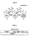
- Fig. 1 shows a network for data transport in conformity with the IEEE 1394 standard.
- the IEEE 1394 defines physical layer, link layer, transaction layer, and serial bus management.
- an application layer is usually implemented as an upper layer.
- those layers that do not directly relate to the present invention are omitted for the sake of simplicity.
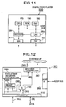
- an IEEE1394 network is composed of a plurality of nodes each having physical layer (PHY) device, which are connected in cascade through predetermined cables.
- the port of PHY device 10 is connected to a port of PHY device 11 by a cable 60 and the other port of the PHY device 11 is connected to a port of PHY device 12 by a cable 61.
- An IEEE1394 PHY device has a repeater function of inputting data on one port and outputting the data on all other ports thereof. Accordingly, the network of Fig. 1 is physically formed in tree topology but logically in bus topology.
- a PHY device is referred to as a PHY LSI (large scale integration) because a PHY device is usually available as an LSI.
- a PHY LSI operates according to a clock signal generated by an external crystal oscillator.
- the respective PHY LSIs 10-12 have crystal oscillators 30-31 attached thereto.
- the resonance frequency f r of a crystal oscillator is 24.576MHz with a permissible deviation of ⁇ 100ppm (parts per million).
- the IEEE1394 standard defines transport rates: S100, S200, and S400, which correspond to 4 ⁇ f r (98.304 Mbits per second), 8 ⁇ f r (196.608 Mbits per second), and 16 ⁇ f r (393.216 Mbits per second), respectively. Since a clock signal at each node is in free-running state without frequency synchronization control, the PHY LSIs 10-12 may be operating in accordance with different clock frequencies within the permissible deviation of ⁇ 100ppm.
- an isochronous cycle mode has been introduced in the IEEE1394 standard.
- the isochronous cycle mode only a node that has obtained a necessary bandwidth and gotten the right to transmit can transmit an isochronous stream packet. Since the isochronous cycle occurs in a period of 125 ⁇ sec, it ensures real-time transport of a stream of data.
- the isochronous cycle starts after transmission of a cycle start packet, which is transmitted by a node functioning as a cycle master.
- a cycle start packet which is transmitted by a node functioning as a cycle master.
- the cycle start packet includes time information at which the packet itself was transmitted.
- a cycle time register provides this time information.
- the cycle master 50 writes a value of its own cycle time regisLer 40 on a cycle start packet when transmitting it to the IEEE1394 bus.
- a cycle time register has a length of 32 bits, which is divided into 7-bit second count field, 13-bit cycle count field, and 12-bit cycle offset field.
- the cycle offset field is a counter which counts according to a physical layer clock of 24.576MHz such that a counter value is incremented by one from 0 to 3071 before resetting to zero and starting again. Accordingly, the counter value is reset to zero at intervals of 125 ⁇ sec.
- the cycle count field is a counter which counts at intervals of 125 ⁇ sec. Its counter value is incremented by one when the cycle offset field is reset to zero, from 0 to 7999 before resetting to zero and starting again, and therefore it is reset to zero at intervals of 1 second.
- the second count field is a counter which counts at intervals of 1 second. Its counter value is incremented by one when the cycle count field is reset to zero, from 0 to 127 before resetting to zero and starting again.
- a cycle time register (40, 41, 42) is implemented in a space of a control and status register (CSR) provided in the serial bus management (not shown).
- CSR control and status register
- a link layer LSI (20, 21, 22) is separated from a corresponding cycle time register (40, 41, 42).
- the cycle time register is usually also implemented in the link layer LSI.
- the link layer LSI (20, 21, 22) operates according to a clock frequency of 49.152 MHz, which is twice the physical layer clock frequency of 24.576MHz. In the link layer LSI, the clock frequency of 49.152 MHz is divided by 2 to produce the physical layer clock frequency of 24.576MHz, which causes the cycle time register to operate.
- Any node other than the cycle master receives the cycle start packet including the time information from the cycle master and overwrites a clock cycle offset value of its own cycle time register with the received time information to synchronize to the cycle master. In this manner, the contents of the cycle time register of each node are adjusted ever time the cycle start packet is received at intervals of 125 ⁇ sec so as to establish time information synchronization of all nodes.
- the time information synchronization is performed among the nodes 50-52.
- the PHY clock frequency of the crystal oscillator 31 in the node 51 is higher than that of the crystal oscillator 30 in the node 50 (cycle master) and the PHY clock frequency of the crystal oscillator 32 in the node 52 is lower than that of the crystal oscillator 30.
- the cycle start packet is transmitted when the cycle offset value of the cycle time register 40 is reset from 3071 to zero at the rising edge of the PHY clock and the time information written in the cycle start packet is a cycle offset value of zero, that the other nodes 51 and 52 receive the cycle start packet from the cycle master 50 without delay, and that the overwriting of the cycle offset at the nodes 51 and 52 is performed at the rising edge of the PHY clock.
- the cycle offset value is continuously reset to zero twice, which means a delay of one clock, resulting in time adjustment with a maximum adjusted amount of one clock. Since one clock is about 40 nanosecond, frequency fluctuations (variations in cycle time register value) of up to about 320 ppm will occur with respect to a period of 125 ⁇ sec.
- the contents of the cycle time register is used for real-time transport of audiovisual stream (AV stream) defined by IEC 61883 standard.
- AV stream audiovisual stream
- To receive the AV stream it is necessary for a receiving side to decode it by. faithfully reproducing the video frame frequency and audio sampling frequency that were used at the transmitting side.
- these media-dependent frequencies do not synchronize with frequencies used in the IEEE1394 standard.
- the transmitting side transmits a packet of data attaching frequency information as a time stamp and the receiving side, when receiving the packet, looks at this time stamp to reproduce the frequency information.
- the IEC61883 standard defines that such time stamp information is determined depending on the cycle time register of the transmitting side.
- a bridge has a plurality of portals, each of which is connected to a corresponding IEEE1394 bus.
- the bridge 70 has portals 80a and 80B each connected to IEEE1394 buses 90 and 91.
- the IEEE1394 buses 90-92 have cycle masters 100-102 predetermined according to IEEE1394 standard.
- a portal may function as a cycle master because it also functions as an IEEE node.
- One of the cycle masters 100-102 is selected as a net cycle master that is a cycle master for the entire bridge network.
- the cycle master 102 is designated as a net cycle master for the bridge network.
- the other cycle masters 100 and 101 synchronize their own time information to the time information of the net cycle master 102 using the following procedure.
- the portal 81B of the bridge 71 synchronizes its own time information to the net cycle master 102 using a cycle start packet received from the net cycle master 102.
- the other portal 81A of the bridge 71 synchronizes its own time information to the cycle master 101 using a cycle start packet received from the cycle master 101. Accordingly, the bridge 71 can detect a time deviation of the cycle master 101 from the net cycle master 102 by comparing the time information of the cycle master 101 to that of the net cycle master 102. When such a time deviation has been detected, the portal 81A transmits a control packet to the cycle master 101 to adjust the cycle time register of the cycle master 101.
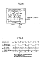
- a control packet which is also called a cycle master adjustment packet, is formed according to a special isochronous stream packet format having no data field. Because of no data field, the value of a data length field is zero.
- a combination of tag and channel fields designates this packet as a control packet for cycle time adjustment.
- the tag and channel fields store "3" and "31", respectively.
- a transaction code (tcode) field stores "10" to indicate that this packet is based on the isochronous stream packet format.
- a synchronization code (sy) field stores a value designating an amount to be adjusted in the cycle time register of a cycle master receiving this packet. For example, when the synchronization code (sy) field stores a value of 1, a cycle master that has received the control packet elongates a period of the following isochronous cycle (125 ⁇ sec) by one cycle offset of about 40 nanoseconds. On the other hand, when the synchronization code (sy) field stores a value of 3, a cycle master that has received the control packet shortens a period of the following isochronous cycle (125 ⁇ sec) by one cycle offset of about 40 nanoseconds.
- the cycle master 101 can operate the bus 91 with the isochronous cycle synchronizing to that of the bus 92 connected to the net cycle master 102. Therefore, the bus 91 synchronizes to the bus 92. Since the synchronization control for the bridge network is designed to synchronize the isochronous cycle periods, the values of second count field and cycle count field of a bus do not always coincide with those of another bus (see Fig. 2).
- the bridge 70 performs the same synchronization control as the bridge 71.
- the bus 90 synchronizes to the bus 91 that synchronizes the bus 92. Therefore, all the buses 90-92 synchronize.
- Such a synchronization method is disclosed in Japanese Patent Application Unexamined Publication Nos. P2000-307557A and P2000-32030A.
- the synchronization control in the bridge network is performed by appropriately elongating or shortening a period of isochronous cycle (125 ⁇ sec) by one cycle offset of about 40 nanoseconds, resulting in an instantaneous frequency fluctuation of approximately 320 ppm when adjusted.
- the synchronization control in the bridge network is performed by sequentially establishing synchronization from a bus to the adjacent bus to synchronize all the buses.
- frequency fluctuations due to the above synchronization control of isochronous cycle within an IEEE1394 bus or a bridge network composed of a plurality of IEEE1394 buses adversely influence the quality of transmission of a received real-time stream.
- frequency fluctuations may be accumulated every time the synchronization control is performed for one bridge, resulting in a large amount of frequency deviation. It is the same with other communication networks having a function of notifying time information at regular intervals.
- An object of the present invention is to provide a network synchronization method and system allowing reliable transmission system by reducing frequency fluctuations of isochronous cycle due to the synchronization control.
- a method for synchronizing a plurality of devices connected to a network wherein the devices have time information individually varying in a predetermined time period of T, wherein a time master device that is one of the devices periodically notifies its own time information as master time information to time slave devices that are devices other than the time master device
- said method includes the steps of: at each of the time slave devices, preparing update-possible time points having a period of T/N (N is an integer greater than 1); receiving the master time information from the time master device; and updating its own time information using the master time information at an update-possible time point just after the master time information has been received.
- a network device connected to a network includes: a clock generator for generating a clock signal; a physical-layer circuit connected to the clock generator; and a link-layer circuit connected to the physical-layer circuit, wherein the link-layer circuit comprises: a timing generator for generating a first timing signal and a second timing signal from a system clock signal inputted from the physical-layer circuit, wherein the first timing signal is generated in a period of T and the second timing signal is generated at a time point corresponding to a period of T/N (N is an integer greater than 1); a time information memory for storing Lime information, which varies according to the first timing signal; and a controller controlling the time information memory such that, when receiving reference time information from the network, the time information stored in the time information memory is updated using the reference time information at a time point according to the second timing signal just after the reference time information has been received.
- the timing generator may include: a frequency divider for dividing the system clock signal in frequency by two to produce the first timing signal having the period of T; and a frequency multiplier for multiplying the system clock signal in frequency by two to produce the second timing signal having a period of T/2.
- the timing generator may include: a frequency multiplier for multiplying the system clock signal in frequency by two to produce a timing signal having a period of T/2; and a base-4 counter for counting from 0 to 3 according to the timing signal to produce the first timing signal every time the base-4 counter is reset to 0, wherein, when the reference time information has been received, the base-4 counter is reset to 0 to generate the second timing signal.
- the timing generator may include: a binary counter for counting according to the system clock signal to produce the first timing signal every time the binary counter is reset to 0, wherein, when the reference time information has been received, the binary counter is reset to 0 to generate the second timing signal.
- a bridge connecting a plurality of networks, each of which individually has time information varying in a predetermined time period of T includes: a first portal connected to a first network having first time information; a second portal connected to a second network having second time information; a time difference detector for detecting a time difference of the second time information with respect to the first time information; an adjustment value generator for producing a time adjustment value based on the time difference, wherein the time adjustment value is an integral multiple of T/M (M is an integer greater than 1); and a controller adjusting the second time information for the second network by the time adjustment value.
- the adjustment value generator may include: a table containing a predetermined correspondence between time differences and time adjustment values, wherein the time adjustment values have a predetermined step of adjustment and an absolute value of a time adjustment value is restricted within a predetermined range, wherein the adjustment value generator produces a time adjustment value corresponding to the time difference by referring to the table.
- a maximum absolute value of the time adjustment values may be a minimum value of integral multiples of the predetermined step of adjustment sufficient for adjusting a largest one of frequency deviations in local clocks of the network.
- the time adjustment value may be set to a predetermined value beyond the predetermined range.
- a method for synchronizing a bridge network composed of at least one bridge having a plurality of portals each connected to different networks, each of which includes at least one node, wherein each of the portals and networks individually has a clock generator by which time information varies in a predetermined time period of T, wherein one of the portals is a master portal and the others are slave portals
- said method includes the steps of: a) detecting a time difference of slave time information of each slave portal with respect to master time information of the master portal; b) producing a time adjustment value based on the time difference, wherein the time adjustment value is an integral multiple of T/M (M is an integer greater than 1); and c) adjusting the slave time information by the time adjustment value.
- a method for synchronizing a bridge network composed of at least one bridge having a plurality of portals each connected to different networks, each of which includes at least one node, wherein each of the portals and networks individually has a clock generator by which time information varies in a predetermined time period of T, wherein one of the portals is a master portal and the others are slave portals
- said method includes the steps of: a) each of portals detecting a lowest clock accuracy in a corresponding network; b) dynamically determining a maximum adjustment value based on a network-wide lowest clock accuracy selected from lowest clock accuracies detected by the portals; c) detecting a time difference of slave time information of each slave portal with respect to master time information of the master portal; d) producing a time adjustment value within the dynamically determined maximum adjustment value based on the time difference, wherein the time adjustment value is an integral multiple of T/M (M is an integer greater than 1); and e) adjusting the slave time information by
- a 1394 link-layer LSI 20A is employed in a node of, for example, the IEEE1394 network as shown in Fig. 1.
- the 1394 link-layer LSI 20A is provided with a physical-layer/link-layer (PHY/LINK) interface 110 through which plural signals (e.g. in the neighborhood of nine kinds of signals) are inputted and outputted from and to the PHY LSI.
- PHY/LINK physical-layer/link-layer
- SCLK system clock signal
- SCLK system clock signal
- the PHY/LINK interface 110 is a bidirectional interface to the PHY LSI to exchange packets.
- the 1394 link-layer LSI 20A operates according to the system clock signal SCLK, which has a frequency fs of 49.152 MHz, that is, two times the clock frequency of the crystal oscillator provided in the PHY LSI (see Fig. 1).
- the bit rate per data signal line is 49.152 Mbps.
- S100, S200 and S400 data are transferred using two signal lines, four signal lines, and eight signal lines, respectively.
- the cycle start packet is transferred in S100 and therefore two signal lines are used to receive it from the PHY LSI.
- the system clock signal SCLK is output to a frequency divider 120, a frequency multiplier 130, and a packet receiver 140.
- the frequency divider 120 divides the frequency fs of the system clock signal SCLK by two to produce a fs/2 clock of 24.576 MHz, which is supplied to a cycle time register controller 150.
- the frequency multiplier 130 multiplies the frequency fs of the system clock signal SCLK by two to produce a 2fs clock of 98.304 MHz, which is supplied to the cycle time register controller 150.
- the PHY/LINK interface 110 converts a received packet of data into a 32-bit parallel signal and outputs it to the packet receiver 140.
- the packet receiver 140 performs bit-error check and packet type check of the input packet according to the system clock signal SCLK and distributes it to destinations depending on the packet type.
- SCLK system clock signal
- the cycle time register controller 150 is depicted as one destination.
- the packet receiver 140 When receiving the cycle start packet, the packet receiver 140 outputs time information included in the received cycle start packet to the cycle time register controller 150.
- the cycle time register controller 150 is a functional block that controls the value of the cycle time register depending on the time information inputted from the packet receiver 140 and the 1/2fs clock and the 2fs clock from respective ones of the frequency divider 120 and the frequency multiplier 130.
- the internal circuit of the 1394 link-layer LSI 20A is integrated in a circuit block.
- Fig. 6 only blocks related to the present invention are depicted for the sake of simplicity.
- the cycle time register controller 150 increments the cycle offset value of the cycle time register at the rising edge of the 1/2fs clock and overwrites the cycle offset value with the input time information at timing of the rising edge of the 2fs clock. For example, when a cycle start packet having a cycle offset value of "34" as time information is received at the timing as indicated by an arrow, the overwriting of the cycle offset value with "34" is performed at the rising edge of the 2fs clock immediately after the receipt of the cycle start packet. At the rising edge of the 1/2fs clock immediately after that, the cycle offset value is incremented to "35".
- the cycle time register can be adjusted with a resolution of about 10 nanoseconds. This allows much accurate time adjustment to the cycle master, compared to the conventional one-cycle offset adjustment (in steps of about 40 nanoseconds). Accordingly, the isochronous cycle period of about 125 ⁇ sec can be adjusted more precisely, resulting in reduced frequency fluctuations at each node.
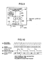
- step S101 it is determined whether a cycle start packet is received (step S101).
- step S102 When no cycle start packet is received (NO in step S101), it is determined whether the present timing is coincident to the rising edge of the 1/2fs clock (step S102).
- step S103 At the rising edge of the 1/2fs clock (YES in step S102), it is further determined whether the cycle offset value is equal to "3071" (step S103).
- step S104 the cycle offset value is incremented by one (step S104) and the control goes back to the step S101.
- step S105 the cycle count value of the cycle time register is incremented by one and resets the cycle offset value to zero (step S105). Thereafter, the control goes back to the step S101.
- step S101 When a cycle start packet is received (YES in step S101), it is determined whether the present timing is coincident to the rising edge of the 2fs clock (step S106). At the rising edge of the 2fs clock (YES in step S106), the existing cycle offset value is overwritten with the time information included in the received cycle start packet (step S107). Thereafter, the control goes back to the step S101.
- a link-layer LSI 20B according to a modified example of the first embodiment is provided with a base-4 counter 160 instead of the frequency divider 120.
- the other circuit blocks are the same as those in the link-layer LSI 20A of Fig. 6. Accordingly, these blocks are denoted by the same reference numerals and the details will be omitted.
- the base-4 counter 160 increments by one from 0 to 3 before resetting to zero and starting again and is forced to be reset to zero when the packet receiver 140 outputs time information included in a received cycle start packet.
- the base-4 counter 160 when reset to zero, outputs a pulse signal to the cycle time register controller 150.
- the base-4 counter 160 increments by one from 0 to 3 according to the 2fs clock received from the frequency multiplier 130 and outputs the pulse signal to the cycle time register controller 150 when it is reset to zero (see Fig. 10(g)).
- the cycle time register controller 150 increments the cycle offset value of the cycle time register when the pulse signal is received from the base-4 counter 160.
- the base-4 counter 160 When a cycle start packet is received and its time information is output to the cycle time register controller 150, the base-4 counter 160 is forced to be reset to zero, which causes the pulse signal to be output to the cycle time register controller 150.
- the cycle time register controller 150 overwrites the cycle offset value with the time information received from the packet receiver 140.
- the base-4 counter 160 is forced to be reset to zero, which causes the pulse signal to be output to the cycle time register controller 150. Accordingly, the overwriting of the cycle offset value with "34" is performed at the rising edge of the 2fs clock immediately after the receipt of the cycle start packet. At the rising edge of a pulse signal immediately after that, the cycle offset value is increased to "35".
- the base-4 counter 160 is forced to be reset to zero. Therefore, the overwritten cycle offset value is surely held for a lapse of one cycle offset period after the overwriting.
- This modified example employing the base-4 counter 160 uses only one clock (2fs clock), resulting in further stable operation at each node.
- frequency fluctuations can be effectively reduced.
- the cycle time register can be adjusted with a resolution of about 10 nanoseconds. This allows much accurate time adjustment to the cycle master, compared to the conventional one-cycle offset adjustment (in steps of about 40 nanoseconds). Accordingly, the isochronous cycle period of about 125 ⁇ sec can be adjusted more precisely, resulting in reduced frequency fluctuations at each node.
- an n-fold frequency multiplier (n - 4, 8, or other number) may be used to obtain a higher resolution.
- a digital video player 220 employs a link-layer LSI 20C according to a second embodiment of the present invention.
- the digital video player 220 further includes a PHY LSI 10, a processor (CPU) 170, a ROM 180, RAM 190, a decoder 200, and a digital-to-analog converter 210.
- the digital video player 220 decodes a digital video signal of DV format received from the IEEE1394 bus and outputs an analog video signal.
- the digital video signal of DV format is mapped into isochronous stream packet following IEC 61883 standard. More specifically, the upper eight bytes of the data field of an isochronous stream packets are defined as a header of a common isochronous packet (CIP) in the IEC 61883 standard. The type of video format and time stamp information are stored in the CIP header.
- CIP common isochronous packet
- the link-layer LSI 20C has a host interface to a host bus connected to other components including the processor (CPU) 170 and a stream interface to the decoder 200 for input and output of isochronous stream packets which are needed to be processed at high speeds.
- the processor 170 performs software processing of IEEE1394 protocols of transaction layer and the like.
- the decoder 200 also has a host interface and a stream interface similar to those of the link-layer LSI 20C.
- the link-layer LSI 20C is provided with a physical-layer/link-layer (PHY/LINK) interface 110 through which plural signals (e.g. in the neighborhood of nine kinds of signals) are inputted and outputted from and to the PHY LSI 10.
- PHY/LINK physical-layer/link-layer
- SCLK system clock signal
- the PHY/LINK interface 110 is a bidirectional interface to the PHY LSI 10 to exchange packets.
- the 1394 link-layer LSI 20C operates according to the system clock signal SCLK, which has a frequency fs of 49.152 MHz, that is, two times the clock frequency of the crystal oscillator provided in the PHY LSI 10.
- SCLK system clock signal
- a packet inputted from the IEEE1394 bus enters a packet receiver 140 through the PHY/LINK interface 110.
- the packet receiver 140 determines that the input packet is an isochronous stream packet, the packet of data is output to an IEC61883 termination 240.
- the packet receiver 140 outputs time information included in the cycle start packet to a cycle time register controller 150.
- the IEC61883 termination 240 reconstructs DV data based on information stored in the CIP header and produces a nominal video frame pulse of approximate 30 Hz from the time stamp stored in the CIP header and time information inputted from the cycle time register of its own and outputs them to the stream interface.
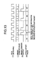
- the 1394 link-layer LSI 20C performs cycle time register control using a binary counter 230 that operates according to the system clock signal SCLK.
- the binary counter 230 alternately indicates '0' and '1' and is forced to be reset to zero when a cycle start packet is received.
- the binary counter 230 outputs a pulse signal when the binary counter 230 indicates zero.
- the cycle time register controller 150 performs the cycle time register control using the output of the binary counter 230, the system clock signal SCLK, and a received cycle start packet, which will be described with reference to Fig. 13.
- the binary counter 230 outputs the pulse signal to the cycle time register controller 150 when it is reset to zero (see Fig. 13(k)).
- the cycle time register controller 150 increments the cycle offset value of the cycle time register when the pulse signal is received from the binary counter 230.
- the binary counter 230 When a cycle start packet is received and its time information is output to the cycle time register controller 150, the binary counter 230 is forced to be reset to zero, which causes the pulse signal to be output to the cycle time register controller 150. When the pulse signal is received, the cycle time register controller 150 overwrites the cycle offset value with the time information received from the packet receiver 140.
- the binary counter 230 is forced to be reset to zero, which causes the pulse signal to be output to the cycle time register controller 150. Accordingly, the overwriting of the cycle offset value with "35” is performed at the rising edge of the system clock signal SCLK immediately after the receipt of the cycle start packet. At the rising edge of a pulse signal immediately after that, the cycle offset value is increased to "36".
- the binary counter 230 is forced to be reset to zero. Therefore, the overwritten cycle offset value is held for a lapse of one cycle offset period after the overwriting.
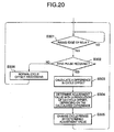
- step S201 it is determined whether the system clock signal SCLK goes high (step S201) and, at the rising edge of the system clock signal SCLK (YES in step S201), it is further determined whether a cycle start packet has been received (step S202). When no cycle start packet is received (NO in step S202), it is determined whether the binary counter 230 is equal to 0 (step S203).
- step S203 When Lhe binary counter 230 is not equal to 0, that is, 1 (NO in step S203), the binary counter 230 is reset to 0 (step S204) and the control goes back to the step S201.
- step S204 When the binary counter 230 is equal to 0 (YES in step S203), it is further determined whether the cycle offset value is equal to "3071" (step S205).
- step S206 When it is not equal to "3071” (NO in step S205), the cycle offset value is incremented by one (step S206). When it is equal to "3071” (YES in step S205), the cycle count value of the cycle time register is incremented by one and resets the cycle offset value to zero (step S208). After the step S206 or S208, the binary counter 230 is set to 1 (step S207) and the control goes back to the step S201.
- step S202 When a cycle start packet is received (YES in step S202), the binary counter 230 is reset to 0 (step S209) and the existing cycle offset value is overwritten with the time information included in the received cycle start packet (step S210). Thereafter, the control goes back to the step S201.
- the isochronous cycle period of about 125 ⁇ sec can be adjusted more precisely, resulting in reduced frequency fluctuations, which achieves reduced jitter of the frame pulse signal. Therefore, the digital video player 220 can decode a high-quality video signal.
- the second embodiment as shown in Fig. 12 employs no frequency multiplier, resulting in more simplified circuit structure.
- the cycle time register control is performed by the cycle time register controller 150 provided in the link-layer LSI 20C.
- the cycle time register control program may be previously stored in the ROM 180.
- a bridge 70A connects two IEEE1394 buses 90 and 91 and the bridge 70A is composed of portals 80A and 80B, which are connected to the buses 90 and 91, respectively.
- the respective buses 90 and 91 are connected to nodes 50 and 51.
- the node 50 functions as a cycle master of the bus 90 and a net cycle master for the entire bridge network.
- the portal 80B of the bridge 70A functions as a cycle master of the bus 91. Therefore, the bridge 70A performs synchronization of the portal 80B to the portal 80A.
- the portal 80A is a master portal and the portal 80B is a slave portal.
- the slave portal 80B as the cycle master of the bus 91 notifies the bus 91 by a cycle start packet of time information obtained by the cycle time register control, so that synchronization is established in the entire bridge network.
- the bridge 70A includes an inter-bus synchronization control circuit composed of the master portal 80A and the slave portal 80B.
- the master portal 80A includes a cycle time register controller 150A.
- the slave portal 80b includes a frequency multiplier 130, a cycle time register controller 150B, an error detector 260, and an adjustment value generator 270.
- the cycle time register controller 150A synchronizes to the net cycle master 50 according to an appropriate synchronization control as described before. Every time a cycle offset value (cycle_offset) of the cycle time register incorporated in the master portal 80A is coincident to a predetermined value, the cycle time register controller 150A outputs a sync pulse to the error detector 260 of the slave portal 80B.
- the error detector 260 operates according to a 2fs clock signal of 98.304 MHz, which is generated by the frequency multiplier 130.
- the frequency multiplier 130 multiplies the frequency fs of the system clock signal SCLK by two to produce the 2fs clock of 98.304 MHz, which is supplied to the error detector 260 and a cycle time register controller 150B.
- the error detector 260 has a base-4 counter incorporated therein. By using the base-4 counter, the error detector 260 can detect an error from the net cycle master with a resolution of about 10 nanoseconds, which is one-fourth of one cycle offset of about 40 nanoseconds.
- the error detector 260 When having received the sync pulse from the cycle time register controller 150A, the error detector 260 inputs a cycle offset value of the cycle time register incorporated in the cycle time register controller 150B. Then, the predetermined value (here, 3070) is subtracted from the cycle offset value of the slave portal 80B to produce a cycle offset error of the slave portal 80b with respect to the master portal 80A. A detected error cycle is obtained by adding the cycle offset error to one-fourth of a value of the base-4 counter at that time point. An example of time adjustment will be described with reference to Figs. 17A and 17B.
- cycle_offset a cycle offset value of the cycle time register incorporated in the master portal 80A
- cycle_offset a cycle offset value of the cycle time register incorporated in the master portal 80A
- a cycle offset error is -1, which is obtained by subtracting 3070 from 3069. Since the base-4 counter indicates "2", a detected error cycle is -1/2, which is obtained by adding 2/4 to -1. This means that the cycle offset of the slave portal 80B lags that of the master portal 80A by 1/2 cycle.
- the adjustment value generator 270 generates a cycle period time adjustment value in the slave portal 80B based on the detected error cycle inputted from the error detector 260, which will be described in detail later.
- the cycle time register controller 150B inputs the cycle period time adjustment value from the adjustment value generator 270 and increases or decreases a cycle period of 125 ⁇ sec by the cycle period time adjustment value. This cycle period time adjustment value is also determined with a resolution of one-fourth of one cycle offset. Since the portal 80B is a cycle master for the bus 91, the portal 80B transmits a cycle start packet depending on the adjusted timing, so that the buses 90 and 91 are synchronized.
- adjustment value generator 270 a relationship between input cycle errors and output adjustment values is determined as described hereinafter.
- the adjustment value may be set to 0 regardless of absolute values of error.
- the adjustment value may be set based on a history of adjustment values or so-called integral control.
- an adjustment value much larger than the clock frequency accuracy may be used to rapidly establish synchronization. For example, when the absolute value of error is greater than 100-cycle offset, the adjustment value is set to 32-cycle offset.
- another node may be a cycle master of the bus 91.
- a node 51 may be the cycle master.
- the functions defined in P1394.1 standard as described before is needed in the portal 80B and the node 51.
- the adjustment value of P1394.1 standard is fixed to ⁇ 1-cycle offset. Accordingly, the synchronization code (sy) field is necessarily defined so as to allow a higher resolution of adjustment.
- a bridge network employing a bridge according to a fourth embodiment of the present invention is similar to that of the third embodiment as shown in Fig. 15.
- a bridge 70A connects two IEEE1394 buses 90 and 91 and the bridge 70A is composed of portals 80A and 80B, which are connected to the buses 90 and 91, respectively.
- the respective buses 90 and 91 are connected to nodes 50 and 51.
- the node 50 functions as a cycle master of the bus 90 and a net cycle master for the entire bridge network.
- the portal 80B of the bridge 70A functions as a cycle master of the bus 91. Therefore, the bridge 70A performs synchronization of the portal 80B to the portal 80A.
- the portal 80A is a master portal and the portal 80B is a slave portal.
- the slave portal 80B as the cycle master of the bus 91 notifies the bus 91 by a cycle start packet of time information obtained by the cycle time register control, so that synchronization is established in the entire bridge network.
- the bridge 70A includes an inter-bus synchronization control circuit composed of the master portal 80A and the slave portal 80B.
- the master portal 80A includes a cycle time register controller 150A and a binary counter 230.
- the slave portal 80b includes a cycle time register controller 150B, an error detector 260, and an adjustment value generator 270.
- the cycle time register controller 150A synchronizes to the net cycle master 50 by receiving a cycle start packet from the net cycle master with a resolution of the system clock system SCLK, which is employed in the second embodiment (see Figs. 12 and 13). More specifically, the binary counter 230 operates according to the system clock signal SCLK and outputs a pulse to the cycle time register controller 150A every time its count is equal to 0. Further, the binary counter 230 is reset to zero when the cycle start packet has been received. The cycle offset value of the cycle time register incorporated in the cycle time register controller 150A is incremented by one according to the output of the binary counter 230.
- cycle_offset Every time the cycle offset value (cycle_offset) of the cycle time register is coincident to a predetermined value (here, 3070), the cycle time register controller 150A outputs a sync pulse to the error detector 260 of the slave portal 80B. In this manner, the synchronization control of the cycle time register is performed with a resolution of the system clock signal SCLK, resulting in reduced frequency deviations of the cycle time register.
- the system clock signal SCLK is supplied to the error detector 260 and a cycle time register controller 150.
- the error detector 260 operates according to the system clock signal SCLK.
- the error detector 260 inputs a cycle offset value of the cycle time register incorporated in the cycle time register controller 150B.
- the predetermined value here, 3070
- cycle_offset a cycle offset value of the cycle time register incorporated in the master portal 80A
- cycle_offset a cycle offset value of the cycle time register incorporated in the master portal 80A
- a cycle offset error is +1, which is obtained by subtracting 3070 from 3071. This means that the cycle offset of the slave portal 80B leads that of the master portal 80A by one cycle.
- the adjustment value generator 270 generates a cycle period time adjustment value in the slave portal 80B based on the detected error cycle and a predetermined correspondence table.
- the one-cycle offset is used as the maximum adjustment value and the relationship between errors and adjustment values is shown, as an example, in TABLE II.
- the adjustment value generator 270 when the cycle offset error is +1, the adjustment value generator 270 generates a cycle period time adjustment value of +1/2-cycle offset.
- the cycle time register controller 150B inputs the cycle period time adjustment value of +1/2-cycle offset and increases a cycle period of 125 ⁇ sec by 1/2-cycle offset as shown in Fig. 19B. Since the portal 80B is a cycle master for the bus 91, the portal 808 transmits a cycle start packet depending on the adjusted timing, so that the buses 90 and 91 are synchronized.
- step S301 it is determined whether the system clock signal SCLK goes high (step S301) and, at the rising edge of the system clock signal SCLK (YES in step S301), it is further determined whether a sync pulse has been received (step S302). When no sync pulse is received (NO in step S302), normal cycle offset processing is performed (step S306) and the control goes back to the step S301.
- the error detector 260 subtracts the predetermined value (here, 3070) from the cycle offset value of the slave portal 80B to produce a difference in cycle offset of the slave portal 80B with respect to the master portal 80A (step S303).
- the adjustment value generator 270 generates a cycle period time adjustment value in the slave portal 80B based on the calculated difference and the correspondence table (TABLE II) and the cycle time register controller 150B changes the cycle period by the cycle period time adjustment value (step S305).
- a bridge 70B according to a fifth embodiment of the present invention has three or more portals, each of which is connected to a corresponding IEEE1394 bus.
- the bridge 70B is provided with four portals 80A-80D each having buses 90-93 connected thereto, and it is assumed that each portal is a cycle master for a corresponding bus and the portal 80A functions as the net cycle master.
- the bridge 70B is functionally divided into the master portal 80A and other slave portals 80B-80D. Every time a cycle offset value (cycle_offset) of the cycle time register incorporated in the master portal 80A is coincident to "3070", the cycle time register controller 150A outputs a sync pulse to the slave portals 80B-80D.
- the slave portals 80B-80D individually perform synchronization control based on the sync pulse received from the master portal 80A.
- the synchronization control in each slave portal is basically the same as that in the fourth embodiment (see Fig .18) but it is different from the fourth embodiment in a function of dynamically determining the maximum adjustment value. Details of this function will be described below.
- the maximum adjustment value can be dynamically determined depending on the clock frequency accuracy of devices actually connected to the network.
- the bridge 70B implements such a function of dynamically determining the maximum adjustment value.
- the master portal 80A is provided with a clock frequency accuracy investigator 280A and a maximum adjustment value decision section 290.
- the respective slave portals 80B-80D are provided with clock frequency accuracy investigators 280B-280D.
- Each of the clock frequency accuracy investigators 280A-280D investigates the clock frequency accuracy of a node connected to a corresponding bus. More specifically, the clock frequency accuracy information has been written in the cyc_clk_acc field of a configuration ROM area where node performance information has been stored. It is enough to read the clock frequency accuracy information from a portal and a cycle master within a corresponding bus. When there is a possibility that its cycle master changes depending on insertion or removal of a node, it is necessary to update the investigation result as occasion demands.
- the cyc_clk_acc values of all nodes may be investigated regardless of node type such as portal or cycle master.
- the cyc_clk_acc field implementation is not necessary. Therefore, even if a read request is sent to all nodes, a node having no cyc_clk_acc field implemented cannot respond to the read request. In reality, almost all nodes having the cycle master function are expected to have the cyc_clk_acc field implemented. Accordingly, this cyc_clk_acc value reading procedure can be effectively used.
- the clock frequency accuracy investigator of a corresponding slave portal detects the lowest one of the read clock frequency accuracies and outputs it to the maximum adjustment value decision section 290 of the master portal 80A.
- the maximum adjustment value decision section 290 detects the network-wide lowest one of the lowest clock frequency accuracies received from the slave portals 80B-80D and determines the maximum adjustment value based on the network-wide lowest clock frequency accuracy.
- the maximum adjustment value decision section 290 outputs it to the adjustment value generators 270B-270D of the slave portals 80b-80D. Using the maximum adjustment value, each of the slave portals 80b-80D performs the synchronization control as described before.
- each portal investigates the clock frequency accuracy of a node connected to the corresponding bus.
- one or more predetermined node may investigate the clock frequency accuracy of a node connected to another bus that is not connected to the predetermined node.
- the investigation result of clock frequency accuracy for each bus is reported to the master portal 80A and the maximum adjustment value obtained from the investigation result is notified to all slave portals 80B-80D.
- This dynamically adjustment value determination operation is completely performed within the bridge 70B. However, it can be performed over a plurality of bridges by an additional protocol such as a new message format to exchange information between IEEE1394 buses.
- the present invention is not restricted to the case of IEEE1394 standard. As long as time information is notified at regular intervals to synchronize a plurality of network devices, the present invention can be applied to such a system.
- frequency fluctuations caused by time information synchronization in a network can be reduced, resulting in improved quality of transmission of real-time data such as audiovisual stream through the network.
Priority Applications (1)
| Application Number | Priority Date | Filing Date | Title |
|---|---|---|---|
| EP06016712A EP1729200A1 (fr) | 2001-06-15 | 2002-06-14 | Téchnique de synchronisation de réseau |
Applications Claiming Priority (2)
| Application Number | Priority Date | Filing Date | Title |
|---|---|---|---|
| JP2001181220 | 2001-06-15 | ||
| JP2001181220A JP3698074B2 (ja) | 2001-06-15 | 2001-06-15 | ネットワーク同期方法、lsi、バスブリッジ、ネットワーク機器、およびプログラム |
Related Child Applications (1)
| Application Number | Title | Priority Date | Filing Date |
|---|---|---|---|
| EP06016712A Division EP1729200A1 (fr) | 2001-06-15 | 2002-06-14 | Téchnique de synchronisation de réseau |
Publications (2)
| Publication Number | Publication Date |
|---|---|
| EP1267506A2 true EP1267506A2 (fr) | 2002-12-18 |
| EP1267506A3 EP1267506A3 (fr) | 2006-02-15 |
Family
ID=19021525
Family Applications (2)
| Application Number | Title | Priority Date | Filing Date |
|---|---|---|---|
| EP02013182A Withdrawn EP1267506A3 (fr) | 2001-06-15 | 2002-06-14 | Téchnique de synchronisation de réseau |
| EP06016712A Withdrawn EP1729200A1 (fr) | 2001-06-15 | 2002-06-14 | Téchnique de synchronisation de réseau |
Family Applications After (1)
| Application Number | Title | Priority Date | Filing Date |
|---|---|---|---|
| EP06016712A Withdrawn EP1729200A1 (fr) | 2001-06-15 | 2002-06-14 | Téchnique de synchronisation de réseau |
Country Status (4)
| Country | Link |
|---|---|
| US (2) | US7055050B2 (fr) |
| EP (2) | EP1267506A3 (fr) |
| JP (1) | JP3698074B2 (fr) |
| CN (1) | CN1392707A (fr) |
Cited By (4)
| Publication number | Priority date | Publication date | Assignee | Title |
|---|---|---|---|---|
| FR2937817A1 (fr) * | 2008-10-24 | 2010-04-30 | Univ Claude Bernard Lyon | Procede de synchronisation temporelle, equipements principal et secondaire pour la mise en oeuvre de ce procede, procede de fonctionnement de ces equippements principal et secondaire |
| WO2014090448A1 (fr) * | 2012-12-14 | 2014-06-19 | Continental Automotive Gmbh | Synchronisation de paquets de données dans un système de transmission de données d'un véhicule |
| CN111030909A (zh) * | 2020-03-03 | 2020-04-17 | 南京科远智慧科技集团股份有限公司 | 一种应用于can总线多主设备通讯间时间同步的方法 |
| CN113760811A (zh) * | 2021-08-19 | 2021-12-07 | 武汉华中数控股份有限公司 | 数控系统多种现场总线的混联总线协议架构及其通信方法 |
Families Citing this family (25)
| Publication number | Priority date | Publication date | Assignee | Title |
|---|---|---|---|---|
| US7684413B2 (en) * | 2002-10-09 | 2010-03-23 | Juniper Networks, Inc. | System and method for rate agile adaptive clocking in a packet-based network |
| JP4178552B2 (ja) * | 2003-07-24 | 2008-11-12 | 株式会社安川電機 | マスター・スレーブ同期通信方式 |
| JP4228081B2 (ja) * | 2003-09-19 | 2009-02-25 | トムソン・カノープス株式会社 | データ変換システム |
| CN100370763C (zh) * | 2003-12-29 | 2008-02-20 | 技嘉科技股份有限公司 | 一种主机信息主动更新方法及其系统 |
| DE102004030969A1 (de) * | 2004-06-26 | 2006-01-12 | Robert Bosch Gmbh | Verfahren und Vorrichtung zur Steuerung eines Bussystems sowie entsprechendes Bussystem |
| US7792158B1 (en) * | 2004-08-18 | 2010-09-07 | Atheros Communications, Inc. | Media streaming synchronization |
| JP2008515318A (ja) * | 2004-09-30 | 2008-05-08 | コーニンクレッカ フィリップス エレクトロニクス エヌ ヴィ | 周波数同調可能な装置 |
| US7505450B2 (en) * | 2005-03-23 | 2009-03-17 | Cisco Technology, Inc. | Configuration of failure and acquire timeouts to facilitate recovery from failures in hierarchical mesh networks |
| US20060224766A1 (en) * | 2005-03-31 | 2006-10-05 | Malackowski Donald W | Operating room communication bus and method |
| DE102005061155A1 (de) * | 2005-12-21 | 2007-06-28 | Bosch Rexroth Ag | Kommunikationsstruktur |
| US8180384B1 (en) * | 2006-07-13 | 2012-05-15 | Rf Micro Devices, Inc. | Transmit data timing control |
| US8289542B2 (en) * | 2007-09-12 | 2012-10-16 | Xerox Corporation | Distributed limit-based accounting for print jobs |
| JP4994280B2 (ja) * | 2008-03-26 | 2012-08-08 | ルネサスエレクトロニクス株式会社 | ルート変更型ネットワーク装置及びシステム |
| JP4896057B2 (ja) * | 2008-03-26 | 2012-03-14 | ルネサスエレクトロニクス株式会社 | 送信タイミング変更型ネットワーク装置及びシステム |
| DE102009054961B4 (de) * | 2009-12-18 | 2017-10-12 | Continental Teves Ag & Co. Ohg | Verfahren zur Verringerung der Latenzzeit bei der Datenübertragung innerhalb eines Steuergeräte-Verbundes |
| US9106645B1 (en) * | 2011-01-26 | 2015-08-11 | Symantec Corporation | Automatic reset for time-based credentials on a mobile device |
| EP2527935B1 (fr) * | 2011-05-26 | 2014-12-03 | Siemens Aktiengesellschaft | Procédé destiné au fonctionnement d'un système d'automatisation |
| JP2013083451A (ja) * | 2011-10-06 | 2013-05-09 | Sony Corp | 時刻制御装置、時刻制御方法、およびプログラム |
| US8644350B2 (en) * | 2011-11-23 | 2014-02-04 | Vitesse Semiconductor Corporation | Packet-based timing measurement |
| JP2013152095A (ja) * | 2012-01-24 | 2013-08-08 | Sony Corp | 時刻制御装置、時刻制御方法、およびプログラム |
| KR102020358B1 (ko) * | 2013-03-14 | 2019-11-05 | 삼성전자 주식회사 | 단말 및 그 단말에서 애플리케이션 동기화 방법 |
| EP2916193B1 (fr) * | 2014-03-06 | 2016-07-27 | EM Microelectronic-Marin SA | Base de temps comprenant un oscillateur, un circuit diviseur de fréquence et un circuit d'inhibition d'impulsions de cadencement |
| WO2016208020A1 (fr) * | 2015-06-24 | 2016-12-29 | 三菱電機株式会社 | Dispositif de communication, procédé de correction temporelle, et système de réseau |
| CN112202637A (zh) * | 2020-09-30 | 2021-01-08 | 西安热工研究院有限公司 | 一种profibus-pa总线网段设备数量的计算方法 |
| CN113835334B (zh) * | 2021-09-08 | 2022-09-16 | 浙江睿朗信息科技有限公司 | 一种多模块产品内部低精度时钟的校准方法 |
Family Cites Families (22)
| Publication number | Priority date | Publication date | Assignee | Title |
|---|---|---|---|---|
| ATE160453T1 (de) * | 1992-02-05 | 1997-12-15 | Siemens Ag | Aktualisierungsverfahren für timerzellen eines automatisierungsgeräts und automatisierungsgerät |
| US5689688A (en) | 1993-11-16 | 1997-11-18 | International Business Machines Corporation | Probabilistic anonymous clock synchronization method and apparatus for synchronizing a local time scale with a reference time scale |
| EP0723732B1 (fr) * | 1994-07-05 | 2003-12-03 | Koninklijke Philips Electronics N.V. | Systeme de traitement du signal |
| US5808691A (en) * | 1995-12-12 | 1998-09-15 | Cirrus Logic, Inc. | Digital carrier synthesis synchronized to a reference signal that is asynchronous with respect to a digital sampling clock |
| JP3463460B2 (ja) * | 1996-05-20 | 2003-11-05 | ヤマハ株式会社 | データ伝送方式 |
| JP3825848B2 (ja) | 1996-12-04 | 2006-09-27 | キヤノン株式会社 | 通信装置 |
| US6128318A (en) * | 1998-01-23 | 2000-10-03 | Philips Electronics North America Corporation | Method for synchronizing a cycle master node to a cycle slave node using synchronization information from an external network or sub-network which is supplied to the cycle slave node |
| JP3397124B2 (ja) | 1998-03-12 | 2003-04-14 | ソニー株式会社 | 同期方法及びブリッジ |
| US6347084B1 (en) * | 1998-05-28 | 2002-02-12 | U.S. Philips Corporation | Method of timestamp synchronization of a reservation-based TDMA protocol |
| JP2000032030A (ja) | 1998-07-14 | 2000-01-28 | Sony Corp | バスネットワークの同期通信設定方法およびそれを利用するバスネットワーク、並びに情報提供媒体 |
| JP3353824B2 (ja) | 1999-04-22 | 2002-12-03 | 日本電気株式会社 | ネットワーク同期システム及びネットワーク同期方法 |
| EP1052793B8 (fr) * | 1999-05-11 | 2009-04-01 | Canon Kabushiki Kaisha | Procédé et dispositif de synchronisation entre deux réseaux |
| FR2793624A1 (fr) | 1999-05-11 | 2000-11-17 | Canon Kk | Procede et dispositif de controle de la synchronisation entre deux noeuds d'un reseau |
| JP2000341307A (ja) | 1999-05-28 | 2000-12-08 | Sharp Corp | 半二重伝送方法及び装置 |
| WO2001022659A2 (fr) * | 1999-09-23 | 2001-03-29 | Digital Harmony Technologies, Inc. | Procede et appareil pour signal de synchronisation reparti |
| JP3424620B2 (ja) | 1999-09-24 | 2003-07-07 | 日本電気株式会社 | アイソクロナスパケット転送方法,該転送用制御プログラムの記録媒体,ブリッジ及びパケット転送制御lsi |
| JP3919990B2 (ja) * | 1999-11-10 | 2007-05-30 | 富士通株式会社 | タイミング同期システム、そのシステムに用いられる装置およびタイミング同期方法 |
| US6633989B1 (en) * | 1999-11-30 | 2003-10-14 | Lsi Logic Corporation | Method and mechanism for synchronizing a slave's timer to a master's timer |
| US6539489B1 (en) * | 2000-03-31 | 2003-03-25 | Siemens Aktiengesellshaft | Apparatus, method and system for synchronizing slave system operations to master system clocking signals in a master-slave asynchronous communication system |
| US6895009B1 (en) * | 2000-04-07 | 2005-05-17 | Omneon Video Networks | Method of generating timestamps for isochronous data |
| JP2001308868A (ja) | 2000-04-18 | 2001-11-02 | Matsushita Electric Ind Co Ltd | Ieee1394バス接続装置、媒体及び情報集合体 |
| US6914914B1 (en) * | 2001-05-22 | 2005-07-05 | Rockwell Automation Technologies, Inc. | System and method for multi-chassis configurable time synchronization |
-
2001
- 2001-06-15 JP JP2001181220A patent/JP3698074B2/ja not_active Expired - Fee Related
-
2002
- 2002-06-14 US US10/170,540 patent/US7055050B2/en not_active Expired - Fee Related
- 2002-06-14 EP EP02013182A patent/EP1267506A3/fr not_active Withdrawn
- 2002-06-14 EP EP06016712A patent/EP1729200A1/fr not_active Withdrawn
- 2002-06-15 CN CN02127557A patent/CN1392707A/zh active Pending
-
2006
- 2006-03-16 US US11/376,187 patent/US20060161798A1/en not_active Abandoned
Non-Patent Citations (1)
| Title |
|---|
| None * |
Cited By (6)
| Publication number | Priority date | Publication date | Assignee | Title |
|---|---|---|---|---|
| FR2937817A1 (fr) * | 2008-10-24 | 2010-04-30 | Univ Claude Bernard Lyon | Procede de synchronisation temporelle, equipements principal et secondaire pour la mise en oeuvre de ce procede, procede de fonctionnement de ces equippements principal et secondaire |
| WO2014090448A1 (fr) * | 2012-12-14 | 2014-06-19 | Continental Automotive Gmbh | Synchronisation de paquets de données dans un système de transmission de données d'un véhicule |
| CN111030909A (zh) * | 2020-03-03 | 2020-04-17 | 南京科远智慧科技集团股份有限公司 | 一种应用于can总线多主设备通讯间时间同步的方法 |
| CN111030909B (zh) * | 2020-03-03 | 2021-03-26 | 南京科远智慧科技集团股份有限公司 | 一种应用于can总线多主设备通讯间时间同步的方法 |
| CN113760811A (zh) * | 2021-08-19 | 2021-12-07 | 武汉华中数控股份有限公司 | 数控系统多种现场总线的混联总线协议架构及其通信方法 |
| CN113760811B (zh) * | 2021-08-19 | 2024-01-02 | 武汉华中数控股份有限公司 | 数控系统多种现场总线的混联总线协议架构及其通信方法 |
Also Published As
| Publication number | Publication date |
|---|---|
| US20030014679A1 (en) | 2003-01-16 |
| US7055050B2 (en) | 2006-05-30 |
| JP2002374231A (ja) | 2002-12-26 |
| CN1392707A (zh) | 2003-01-22 |
| JP3698074B2 (ja) | 2005-09-21 |
| EP1729200A1 (fr) | 2006-12-06 |
| EP1267506A3 (fr) | 2006-02-15 |
| US20060161798A1 (en) | 2006-07-20 |
Similar Documents
| Publication | Publication Date | Title |
|---|---|---|
| EP1267506A2 (fr) | Téchnique de synchronisation de réseau | |
| KR100320391B1 (ko) | 프레임구조를가지는등시성-소스데이타를전송하기위한네트워크 | |
| EP1432203B1 (fr) | Faible temps de latence pour paquets audio sur un reseau de commutation de paquets | |
| EP1525693B1 (fr) | Procede de synchronisation d'horloge dans un reseau ethernet tolerant aux pannes | |
| KR100358398B1 (ko) | 패킷전송방식 | |
| JP3448921B2 (ja) | 等時性リンクプロトコル | |
| KR100657582B1 (ko) | 송신 데이터의 예측적인 시간 스탬핑 | |
| US6937568B1 (en) | Adaptive rate shaping to prevent overflow | |
| KR19980042154A (ko) | 1394 직렬 데이터 버스를 통해 에이티엠 셀을 전송하는 방법 및 장치 | |
| US20080240169A1 (en) | Method, system and device for clock transmission between sender and receiver | |
| JP4907924B2 (ja) | データ伝送 | |
| CN114830593B (zh) | 通过分组传送网络传送恒定比特率客户端信号的系统和方法 | |
| CN1082296C (zh) | 控制通信的方法和其电子设备 | |
| JPH0373636A (ja) | データ同期伝送方式 | |
| US6317440B1 (en) | Device and method for transmitting digital audio and video data | |
| KR100655625B1 (ko) | 무선 네트워크 | |
| US6757304B1 (en) | Method and apparatus for data communication and storage wherein a IEEE1394/firewire clock is synchronized to an ATM network clock | |
| US6633578B1 (en) | Transmission interface unit in transmission system | |
| EP0873019B1 (fr) | Dispositif et procédé pour transmettre des données numériques audio et vidéo | |
| KR20010102399A (ko) | 데이터 통신 | |
| KR100457508B1 (ko) | 타임 스탬프 옵셋 설정 장치 및 그 방법 | |
| EP1667447B1 (fr) | Systeme de conversion de donnees | |
| EP1525691B1 (fr) | Systeme de communication pour envoyer differents types de donnees a travers un reseau synchrone | |
| CN106911545B (zh) | 一种通过以太网传输st_bus数据的方法及装置 | |
| KR20010072352A (ko) | 데이터 패킷을 전송하기 위한 방법 및 혼성망 |
Legal Events
| Date | Code | Title | Description |
|---|---|---|---|
| PUAI | Public reference made under article 153(3) epc to a published international application that has entered the european phase |
Free format text: ORIGINAL CODE: 0009012 |
|
| AK | Designated contracting states |
Kind code of ref document: A2 Designated state(s): AT BE CH CY DE DK ES FI FR GB GR IE IT LI LU MC NL PT SE TR |
|
| AX | Request for extension of the european patent |
Free format text: AL;LT;LV;MK;RO;SI |
|
| RIC1 | Information provided on ipc code assigned before grant |
Ipc: 7H 04J 3/06 B Ipc: 7G 06F 1/14 A |
|
| PUAL | Search report despatched |
Free format text: ORIGINAL CODE: 0009013 |
|
| AK | Designated contracting states |
Kind code of ref document: A3 Designated state(s): AT BE CH CY DE DK ES FI FR GB GR IE IT LI LU MC NL PT SE TR |
|
| AX | Request for extension of the european patent |
Extension state: AL LT LV MK RO SI |
|
| RIC1 | Information provided on ipc code assigned before grant |
Ipc: H04L 12/64 20060101ALI20051223BHEP Ipc: H04J 3/06 20060101ALI20051223BHEP Ipc: G06F 1/14 20060101AFI20050916BHEP |
|
| 17P | Request for examination filed |
Effective date: 20060104 |
|
| AKX | Designation fees paid |
Designated state(s): DE FR GB |
|
| 17Q | First examination report despatched |
Effective date: 20060601 |
|
| STAA | Information on the status of an ep patent application or granted ep patent |
Free format text: STATUS: THE APPLICATION IS DEEMED TO BE WITHDRAWN |
|
| 18D | Application deemed to be withdrawn |
Effective date: 20070324 |