EP1260121B1 - A printed circuit board assembly with improved bypass decoupling for bga packages - Google Patents
A printed circuit board assembly with improved bypass decoupling for bga packages Download PDFInfo
- Publication number
- EP1260121B1 EP1260121B1 EP00990918A EP00990918A EP1260121B1 EP 1260121 B1 EP1260121 B1 EP 1260121B1 EP 00990918 A EP00990918 A EP 00990918A EP 00990918 A EP00990918 A EP 00990918A EP 1260121 B1 EP1260121 B1 EP 1260121B1
- Authority
- EP
- European Patent Office
- Prior art keywords
- capacitor
- bga
- pcb
- package
- circuit board
- Prior art date
- Legal status (The legal status is an assumption and is not a legal conclusion. Google has not performed a legal analysis and makes no representation as to the accuracy of the status listed.)
- Expired - Lifetime
Links
Images

Classifications
-
- H—ELECTRICITY
- H05—ELECTRIC TECHNIQUES NOT OTHERWISE PROVIDED FOR
- H05K—PRINTED CIRCUITS; CASINGS OR CONSTRUCTIONAL DETAILS OF ELECTRIC APPARATUS; MANUFACTURE OF ASSEMBLAGES OF ELECTRICAL COMPONENTS
- H05K1/00—Printed circuits
- H05K1/18—Printed circuits structurally associated with non-printed electric components
-
- H—ELECTRICITY
- H05—ELECTRIC TECHNIQUES NOT OTHERWISE PROVIDED FOR
- H05K—PRINTED CIRCUITS; CASINGS OR CONSTRUCTIONAL DETAILS OF ELECTRIC APPARATUS; MANUFACTURE OF ASSEMBLAGES OF ELECTRICAL COMPONENTS
- H05K1/00—Printed circuits
- H05K1/02—Details
- H05K1/0213—Electrical arrangements not otherwise provided for
- H05K1/0216—Reduction of cross-talk, noise or electromagnetic interference
- H05K1/023—Reduction of cross-talk, noise or electromagnetic interference using auxiliary mounted passive components or auxiliary substances
- H05K1/0231—Capacitors or dielectric substances
-
- H—ELECTRICITY
- H10—SEMICONDUCTOR DEVICES; ELECTRIC SOLID-STATE DEVICES NOT OTHERWISE PROVIDED FOR
- H10W—GENERIC PACKAGES, INTERCONNECTIONS, CONNECTORS OR OTHER CONSTRUCTIONAL DETAILS OF DEVICES COVERED BY CLASS H10
- H10W44/00—Electrical arrangements for controlling or matching impedance
- H10W44/601—Capacitive arrangements
-
- H—ELECTRICITY
- H05—ELECTRIC TECHNIQUES NOT OTHERWISE PROVIDED FOR
- H05K—PRINTED CIRCUITS; CASINGS OR CONSTRUCTIONAL DETAILS OF ELECTRIC APPARATUS; MANUFACTURE OF ASSEMBLAGES OF ELECTRICAL COMPONENTS
- H05K2201/00—Indexing scheme relating to printed circuits covered by H05K1/00
- H05K2201/10—Details of components or other objects attached to or integrated in a printed circuit board
- H05K2201/10431—Details of mounted components
- H05K2201/10507—Involving several components
- H05K2201/10515—Stacked components
-
- H—ELECTRICITY
- H05—ELECTRIC TECHNIQUES NOT OTHERWISE PROVIDED FOR
- H05K—PRINTED CIRCUITS; CASINGS OR CONSTRUCTIONAL DETAILS OF ELECTRIC APPARATUS; MANUFACTURE OF ASSEMBLAGES OF ELECTRICAL COMPONENTS
- H05K2201/00—Indexing scheme relating to printed circuits covered by H05K1/00
- H05K2201/10—Details of components or other objects attached to or integrated in a printed circuit board
- H05K2201/10613—Details of electrical connections of non-printed components, e.g. special leads
- H05K2201/10621—Components characterised by their electrical contacts
- H05K2201/10636—Leadless chip, e.g. chip capacitor or resistor
-
- H—ELECTRICITY
- H05—ELECTRIC TECHNIQUES NOT OTHERWISE PROVIDED FOR
- H05K—PRINTED CIRCUITS; CASINGS OR CONSTRUCTIONAL DETAILS OF ELECTRIC APPARATUS; MANUFACTURE OF ASSEMBLAGES OF ELECTRICAL COMPONENTS
- H05K2201/00—Indexing scheme relating to printed circuits covered by H05K1/00
- H05K2201/10—Details of components or other objects attached to or integrated in a printed circuit board
- H05K2201/10613—Details of electrical connections of non-printed components, e.g. special leads
- H05K2201/10621—Components characterised by their electrical contacts
- H05K2201/10734—Ball grid array [BGA]; Bump grid array
-
- Y—GENERAL TAGGING OF NEW TECHNOLOGICAL DEVELOPMENTS; GENERAL TAGGING OF CROSS-SECTIONAL TECHNOLOGIES SPANNING OVER SEVERAL SECTIONS OF THE IPC; TECHNICAL SUBJECTS COVERED BY FORMER USPC CROSS-REFERENCE ART COLLECTIONS [XRACs] AND DIGESTS
- Y02—TECHNOLOGIES OR APPLICATIONS FOR MITIGATION OR ADAPTATION AGAINST CLIMATE CHANGE
- Y02P—CLIMATE CHANGE MITIGATION TECHNOLOGIES IN THE PRODUCTION OR PROCESSING OF GOODS
- Y02P70/00—Climate change mitigation technologies in the production process for final industrial or consumer products
- Y02P70/50—Manufacturing or production processes characterised by the final manufactured product
-
- Y—GENERAL TAGGING OF NEW TECHNOLOGICAL DEVELOPMENTS; GENERAL TAGGING OF CROSS-SECTIONAL TECHNOLOGIES SPANNING OVER SEVERAL SECTIONS OF THE IPC; TECHNICAL SUBJECTS COVERED BY FORMER USPC CROSS-REFERENCE ART COLLECTIONS [XRACs] AND DIGESTS
- Y10—TECHNICAL SUBJECTS COVERED BY FORMER USPC
- Y10T—TECHNICAL SUBJECTS COVERED BY FORMER US CLASSIFICATION
- Y10T29/00—Metal working
- Y10T29/49—Method of mechanical manufacture
- Y10T29/49002—Electrical device making
- Y10T29/49117—Conductor or circuit manufacturing
- Y10T29/49124—On flat or curved insulated base, e.g., printed circuit, etc.
- Y10T29/4913—Assembling to base an electrical component, e.g., capacitor, etc.
Definitions
- This invention relates to printed circuit board assemblies, and more particularly, to the use of thin decoupling capacitors in conjunction with ball-grid array (BGA) packages.
- BGA ball-grid array
- Decoupling capacitors are used in electronic circuits to filter out transients in their associated power distribution systems. Transients such as voltage spikes and momentary voltage drops may have adverse affects on various circuits, and may possibly cause erroneous operation. Transients may often times be filtered out of a power distribution system by the use of capacitors (this is often referred to as decoupling). When electrically connected between a power line and an electrical ground, a capacitor will tend to filter out many transients, as the voltage across a capacitor cannot change instantaneously.
- the amount of capacitance necessary for effective elimination of power system transients can vary based on several different factors.
- One such factor is the frequency of operation of the circuits for which decoupling is to be provided. Circuits which operate at higher frequencies, such as some radio circuits and high-speed computer systems, may produce more transients than low frequency or DC circuits. Furthermore, some high frequency circuits may produce a number of harmonics or sub-harmonics, which may result in transients at different frequencies.
- ESL Equivalent Series Inductance
- ESL provides an inductive element to the impedance between a power line and electrical ground, and may thus reduce the effect of the capacitive impedance.
- capacitors of greater value may be required to overcome the effects of ESL.
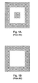
- FIGs 1A and 1B illustrate two possible BGA configurations. Each drawing illustrates a view of the BGA from the bottom side (i.e. the side that mounts to the PCB).
- the BGA shown includes a plurality of electrical contacts in a "ring" arrangement near the peripheries of the package. A plurality of electrical contacts is also located in the center of the package, with an open space in between. Typically, electrical contacts for conveying power in this type of BGA are located on the inner portion of the ring, with ground contacts located in the center.
- Figure 1B illustrates a similar BGA arrangement, minus the central group of electrical contacts.
- power and ground contacts are typically located on the inner portion of the ring.
- Both types of BGA's may be mounted to corresponding contact pads on a PCB.
- the plurality of contact pads to which a BGA is mounted is sometimes referred to as a "footprint”.
- decoupling capacitance is provided for BGA's through the use of one or more surface mounted capacitors. If the decoupling capacitors are mounted on the same side of the PCB as the BGA, they will typically be placed by some distance away from the power and ground pins of the BGA package. In such cases, a greater number of capacitors may be required to overcome the effects of ESL. As an alternative, ESL may be minimized by mounting the decoupling capacitors nearer the power and ground contacts of the BGA, but on the opposite side of the PCB. While this alternative may reduce the effects of ESL, it may add complexity to the assembly of the finished product. By placing capacitors on the opposite side of the PCB, extra soldering operations may be required. Furthermore, gluing operations to secure the capacitors to the PCB prior to soldering may be required as well. The extra manufacturing operations may result in a significant increase in the cost of the finished product, and increase the likelihood of defects during the assembly process.
- US-A-5,798,567 discloses a printed circuit board assembly where decoupling capacitors within a BGA footprint are interposed between a BGA substrate and a printed circuit board. The capacitors are soldered to contact pads on the underside of the BGA substrate.
- a printed circuit board assembly comprising: a printed circuit board (PCB), wherein said PCB includes a plurality of contact pads which form a ball grid array (BGA) footprint; a BGA package having a plurality of contacts electrically connected to said plurality of contact pads; and a capacitor package interposed between said PCB and said BGA package, characterised by said capacitor package including a first capacitor and a second capacitor, wherein the capacitance values of the first capacitor and the second capacitor differ by a factor of 10.
- PCB printed circuit board
- BGA ball grid array
- the capacitor package may have physical dimensions which allow a BGA package to be mounted such that there is no physical contact between the capacitor package and the BGA.
- the capacitor package is no more than 0.5mm in thickness.
- the thin capacitor package has no leads. Terminals located on the capacitor package may be soldered directly to the appropriate contact pads on the PCB. Since the package is leadless, equivalent series inductance (ESL) may be minimized. In some cases, the minimization of ESL may result in the need for fewer capacitors to effectively decouple a BGA package.
- ESL equivalent series inductance
- improved bypass decoupling for BGA packages may be accomplished by interposing thin capacitor packages between a BGA and a PCB.
- interposing capacitor packages between a BGA and the PCB some manufacturing operations may be eliminated which may result in cost reductions to the finished product.
- the use of leadless capacitor packages may help minimize ESL and thus allow the use of fewer capacitors to effectively decouple a BGA.
- the use of capacitor packages with multiple capacitors may allow the effective filtering of transients occurring at different frequencies.
- the use of open space under a BGA may allow for more efficient utilization of circuit board area for other components.
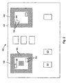
- PCA 100 includes printed circuit board (PCB) 101.
- PCB 101 includes two BGA footprints 102, each of which is formed by a plurality of contact pads 105.
- a plurality of chips 107 is mounted upon PCB 101.
- Mounted within the periphery of each BGA footprint are capacitors 103.
- Each capacitor 103 is a thin capacitor that may be interposed between a BGA and PCB 101.
- Capacitors 103 may be physically and electrically connected to PCB 101 by soldering them to additional contact pads 104, which are located within the periphery of the BGA footprint formed by contact pads 105.
- Capacitors 103 may be electrically coupled to a power distribution line at one terminal and a ground at the other terminal. In the embodiment shown, capacitors 103 do not have leads, and thus are soldered to contact pads 104 via terminals located on the body of the capacitor packaging. Capacitors 103 provide decoupling for BGA packages that may be mounted to contact pads 105 of BGA footprints 102, and may be effective in filtering out power system transients. Various alternate embodiments may use more than two capacitors per BGA (as shown in the drawing), while others may use only one.
- capacitors 103 may be mounted to PCB 101. Terminals on capacitors 103 may be soldered to contact pads 104, which are located within the periphery of BGA footprint 102 in this embodiment. Contact pads 104 are also located on the same surface of PCB 101 as contact pads 105. BGA footprint 102 is formed by a plurality of contact pads 105. In some embodiments capacitors 103 may be secured to PCB 101 by an adhesive prior to soldering. Following the placement of capacitors 103, BGA 110 may be placed on PCB 101, aligning it with contact pads 105 of BGA footprint 102.
- PCB printed circuit board
- soldering operation may be used to physically and electrically connect BGA 110 to PCB 101.
- a single soldering operation may be used to solder both BGA 110 and capacitors 103 to their respective contact pads, while separate soldering operations may be used in other embodiments.
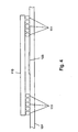
- FIG 4 is a side view of one embodiment of a thin capacitor mounted upon a PCB and interposed between a BGA and the PCB upon which it is mounted.
- Capacitor 103 may be mounted to PCB 101 as described with reference to Figure 2 and Figure 3.
- BGA 110 is also mounted to PCB 101.
- Electrical contacts 111 may be used to couple BGA 110 to PCB 101.
- each electrical contact 111 includes a pre-formed ball of solder that may be used to solder the BGA to contact pads such as those shown in Figure 2. Because of the small thickness of capacitor 103 may be mounted on the same surface as BGA 110, and thus interposed between BGA 110 and PCB 101.
- the thickness of the type of capacitors used in the embodiment shown are no more than 0.5 millimeters, and may be significantly less.
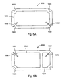
- FIGS 5A and 5B illustrate a top view and a bottom view, respectively, of one embodiment of a capacitor package 1030 that may be used in various embodiments.
- Capacitor package 1030 includes a plurality of contact terminals 1031, which may include exposed metal suitable for soldering to a contact pad on a PCB. Metal may be exposed on both sides of the terminals in some embodiments, which may allow for a more secure solder connection between the capacitor package and the contacts of the PCB.
- two of contact terminals 1031 are electrically connected to a capacitor plate 1033 by conductors 1032.
- Conductors 1032 provide an electrical connection between a contact terminal 1031 and capacitor plate 1033.
- Alternate embodiments of the capacitor package may be constructed such that a capacitor plate makes direct contact with a contact terminal, thus eliminating the need for a conductor such as that shown here.
- Capacitor plates 1034 and 1035 are shown in Figure 5B, which is a bottom view of the capacitor package 1030. Each of these capacitor plates is electrically connected to a terminal 1031 by a conductor 1032. Since there are two separate capacitor plates present on the bottom side, capacitor package 1030 essentially includes two capacitors. Each capacitor in this embodiment is a two-plate capacitor, with the capacitor plates shown in Figure 5B each forming a capacitor with capacitor plate 1033 shown in Figure 5A. The capacitor plates may be separated by a dielectric material, as will be explained in further detail below.
- capacitor package may include only a single capacitor, while others may include more than two capacitors.
- capacitor packages may include a network of several capacitors of equal capacitance, or multiple capacitors with different values of capacitance. Since the area of capacitor plate 1034 is greater than that of capacitor plate 1035, its capacitance value will also be greater as well.
- the capacitance values of two capacitors in a package may differ by a factor of 10. By decoupling in a "decade" fashion such as this, different frequencies may be filtered out when power system transients occur.
- the capacitors shown in this embodiment have a tolerance value of ⁇ 20%, although greater or lesser tolerance values may be present in other embodiments.
- Capacitor 103 is a capacitor in a standard two-plate configuration including capacitor plates 1033 and 1034. Each capacitor plate may be formed from an electrically conductive material. Capacitor plates 1033 and 1034 are separated by a dielectric layer 1036. Dielectric layer 1036 may be formed from any suitable dielectric material.
- This invention is applicable to printed circuit board assemblies, and more particularly, to the use of thin decoupling capacitors in conjunction with ball-grid array (BGA) packages.
- BGA ball-grid array
Landscapes
- Engineering & Computer Science (AREA)
- Microelectronics & Electronic Packaging (AREA)
- Physics & Mathematics (AREA)
- Electromagnetism (AREA)
- Structures For Mounting Electric Components On Printed Circuit Boards (AREA)
Applications Claiming Priority (3)
| Application Number | Priority Date | Filing Date | Title |
|---|---|---|---|
| US09/518,491 US6404649B1 (en) | 2000-03-03 | 2000-03-03 | Printed circuit board assembly with improved bypass decoupling for BGA packages |
| US518491 | 2000-03-03 | ||
| PCT/US2000/031960 WO2001067833A1 (en) | 2000-03-03 | 2000-11-21 | A printed circuit board assembly with improved bypass decoupling for bga packages |
Publications (2)
| Publication Number | Publication Date |
|---|---|
| EP1260121A1 EP1260121A1 (en) | 2002-11-27 |
| EP1260121B1 true EP1260121B1 (en) | 2006-06-21 |
Family
ID=24064157
Family Applications (1)
| Application Number | Title | Priority Date | Filing Date |
|---|---|---|---|
| EP00990918A Expired - Lifetime EP1260121B1 (en) | 2000-03-03 | 2000-11-21 | A printed circuit board assembly with improved bypass decoupling for bga packages |
Country Status (7)
| Country | Link |
|---|---|
| US (1) | US6404649B1 (enExample) |
| EP (1) | EP1260121B1 (enExample) |
| JP (1) | JP2003526221A (enExample) |
| KR (1) | KR100747130B1 (enExample) |
| CN (1) | CN1204793C (enExample) |
| DE (1) | DE60029011T2 (enExample) |
| WO (1) | WO2001067833A1 (enExample) |
Families Citing this family (18)
| Publication number | Priority date | Publication date | Assignee | Title |
|---|---|---|---|---|
| US7247932B1 (en) | 2000-05-19 | 2007-07-24 | Megica Corporation | Chip package with capacitor |
| TW502492B (en) * | 2000-05-30 | 2002-09-11 | Alps Electric Co Ltd | Electronic circuit unit |
| US6900991B2 (en) * | 2001-12-03 | 2005-05-31 | Intel Corporation | Electronic assembly with sandwiched capacitors and methods of manufacture |
| US20040000704A1 (en) * | 2002-07-01 | 2004-01-01 | George Tsao | Process for grid array assembly and electronic device made thereby |
| US7005736B2 (en) * | 2002-09-30 | 2006-02-28 | Intel Corporation | Semiconductor device power interconnect striping |
| US20040125580A1 (en) * | 2002-12-31 | 2004-07-01 | Intel Corporation | Mounting capacitors under ball grid array |
| US7153723B1 (en) | 2003-12-04 | 2006-12-26 | Emc Corporation | Method of forming a ball grid array device |
| US7235875B2 (en) * | 2004-12-09 | 2007-06-26 | International Business Machines Corporation | Modular heat sink decoupling capacitor array forming heat sink fins and power distribution interposer module |
| KR100714625B1 (ko) * | 2005-10-18 | 2007-05-07 | 삼성전기주식회사 | 박막 캐패시터 내장형 인쇄회로기판의 제조방법 |
| US7622325B2 (en) * | 2005-10-29 | 2009-11-24 | Stats Chippac Ltd. | Integrated circuit package system including high-density small footprint system-in-package |
| US8222079B2 (en) | 2007-09-28 | 2012-07-17 | International Business Machines Corporation | Semiconductor device and method of making semiconductor device |
| US7872483B2 (en) * | 2007-12-12 | 2011-01-18 | Samsung Electronics Co., Ltd. | Circuit board having bypass pad |
| US9607935B2 (en) | 2009-04-21 | 2017-03-28 | Ati Technologies Ulc | Semiconductor chip package with undermount passive devices |
| US8289727B2 (en) * | 2010-06-11 | 2012-10-16 | Taiwan Semiconductor Manufacturing Company, Ltd. | Package substrate |
| US8631706B2 (en) | 2010-07-21 | 2014-01-21 | International Business Machines Corporation | Noise suppressor for semiconductor packages |
| US9510448B2 (en) | 2014-08-29 | 2016-11-29 | Lenovo Enterprise Solutions (Singapore) Pte. Ltd. | Maximizing surface area of surface mount contact pads of circuit board also having via contact pads |
| US9769926B2 (en) * | 2015-04-23 | 2017-09-19 | Dell Products L.P. | Breakout via system |
| US11495588B2 (en) | 2018-12-07 | 2022-11-08 | Advanced Micro Devices, Inc. | Circuit board with compact passive component arrangement |
Family Cites Families (28)
| Publication number | Priority date | Publication date | Assignee | Title |
|---|---|---|---|---|
| US4734818A (en) * | 1985-01-22 | 1988-03-29 | Rogers Corporation | Decoupling capacitor for surface mounted leadless chip carriers, surface mounted leaded chip carriers and Pin Grid Array packages |
| GB2176654B (en) | 1985-06-11 | 1988-08-10 | Avx Corp | Method for optimising the decoupling of integrated circuit devices |
| US4779164A (en) * | 1986-12-12 | 1988-10-18 | Menzies Jr L William | Surface mounted decoupling capacitor |
| JPS63157919U (enExample) * | 1987-04-01 | 1988-10-17 | ||
| US4853826A (en) * | 1988-08-01 | 1989-08-01 | Rogers Corporation | Low inductance decoupling capacitor |
| US5010447A (en) * | 1988-12-28 | 1991-04-23 | Texas Instruments Incorporated | Divided capacitor mounting pads |
| US4885841A (en) * | 1989-02-21 | 1989-12-12 | Micron Technology, Inc. | Vibrational method of aligning the leads of surface-mount electronic components with the mounting pads of printed circuit boards during the molten solder mounting process |
| US5272590A (en) * | 1990-02-12 | 1993-12-21 | Hernandez Jorge M | Integrated circuit package having an internal cavity for incorporating decoupling capacitor |
| US5309324A (en) * | 1991-11-26 | 1994-05-03 | Herandez Jorge M | Device for interconnecting integrated circuit packages to circuit boards |
| KR0134648B1 (ko) * | 1994-06-09 | 1998-04-20 | 김광호 | 노이즈가 적은 적층 멀티칩 패키지 |
| JPH0982557A (ja) | 1995-09-18 | 1997-03-28 | Canon Inc | バイパスコンデンサ |
| JPH09102432A (ja) | 1995-10-05 | 1997-04-15 | Canon Inc | バイパスコンデンサ及びその形成方法 |
| JPH09130031A (ja) * | 1995-10-27 | 1997-05-16 | Hitachi Ltd | 電子部品の実装方法 |
| JPH09223861A (ja) | 1996-02-19 | 1997-08-26 | Canon Inc | 半導体集積回路及びプリント配線基板 |
| US5654676A (en) * | 1996-06-10 | 1997-08-05 | Motorola, Inc. | Shielded VCO module having trimmable capacitor plate external to shield |
| US5751555A (en) * | 1996-08-19 | 1998-05-12 | Motorola, Inc. | Electronic component having reduced capacitance |
| JPH1084011A (ja) | 1996-09-06 | 1998-03-31 | Hitachi Ltd | 半導体装置及びこの製造方法並びにその実装方法 |
| US5841686A (en) * | 1996-11-22 | 1998-11-24 | Ma Laboratories, Inc. | Dual-bank memory module with shared capacitors and R-C elements integrated into the module substrate |
| JP2845227B2 (ja) * | 1996-11-29 | 1999-01-13 | 日本電気株式会社 | マルチチップモジュールの実装構造 |
| KR19980084427A (ko) * | 1997-05-23 | 1998-12-05 | 김영환 | 패키지장치의 내장형 바이패스 커패시터 |
| US5798567A (en) * | 1997-08-21 | 1998-08-25 | Hewlett-Packard Company | Ball grid array integrated circuit package which employs a flip chip integrated circuit and decoupling capacitors |
| US6272020B1 (en) * | 1997-10-16 | 2001-08-07 | Hitachi, Ltd. | Structure for mounting a semiconductor device and a capacitor device on a substrate |
| JPH11121899A (ja) * | 1997-10-20 | 1999-04-30 | Fuji Xerox Co Ltd | 電子部品実装体および電子部品の実装方法 |
| US5939782A (en) * | 1998-03-03 | 1999-08-17 | Sun Microsystems, Inc. | Package construction for integrated circuit chip with bypass capacitor |
| JPH11260999A (ja) * | 1998-03-13 | 1999-09-24 | Sumitomo Metal Ind Ltd | ノイズを低減した積層半導体装置モジュール |
| US5973928A (en) * | 1998-08-18 | 1999-10-26 | International Business Machines Corporation | Multi-layer ceramic substrate decoupling |
| US6144559A (en) * | 1999-04-08 | 2000-11-07 | Agilent Technologies | Process for assembling an interposer to probe dense pad arrays |
| JP4484176B2 (ja) * | 2000-01-21 | 2010-06-16 | イビデン株式会社 | ボールグリッドアレイ型パッケージの接続構造 |
-
2000
- 2000-03-03 US US09/518,491 patent/US6404649B1/en not_active Expired - Lifetime
- 2000-11-21 DE DE60029011T patent/DE60029011T2/de not_active Expired - Lifetime
- 2000-11-21 CN CNB008192111A patent/CN1204793C/zh not_active Expired - Lifetime
- 2000-11-21 WO PCT/US2000/031960 patent/WO2001067833A1/en not_active Ceased
- 2000-11-21 JP JP2001565717A patent/JP2003526221A/ja active Pending
- 2000-11-21 KR KR1020027011585A patent/KR100747130B1/ko not_active Expired - Lifetime
- 2000-11-21 EP EP00990918A patent/EP1260121B1/en not_active Expired - Lifetime
Also Published As
| Publication number | Publication date |
|---|---|
| WO2001067833A1 (en) | 2001-09-13 |
| CN1204793C (zh) | 2005-06-01 |
| KR20020082865A (ko) | 2002-10-31 |
| CN1437839A (zh) | 2003-08-20 |
| JP2003526221A (ja) | 2003-09-02 |
| US6404649B1 (en) | 2002-06-11 |
| DE60029011T2 (de) | 2007-01-11 |
| EP1260121A1 (en) | 2002-11-27 |
| DE60029011D1 (de) | 2006-08-03 |
| KR100747130B1 (ko) | 2007-08-09 |
Similar Documents
| Publication | Publication Date | Title |
|---|---|---|
| EP1260121B1 (en) | A printed circuit board assembly with improved bypass decoupling for bga packages | |
| US5708296A (en) | Power-ground plane for a C4 flip-chip substrate | |
| US6084779A (en) | Ground and power patches on printed circuit board signal planes in the areas of integrated circuit chips | |
| US6043559A (en) | Integrated circuit package which contains two in plane voltage busses and a wrap around conductive strip that connects a bond finger to one of the busses | |
| US5834832A (en) | Packing structure of semiconductor packages | |
| US6730860B2 (en) | Electronic assembly and a method of constructing an electronic assembly | |
| KR20040015760A (ko) | 수직 접속된 캐패시터를 구비하는 전자 어셈블리 및 제조방법 | |
| US20220007499A1 (en) | Module, terminal assembly, and method for producing module | |
| US20040125580A1 (en) | Mounting capacitors under ball grid array | |
| KR100543853B1 (ko) | 확장 표면 랜드를 갖는 커패시터 및 그 제조 방법 | |
| US6933597B1 (en) | Spacer with passive components for use in multi-chip modules | |
| US6636416B2 (en) | Electronic assembly with laterally connected capacitors and manufacturing method | |
| US4402561A (en) | Socket for integrated circuit package with extended leads | |
| CA1188010A (en) | Package for a semiconductor chip | |
| US4449770A (en) | Socketless separable connector | |
| WO1998010466A1 (en) | An integrated circuit package | |
| CN212113714U (zh) | 射频前端模组、射频通信装置和电子设备 | |
| US5006963A (en) | Selectable chip carrier | |
| US7221046B2 (en) | System to control effective series resistance of power delivery circuit | |
| EP1604401B1 (en) | Semiconductor device, semiconductor body and method of manufacturing thereof | |
| EP1111969B1 (en) | Method and structure for reducing power noise | |
| US20050280134A1 (en) | Multi-frequency noise suppression capacitor set | |
| JPH04192353A (ja) | 集積回路 | |
| JPH08340059A (ja) | 半導体デバイスパッケージングシステム | |
| JPS62188256A (ja) | 集積回路チツプ |
Legal Events
| Date | Code | Title | Description |
|---|---|---|---|
| PUAI | Public reference made under article 153(3) epc to a published international application that has entered the european phase |
Free format text: ORIGINAL CODE: 0009012 |
|
| 17P | Request for examination filed |
Effective date: 20020809 |
|
| AK | Designated contracting states |
Kind code of ref document: A1 Designated state(s): AT BE CH CY DE DK ES FI FR GB GR IE IT LI LU MC NL PT SE TR |
|
| RIN1 | Information on inventor provided before grant (corrected) |
Inventor name: SCHELLING, GREG Inventor name: DRAKE, MICHAEL Inventor name: GUERRERO, EDWARD Inventor name: BENNETT, JOHN Inventor name: TRESSLER, CHRIS |
|
| RBV | Designated contracting states (corrected) |
Designated state(s): AT BE DE GB |
|
| GRAP | Despatch of communication of intention to grant a patent |
Free format text: ORIGINAL CODE: EPIDOSNIGR1 |
|
| GRAS | Grant fee paid |
Free format text: ORIGINAL CODE: EPIDOSNIGR3 |
|
| GRAA | (expected) grant |
Free format text: ORIGINAL CODE: 0009210 |
|
| AK | Designated contracting states |
Kind code of ref document: B1 Designated state(s): DE GB |
|
| RBV | Designated contracting states (corrected) |
Designated state(s): DE GB |
|
| REG | Reference to a national code |
Ref country code: GB Ref legal event code: FG4D |
|
| REF | Corresponds to: |
Ref document number: 60029011 Country of ref document: DE Date of ref document: 20060803 Kind code of ref document: P |
|
| PLBE | No opposition filed within time limit |
Free format text: ORIGINAL CODE: 0009261 |
|
| STAA | Information on the status of an ep patent application or granted ep patent |
Free format text: STATUS: NO OPPOSITION FILED WITHIN TIME LIMIT |
|
| 26N | No opposition filed |
Effective date: 20070322 |
|
| PGFP | Annual fee paid to national office [announced via postgrant information from national office to epo] |
Ref country code: DE Payment date: 20191105 Year of fee payment: 20 |
|
| PGFP | Annual fee paid to national office [announced via postgrant information from national office to epo] |
Ref country code: GB Payment date: 20191122 Year of fee payment: 20 |
|
| REG | Reference to a national code |
Ref country code: DE Ref legal event code: R071 Ref document number: 60029011 Country of ref document: DE |
|
| REG | Reference to a national code |
Ref country code: GB Ref legal event code: PE20 Expiry date: 20201120 |
|
| PG25 | Lapsed in a contracting state [announced via postgrant information from national office to epo] |
Ref country code: GB Free format text: LAPSE BECAUSE OF EXPIRATION OF PROTECTION Effective date: 20201120 |