EP1111969B1 - Method and structure for reducing power noise - Google Patents
Method and structure for reducing power noise Download PDFInfo
- Publication number
- EP1111969B1 EP1111969B1 EP00126690A EP00126690A EP1111969B1 EP 1111969 B1 EP1111969 B1 EP 1111969B1 EP 00126690 A EP00126690 A EP 00126690A EP 00126690 A EP00126690 A EP 00126690A EP 1111969 B1 EP1111969 B1 EP 1111969B1
- Authority
- EP
- European Patent Office
- Prior art keywords
- capacitors
- pads
- capacitor
- vias
- decoupling
- Prior art date
- Legal status (The legal status is an assumption and is not a legal conclusion. Google has not performed a legal analysis and makes no representation as to the accuracy of the status listed.)
- Expired - Lifetime
Links
Images


Classifications
-
- H—ELECTRICITY
- H05—ELECTRIC TECHNIQUES NOT OTHERWISE PROVIDED FOR
- H05K—PRINTED CIRCUITS; CASINGS OR CONSTRUCTIONAL DETAILS OF ELECTRIC APPARATUS; MANUFACTURE OF ASSEMBLAGES OF ELECTRICAL COMPONENTS
- H05K1/00—Printed circuits
- H05K1/02—Details
- H05K1/11—Printed elements for providing electric connections to or between printed circuits
- H05K1/111—Pads for surface mounting, e.g. lay-out
- H05K1/112—Pads for surface mounting, e.g. lay-out directly combined with via connections
- H05K1/113—Via provided in pad; Pad over filled via
-
- H—ELECTRICITY
- H05—ELECTRIC TECHNIQUES NOT OTHERWISE PROVIDED FOR
- H05K—PRINTED CIRCUITS; CASINGS OR CONSTRUCTIONAL DETAILS OF ELECTRIC APPARATUS; MANUFACTURE OF ASSEMBLAGES OF ELECTRICAL COMPONENTS
- H05K1/00—Printed circuits
- H05K1/02—Details
- H05K1/0213—Electrical arrangements not otherwise provided for
- H05K1/0216—Reduction of cross-talk, noise or electromagnetic interference
- H05K1/023—Reduction of cross-talk, noise or electromagnetic interference using auxiliary mounted passive components or auxiliary substances
- H05K1/0231—Capacitors or dielectric substances
-
- H—ELECTRICITY
- H05—ELECTRIC TECHNIQUES NOT OTHERWISE PROVIDED FOR
- H05K—PRINTED CIRCUITS; CASINGS OR CONSTRUCTIONAL DETAILS OF ELECTRIC APPARATUS; MANUFACTURE OF ASSEMBLAGES OF ELECTRICAL COMPONENTS
- H05K1/00—Printed circuits
- H05K1/02—Details
- H05K1/11—Printed elements for providing electric connections to or between printed circuits
- H05K1/115—Via connections; Lands around holes or via connections
-
- H—ELECTRICITY
- H05—ELECTRIC TECHNIQUES NOT OTHERWISE PROVIDED FOR
- H05K—PRINTED CIRCUITS; CASINGS OR CONSTRUCTIONAL DETAILS OF ELECTRIC APPARATUS; MANUFACTURE OF ASSEMBLAGES OF ELECTRICAL COMPONENTS
- H05K2201/00—Indexing scheme relating to printed circuits covered by H05K1/00
- H05K2201/09—Shape and layout
- H05K2201/09209—Shape and layout details of conductors
- H05K2201/09654—Shape and layout details of conductors covering at least two types of conductors provided for in H05K2201/09218 - H05K2201/095
- H05K2201/0979—Redundant conductors or connections, i.e. more than one current path between two points
-
- H—ELECTRICITY
- H05—ELECTRIC TECHNIQUES NOT OTHERWISE PROVIDED FOR
- H05K—PRINTED CIRCUITS; CASINGS OR CONSTRUCTIONAL DETAILS OF ELECTRIC APPARATUS; MANUFACTURE OF ASSEMBLAGES OF ELECTRICAL COMPONENTS
- H05K2201/00—Indexing scheme relating to printed circuits covered by H05K1/00
- H05K2201/10—Details of components or other objects attached to or integrated in a printed circuit board
- H05K2201/10431—Details of mounted components
- H05K2201/10507—Involving several components
- H05K2201/10522—Adjacent components
-
- H—ELECTRICITY
- H05—ELECTRIC TECHNIQUES NOT OTHERWISE PROVIDED FOR
- H05K—PRINTED CIRCUITS; CASINGS OR CONSTRUCTIONAL DETAILS OF ELECTRIC APPARATUS; MANUFACTURE OF ASSEMBLAGES OF ELECTRICAL COMPONENTS
- H05K2201/00—Indexing scheme relating to printed circuits covered by H05K1/00
- H05K2201/10—Details of components or other objects attached to or integrated in a printed circuit board
- H05K2201/10613—Details of electrical connections of non-printed components, e.g. special leads
- H05K2201/10621—Components characterised by their electrical contacts
- H05K2201/10636—Leadless chip, e.g. chip capacitor or resistor
-
- H—ELECTRICITY
- H05—ELECTRIC TECHNIQUES NOT OTHERWISE PROVIDED FOR
- H05K—PRINTED CIRCUITS; CASINGS OR CONSTRUCTIONAL DETAILS OF ELECTRIC APPARATUS; MANUFACTURE OF ASSEMBLAGES OF ELECTRICAL COMPONENTS
- H05K3/00—Apparatus or processes for manufacturing printed circuits
- H05K3/40—Forming printed elements for providing electric connections to or between printed circuits
- H05K3/42—Plated through-holes or plated via connections
- H05K3/429—Plated through-holes specially for multilayer circuits, e.g. having connections to inner circuit layers
-
- Y—GENERAL TAGGING OF NEW TECHNOLOGICAL DEVELOPMENTS; GENERAL TAGGING OF CROSS-SECTIONAL TECHNOLOGIES SPANNING OVER SEVERAL SECTIONS OF THE IPC; TECHNICAL SUBJECTS COVERED BY FORMER USPC CROSS-REFERENCE ART COLLECTIONS [XRACs] AND DIGESTS
- Y02—TECHNOLOGIES OR APPLICATIONS FOR MITIGATION OR ADAPTATION AGAINST CLIMATE CHANGE
- Y02P—CLIMATE CHANGE MITIGATION TECHNOLOGIES IN THE PRODUCTION OR PROCESSING OF GOODS
- Y02P70/00—Climate change mitigation technologies in the production process for final industrial or consumer products
- Y02P70/50—Manufacturing or production processes characterised by the final manufactured product
Definitions
- the present invention relates in general to the reduction of power noise. In particular, it relates to such a reduction in the mid- and high-frequency range. Still more specifically, the invention relates to a pad-via configuration for SMT decoupling capacitors.
- the charge of the capacitors must be provided as fast as possible to the noise source. Therefore the internal inductance of the capacitor as well as the path inductance (capacitor to noise source) must be kept as small as possible. Due to these restrictions the capacitor must be
- Decoupling capacitors are used to provide a short term current source or sink for the circuitry in an effort to provide a stable power supply.
- the decoupling capacitors act as a storage device for electrical charge which can provide a short term current source for the circuitry.
- capacitors with a low capacitance value may be used as a high frequency noise filter, and capacitors with a high capacity value may be used as a low frequency noise filter.
- US-A-4,654,694 discloses side connections to place a capacitor in close proximity to a chip or, alternatively, to a chip and GND/Power I/O. By this technique, the effective inductance of the power paths is minimized.
- US-A-4,945,399 describes a semiconductor chip carrier including a plurality of distributed high frequency decoupling capacitors as an integral part of the carrier.
- the distributed capacitors are formed as a part of the first and second layers of metallurgy and separated by a layer of thin film dielectric material.
- US-A-5,132,613 discloses an integrated circuit test structure including individual layers of a personalization substrate and decoupling capacitors, whereby said decoupling capacitors are electrically coupled to the metal lines in close proximity, the personalization substrate thereby minimizing the associated lead inductance and thus maximizing the effectiveness of the decoupling capacitors.
- US-A-5,731,960 describes a noise-suppression apparatus for a PCB comprising a decoupling capacitor coupled to mounting regions of pads also having a boundary region connected to vias.
- Figure 1 the common pad and via design (as normally recommended by the capacitor vendor) is shown as a top view drawing in combination with one mounted capacitor.
- Figure 2 shows the same pad and via configuration with the mounted capacitor in a three-dimensional view.
- the size of the pad 2 itself is mainly driven by the size of the capacitor body 4 and by manufacturing especially soldering recommendations.
- the vias 6 are placed outside the soldering area 8 of the pad.
- the center to center distance "D" of the vias is large.
- Each pad 2 of the capacitor 4 is connected with a via 6 to power and ground respectively (not shown).
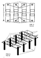
- Figure 3 shows a two-dimensional and figure 4 a three-dimensional drawing of multiple capacitor pads 2 with vias 6 and mounted capacitors 4.
- the new capacitor pad and via configuration according to the invention is shown in figures 5 and 6, respectively.
- the main differences between the old pad via configuration as shown in figures 1 and 2 are the pad size, the distance between both pads and the via location and thus also the center to center distance "D" of the vias 6.
- the pads are now enlarged in, the vias thereby being arranged in close proximity to the respective capacitors.
- the pad via configuration has to meet the following requirements:
- a further reduction of the loop inductance of the pad via configuration as shown in Figures 5 and 6 can be achieved by:
- capacitors In order to use multiple surface mount capacitors for decoupling purposes of one voltage the capacitors can be mounted on capacitor pad lines as shown in Figures 7 and 8.
- the distances "B" between the capacitor bodies remain the same as in Figs. 3 and 4, being determined mainly by the assembly tool used.
- the vias 6 are placed in the area between the capacitors 4 with a minimum center to center distance "D" of a via pair.
- the distance "P” between the pad lines is also reduced to a minimum.
- FIG. 9 A further improvement of this structure is shown in Figures 9 and 10 where the width of the pad 2 line is enlarged and an additional via pair 6a is added at the outer ends of the pad line 2.
- the pad line distance under the capacitor can be enlarged.
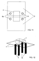
- a further improvement can be achieved if the pads 2 of figure 5 are enlarged so that an additional via pair 6b can be placed on the outer side of capacitor 4.
- This embodiment is shown in figs. 11 and 12.
- Figure 13 shows a comparision of the simulated loop inductance for a group of three capacitors using seperate pads (old design) and the pad line structure (new design) with 18mils via diameter and for different via lengths.
- the total loop inductance can by reduced by a factor of 5.3 for a via with a length of 500 ⁇ m and by a factor of 2.7 for via with a length of 2.5mm.
- Another main advantage of the new pad via design is the improved wireability in the capacitor area.
- Each via is fabricated with clearence holes on each power layer (for a via connected to ground) and on each ground layer (for a via connected to power). Due to different reasons (e.g. coupling, impedance mismatch) signal wires are in general not allowed to cross a clearence hole. Thus the clearence hole reduces the wireability in the capacitor area.
- the via holes of the new capacitor pad-via design are overlapping due to the small distance between the via pair. Due to the overlap of the via holes the wiring area is increased.
- the wireability in the capacitor area is increased, the number of wire layers can be reduced in a dense wiring area and at last the card and board costs can be reduced.
Description
- The present invention relates in general to the reduction of power noise. In particular, it relates to such a reduction in the mid- and high-frequency range. Still more specifically, the invention relates to a pad-via configuration for SMT decoupling capacitors.
- Due to the growing complexity of semiconductor devices the total amount of switching current needed by the logic devices increases. As a result the simultaneous switching noise increases also and results in a slower working logic, in a slower cycle time and thus in a decreasing system performance. In order to yield a higher system performance one goal of modern system designs is to stabilize the voltage. It is known that a stabilized voltage can be obtained with the help of decoupling capacitors mounted on MCMs, cards and boards. However, the higher power noise combined with a lower operating voltage of the semiconductor devices results in a growing number of capacitors needed for decoupling purposes. This results in additional problems:
- large areas on MCM, cards and/or boards needed for capacitor placement and with a growing distance of the capacitor to the noise source the effectiveness of the capacitor is decreased
- reduced placement area for capacitors, due to a higher component integration factor on cards/boards
- growing costs for assembled components, due to a higher number of components and increase of manufacturing time (drilling of via holes, component placement, edging, etc.)
- wiring problems on cards/boards, due to an increased number of power/ground vias as well as a possibly increased signal delay, decreased cycle time, increased number of card/board layers and decreased system performance
- decreased effective copper on power and ground layers, due to an increased number of via and clearence holes; increased DC resistance of power and ground planes; increased DC voltage drop on card/board between voltage source and logic; decreased system performance.
- In order to make all the capacitors as effective as possible the charge of the capacitors must be provided as fast as possible to the noise source. Therefore the internal inductance of the capacitor as well as the path inductance (capacitor to noise source) must be kept as small as possible. Due to these restrictions the capacitor must
- be placed as close as possible to the noise source;
- have a small internal inductance; and
- have a small inductance of the capacitor pad and the via connecting the pad to the voltage and ground plane.
- Decoupling capacitors are used to provide a short term current source or sink for the circuitry in an effort to provide a stable power supply. For example, the decoupling capacitors act as a storage device for electrical charge which can provide a short term current source for the circuitry.
- It is well known in the art that capacitors with a low capacitance value may be used as a high frequency noise filter, and capacitors with a high capacity value may be used as a low frequency noise filter.
- Typically, decoupling capacitors are placed as close as possible to the circuitry so as to increase their effectiveness. Thus,
US-A-4,654,694 discloses side connections to place a capacitor in close proximity to a chip or, alternatively, to a chip and GND/Power I/O. By this technique, the effective inductance of the power paths is minimized. - In some instances, decoupling capacitors have been placed within the package containing the integrated circuit. Thus,
US-A-4,945,399 describes a semiconductor chip carrier including a plurality of distributed high frequency decoupling capacitors as an integral part of the carrier. The distributed capacitors are formed as a part of the first and second layers of metallurgy and separated by a layer of thin film dielectric material. -
US-A-5,132,613 discloses an integrated circuit test structure including individual layers of a personalization substrate and decoupling capacitors, whereby said decoupling capacitors are electrically coupled to the metal lines in close proximity, the personalization substrate thereby minimizing the associated lead inductance and thus maximizing the effectiveness of the decoupling capacitors. - Although there are some advantages in using capacitors with a low internal inductance, a great disadvantage is the also low capacitance of the capacitor itself (low inductance is only available with low capacitance). One further disadvantage is the decreased effectiveness of the low inductive capacitor that is limited by the inductance of the mounting pads together with the vias of the capacitor.
-
US-A-5,731,960 describes a noise-suppression apparatus for a PCB comprising a decoupling capacitor coupled to mounting regions of pads also having a boundary region connected to vias. - It is therefore an object of the present invention to provide a method for minimizing switching noise in the high- and mid-frequency range on printed circuit cards or boards by means of several surface mount decoupling capacitors, whereby the parasitic inductance of the pads and vias is minimized.
- It is a further object of the present invention to increase the effectiveness of the decoupling capacitors, to reduce the voltage drop and to increase the overall system performance.
- These and other objects and advantages are achieved by a method for minimizing switching noise in the high- and mid-frequency range according to claim 1 and by the structure of
claim 4. - Advantageous embodiments of the method according to the invention are laid down in the dependent claims.
-
- Fig. 1
- shows the common pad and via design according to the state of the art;
- Fig. 2
- depicts the design according to Fig. 1 in a three-dimensional view;
- Fig. 3
- is a two-dimensional view of multiple capacitor pads with vias and mounted capacitors according to the state of the art;
- Fig. 4
- shows the arrangement of Fig. 3 in a three-dimensional view;
- Fig. 5
- is a two-dimensional view of the capacitor pad and via configuration according to the invention;
- Fig. 6
- depicts the configuration of Fig. 5 in a three-dimensional view;
- Figs.7 and 8
- show another configuration according to the invention, providing multiple decoupling capacitors;
- Figs. 9 and 10
- show still another configuration according to the invention;
- Figs. 11 and 12
- show yet another configuration according to invention; and
- Fig. 13
- is a graph showing a comparison of the simulated loop inductance for a group of three capacitors using state of the art configuration and the configuration according to the invention.
- In Figure 1 the common pad and via design (as normally recommended by the capacitor vendor) is shown as a top view drawing in combination with one mounted capacitor. Figure 2 shows the same pad and via configuration with the mounted capacitor in a three-dimensional view. The size of the
pad 2 itself is mainly driven by the size of thecapacitor body 4 and by manufacturing especially soldering recommendations. As recommended thevias 6 are placed outside thesoldering area 8 of the pad. As shown in figure 1 and 2 the center to center distance "D" of the vias is large. Eachpad 2 of thecapacitor 4 is connected with a via 6 to power and ground respectively (not shown). - In order to be able to use multiple surface mount capacitors the capacitors are mounted side by side on pads with a safety distance which is specified by automatic placement restrictions. Figure 3 shows a two-dimensional and figure 4 a three-dimensional drawing of
multiple capacitor pads 2 withvias 6 and mountedcapacitors 4. - The new capacitor pad and via configuration according to the invention is shown in figures 5 and 6, respectively. The main differences between the old pad via configuration as shown in figures 1 and 2 are the pad size, the distance between both pads and the via location and thus also the center to center distance "D" of the
vias 6. As compared to the state of the art, the pads are now enlarged in, the vias thereby being arranged in close proximity to the respective capacitors. In order to minimize the loop inductance of the pads and vias the pad via configuration has to meet the following requirements: - minimum center to center distance "D" of the
vias 6
The reason is that the smaller the distance the higher the mutual coupling between the vias and the lower the loop inductance - minimum distance P" between both
capacitor pads 2
The reason is that the smaller the distance between the pads the smaller the distance of the vias - minmum distance "C" between the center of
vias 6 and the contact point between thecapacitor 4 and thepad 2
The reason is that the smaller the distance the smaller the loop inductance. - A further reduction of the loop inductance of the pad via configuration as shown in Figures 5 and 6 can be achieved by:
- 1. enlarging the width of the
pad 2 and adding a second via pair on the left side of the capacitor (cf. Figs. 11 and 12), so that a structure results wherein vias and capacitors are arranged alternatingly;
Thus, by paralleling the vias, the inductance L is decreased. - 2. using multiple vias on one pad in a row;
Here, paralleling the vias leads to a decrease in required floor space compared to 1. - 3. using a larger via diameter;
- 4. using a larger pad size;
Points - 5. placing the vias under the capacitor body;
- This, as well as
point 2, results in a decrease in rquired floor space and the minimum space leads to a minimum inductance. - In order to use multiple surface mount capacitors for decoupling purposes of one voltage the capacitors can be mounted on capacitor pad lines as shown in Figures 7 and 8. The distances "B" between the capacitor bodies remain the same as in Figs. 3 and 4, being determined mainly by the assembly tool used. The
vias 6 are placed in the area between thecapacitors 4 with a minimum center to center distance "D" of a via pair. The distance "P" between the pad lines is also reduced to a minimum. - A further improvement of this structure is shown in Figures 9 and 10 where the width of the
pad 2 line is enlarged and an additional viapair 6a is added at the outer ends of thepad line 2. In order to avoid shorts between the pads caused by capacitors which are placed incorrectly, the pad line distance under the capacitor can be enlarged. - A further improvement can be achieved if the
pads 2 of figure 5 are enlarged so that an additional viapair 6b can be placed on the outer side ofcapacitor 4. This embodiment is shown in figs. 11 and 12. - Figure 13 shows a comparision of the simulated loop inductance for a group of three capacitors using seperate pads (old design) and the pad line structure (new design) with 18mils via diameter and for different via lengths. Depending of the via length the total loop inductance can by reduced by a factor of 5.3 for a via with a length of 500µm and by a factor of 2.7 for via with a length of 2.5mm.
- Due to the reduction of the pad-via loop inductance the effectiveness of the capacitor is increased and the total number of capacitors needed for decoupling purposes on cards and boards can be reduced. In table 1 a comparision of the numbers of capacitors, needed for decoupling of the 1.5V and of the 1.8V on a board, is shown as an example. The calculations were performed using the old pad via design and the new pad via design. The number of capacitors used for 1.5V and 1.8V decoupling can be reduced from 4792 to 1985 and from 373 to 155.
Table 1 Old Design New Design Capacitor # on 1.5V 4792 1985 Capacitor # on 1.8V 373 155 Capacitor # total 5165 2140 - The advantages of these reductions are:
- decreasing prices for assembled components due to decreasing component number
- reduce manufacturing cost due to reduced production cycle time (reduced component placement time and reduced drilling time for vias)
- reduce wireability problems due to reduced capacitor number and via number
- reduce component placement problems on dense assembled cards and boards
- reduce component distances due to lower number of capacitors
- reduce signal delay, reduce cycle time, increase system performance
- improve card/board cross section due to lower via number
- reduce parallel resonances between different types of capacitors due to lower parasitic inductance of the vias
- Another main advantage of the new pad via design is the improved wireability in the capacitor area. Each via is fabricated with clearence holes on each power layer (for a via connected to ground) and on each ground layer (for a via connected to power). Due to different reasons (e.g. coupling, impedance mismatch) signal wires are in general not allowed to cross a clearence hole. Thus the clearence hole reduces the wireability in the capacitor area. In contrast to the old capacitor pad-via design were the clearence holes of a via pair (power and ground via of one capacitor) are seperated, the via holes of the new capacitor pad-via design are overlapping due to the small distance between the via pair. Due to the overlap of the via holes the wiring area is increased. Thus the wireability in the capacitor area is increased, the number of wire layers can be reduced in a dense wiring area and at last the card and board costs can be reduced.
Claims (6)
- Method for minimizing switching noise in the high- and mid-frequency range on printed circuit cards or boards by means of a plurality of surface mounted decoupling capacitors (4), said capacitors each comprising a pair of opposing pads (2), each of said pads being connected to power/ground planes by respective vias (6),
characterized by the steps of
arranging said pairs of capacitor pads by connecting pads to form enlarged padlines (2) and at the same time minimizing the distance (P) between opposite pads, and arranging said respective vias (6) at the smallest possible center to center distance (D) with respect to each other and, with respect to respective decoupling capacitors, at the smallest distance (C) between the via (6) center and the contact point between the respective decoupling capacitor (4) and the pad (2). - Method according to claim 1, wherein said respective vias are arranged at only one side of the decoupling capacitor power/ground planes.
- Method according to claim 1, wherein said respective vias are arranged on both sides of the decoupling capacitor power/ground planes.
- A structure including- a printed circuit card or board,- a plurality of decoupling capacitors (4) mounted on the surface of said card or board, each of said capacitors consisting of a pair of opposing pads (2), said pads being connected to power/ground planes by respective vias (6)characterized in that
said pairs of capacitor pads are arranged to form enlarged padlines (2), and at the same time are arranged at the smallest distance (P) between opposite pads, and that said respective vias (6) are arranged at the smallest possible center to center distance (D) with respect to each other and, with respect to respective decoupling capacitors, at the smallest distance (C) between the via (6) center and the contact point between the respective decoupling capacitor (4) and the pad (2). - Structure according to claim 4 wherein said respective vias are arranged at only one side of the decoupling capacitor power/ground planes.
- Structure according to claim 4 wherein said respective vias are arranged on both sides of the decoupling capacitor power/ground planes.
Priority Applications (1)
| Application Number | Priority Date | Filing Date | Title |
|---|---|---|---|
| EP00126690A EP1111969B1 (en) | 1999-12-21 | 2000-12-05 | Method and structure for reducing power noise |
Applications Claiming Priority (3)
| Application Number | Priority Date | Filing Date | Title |
|---|---|---|---|
| EP99125462 | 1999-12-21 | ||
| EP99125462 | 1999-12-21 | ||
| EP00126690A EP1111969B1 (en) | 1999-12-21 | 2000-12-05 | Method and structure for reducing power noise |
Publications (2)
| Publication Number | Publication Date |
|---|---|
| EP1111969A1 EP1111969A1 (en) | 2001-06-27 |
| EP1111969B1 true EP1111969B1 (en) | 2008-02-06 |
Family
ID=26071643
Family Applications (1)
| Application Number | Title | Priority Date | Filing Date |
|---|---|---|---|
| EP00126690A Expired - Lifetime EP1111969B1 (en) | 1999-12-21 | 2000-12-05 | Method and structure for reducing power noise |
Country Status (1)
| Country | Link |
|---|---|
| EP (1) | EP1111969B1 (en) |
Families Citing this family (2)
| Publication number | Priority date | Publication date | Assignee | Title |
|---|---|---|---|---|
| US7614141B2 (en) | 2006-02-16 | 2009-11-10 | International Business Machines Corporation | Fabricating substrates having low inductance via arrangements |
| CN104133962A (en) * | 2014-07-29 | 2014-11-05 | 浪潮电子信息产业股份有限公司 | Via hole design method for improving capacitor decoupling effect |
Family Cites Families (4)
| Publication number | Priority date | Publication date | Assignee | Title |
|---|---|---|---|---|
| US5493259A (en) * | 1992-10-13 | 1996-02-20 | The Whitaker Corporation | High voltage, low pass filtering connector with multiple ground planes |
| US5375035A (en) * | 1993-03-22 | 1994-12-20 | Compaq Computer Corporation | Capacitor mounting structure for printed circuit boards |
| US5731960A (en) * | 1996-09-19 | 1998-03-24 | Bay Networks, Inc. | Low inductance decoupling capacitor arrangement |
| DE19642929A1 (en) * | 1996-10-17 | 1997-07-17 | Siemens Ag | Multi-layered printed circuit board with HF component |
-
2000
- 2000-12-05 EP EP00126690A patent/EP1111969B1/en not_active Expired - Lifetime
Also Published As
| Publication number | Publication date |
|---|---|
| EP1111969A1 (en) | 2001-06-27 |
Similar Documents
| Publication | Publication Date | Title |
|---|---|---|
| US5903050A (en) | Semiconductor package having capacitive extension spokes and method for making the same | |
| US6346743B1 (en) | Embedded capacitor assembly in a package | |
| US6084779A (en) | Ground and power patches on printed circuit board signal planes in the areas of integrated circuit chips | |
| US6907658B2 (en) | Manufacturing methods for an electronic assembly with vertically connected capacitors | |
| US6713860B2 (en) | Electronic assembly and system with vertically connected capacitors | |
| JP4273098B2 (en) | Multilayer printed circuit board | |
| US7355836B2 (en) | Array capacitor for decoupling multiple voltage rails | |
| CN1985550A (en) | Reducing loadline impedance in a system | |
| CN100550369C (en) | Has array capacitor in order to the space of realizing full-grid socket | |
| US7586756B2 (en) | Split thin film capacitor for multiple voltages | |
| US11387226B2 (en) | Chip power supply system, chip, PCB, and computer device | |
| US20040125580A1 (en) | Mounting capacitors under ball grid array | |
| US6636416B2 (en) | Electronic assembly with laterally connected capacitors and manufacturing method | |
| KR100308872B1 (en) | Multi-Layered Multi-chip Module | |
| US6437252B2 (en) | Method and structure for reducing power noise | |
| US7818704B1 (en) | Capacitive decoupling method and module | |
| EP1111969B1 (en) | Method and structure for reducing power noise | |
| CN100539112C (en) | Optimization is to electric power transfer high-speed, the high pin counting apparatus |
Legal Events
| Date | Code | Title | Description |
|---|---|---|---|
| PUAI | Public reference made under article 153(3) epc to a published international application that has entered the european phase |
Free format text: ORIGINAL CODE: 0009012 |
|
| AK | Designated contracting states |
Kind code of ref document: A1 Designated state(s): AT BE CH CY DE DK ES FI FR GB GR IE IT LI LU MC NL PT SE TR |
|
| AX | Request for extension of the european patent |
Free format text: AL;LT;LV;MK;RO;SI |
|
| 17P | Request for examination filed |
Effective date: 20010928 |
|
| AKX | Designation fees paid |
Free format text: AT BE CH CY DE DK ES FI FR GB GR IE IT LI LU MC NL PT SE TR |
|
| GRAP | Despatch of communication of intention to grant a patent |
Free format text: ORIGINAL CODE: EPIDOSNIGR1 |
|
| GRAS | Grant fee paid |
Free format text: ORIGINAL CODE: EPIDOSNIGR3 |
|
| GRAA | (expected) grant |
Free format text: ORIGINAL CODE: 0009210 |
|
| AK | Designated contracting states |
Kind code of ref document: B1 Designated state(s): AT BE CH CY DE DK ES FI FR GB GR IE IT LI LU MC NL PT SE TR |
|
| REG | Reference to a national code |
Ref country code: GB Ref legal event code: FG4D |
|
| REG | Reference to a national code |
Ref country code: CH Ref legal event code: EP Ref country code: CH Ref legal event code: NV Representative=s name: IBM RESEARCH GMBH ZURICH RESEARCH LABORATORY INTEL |
|
| REG | Reference to a national code |
Ref country code: IE Ref legal event code: FG4D |
|
| REF | Corresponds to: |
Ref document number: 60037961 Country of ref document: DE Date of ref document: 20080320 Kind code of ref document: P |
|
| PG25 | Lapsed in a contracting state [announced via postgrant information from national office to epo] |
Ref country code: FI Free format text: LAPSE BECAUSE OF FAILURE TO SUBMIT A TRANSLATION OF THE DESCRIPTION OR TO PAY THE FEE WITHIN THE PRESCRIBED TIME-LIMIT Effective date: 20080206 Ref country code: ES Free format text: LAPSE BECAUSE OF FAILURE TO SUBMIT A TRANSLATION OF THE DESCRIPTION OR TO PAY THE FEE WITHIN THE PRESCRIBED TIME-LIMIT Effective date: 20080517 |
|
| NLV1 | Nl: lapsed or annulled due to failure to fulfill the requirements of art. 29p and 29m of the patents act | ||
| PG25 | Lapsed in a contracting state [announced via postgrant information from national office to epo] |
Ref country code: AT Free format text: LAPSE BECAUSE OF FAILURE TO SUBMIT A TRANSLATION OF THE DESCRIPTION OR TO PAY THE FEE WITHIN THE PRESCRIBED TIME-LIMIT Effective date: 20080206 |
|
| PG25 | Lapsed in a contracting state [announced via postgrant information from national office to epo] |
Ref country code: BE Free format text: LAPSE BECAUSE OF FAILURE TO SUBMIT A TRANSLATION OF THE DESCRIPTION OR TO PAY THE FEE WITHIN THE PRESCRIBED TIME-LIMIT Effective date: 20080206 |
|
| PG25 | Lapsed in a contracting state [announced via postgrant information from national office to epo] |
Ref country code: NL Free format text: LAPSE BECAUSE OF FAILURE TO SUBMIT A TRANSLATION OF THE DESCRIPTION OR TO PAY THE FEE WITHIN THE PRESCRIBED TIME-LIMIT Effective date: 20080206 Ref country code: SE Free format text: LAPSE BECAUSE OF FAILURE TO SUBMIT A TRANSLATION OF THE DESCRIPTION OR TO PAY THE FEE WITHIN THE PRESCRIBED TIME-LIMIT Effective date: 20080506 Ref country code: DK Free format text: LAPSE BECAUSE OF FAILURE TO SUBMIT A TRANSLATION OF THE DESCRIPTION OR TO PAY THE FEE WITHIN THE PRESCRIBED TIME-LIMIT Effective date: 20080206 Ref country code: PT Free format text: LAPSE BECAUSE OF FAILURE TO SUBMIT A TRANSLATION OF THE DESCRIPTION OR TO PAY THE FEE WITHIN THE PRESCRIBED TIME-LIMIT Effective date: 20080707 |
|
| PLBE | No opposition filed within time limit |
Free format text: ORIGINAL CODE: 0009261 |
|
| STAA | Information on the status of an ep patent application or granted ep patent |
Free format text: STATUS: NO OPPOSITION FILED WITHIN TIME LIMIT |
|
| REG | Reference to a national code |
Ref country code: GB Ref legal event code: 746 Effective date: 20081125 |
|
| 26N | No opposition filed |
Effective date: 20081107 |
|
| PG25 | Lapsed in a contracting state [announced via postgrant information from national office to epo] |
Ref country code: MC Free format text: LAPSE BECAUSE OF NON-PAYMENT OF DUE FEES Effective date: 20081231 Ref country code: CY Free format text: LAPSE BECAUSE OF FAILURE TO SUBMIT A TRANSLATION OF THE DESCRIPTION OR TO PAY THE FEE WITHIN THE PRESCRIBED TIME-LIMIT Effective date: 20080206 |
|
| REG | Reference to a national code |
Ref country code: CH Ref legal event code: PL |
|
| PG25 | Lapsed in a contracting state [announced via postgrant information from national office to epo] |
Ref country code: IT Free format text: LAPSE BECAUSE OF FAILURE TO SUBMIT A TRANSLATION OF THE DESCRIPTION OR TO PAY THE FEE WITHIN THE PRESCRIBED TIME-LIMIT Effective date: 20080206 |
|
| PG25 | Lapsed in a contracting state [announced via postgrant information from national office to epo] |
Ref country code: LI Free format text: LAPSE BECAUSE OF NON-PAYMENT OF DUE FEES Effective date: 20081231 Ref country code: IE Free format text: LAPSE BECAUSE OF NON-PAYMENT OF DUE FEES Effective date: 20081205 Ref country code: CH Free format text: LAPSE BECAUSE OF NON-PAYMENT OF DUE FEES Effective date: 20081231 |
|
| PG25 | Lapsed in a contracting state [announced via postgrant information from national office to epo] |
Ref country code: LU Free format text: LAPSE BECAUSE OF NON-PAYMENT OF DUE FEES Effective date: 20081205 |
|
| PG25 | Lapsed in a contracting state [announced via postgrant information from national office to epo] |
Ref country code: TR Free format text: LAPSE BECAUSE OF FAILURE TO SUBMIT A TRANSLATION OF THE DESCRIPTION OR TO PAY THE FEE WITHIN THE PRESCRIBED TIME-LIMIT Effective date: 20080206 |
|
| PG25 | Lapsed in a contracting state [announced via postgrant information from national office to epo] |
Ref country code: GR Free format text: LAPSE BECAUSE OF FAILURE TO SUBMIT A TRANSLATION OF THE DESCRIPTION OR TO PAY THE FEE WITHIN THE PRESCRIBED TIME-LIMIT Effective date: 20080507 |
|
| PGFP | Annual fee paid to national office [announced via postgrant information from national office to epo] |
Ref country code: FR Payment date: 20101221 Year of fee payment: 11 |
|
| PGFP | Annual fee paid to national office [announced via postgrant information from national office to epo] |
Ref country code: GB Payment date: 20101216 Year of fee payment: 11 |
|
| PGFP | Annual fee paid to national office [announced via postgrant information from national office to epo] |
Ref country code: DE Payment date: 20101223 Year of fee payment: 11 |
|
| GBPC | Gb: european patent ceased through non-payment of renewal fee |
Effective date: 20111205 |
|
| REG | Reference to a national code |
Ref country code: FR Ref legal event code: ST Effective date: 20120831 |
|
| REG | Reference to a national code |
Ref country code: DE Ref legal event code: R119 Ref document number: 60037961 Country of ref document: DE Effective date: 20120703 |
|
| PG25 | Lapsed in a contracting state [announced via postgrant information from national office to epo] |
Ref country code: DE Free format text: LAPSE BECAUSE OF NON-PAYMENT OF DUE FEES Effective date: 20120703 Ref country code: GB Free format text: LAPSE BECAUSE OF NON-PAYMENT OF DUE FEES Effective date: 20111205 |
|
| PG25 | Lapsed in a contracting state [announced via postgrant information from national office to epo] |
Ref country code: FR Free format text: LAPSE BECAUSE OF NON-PAYMENT OF DUE FEES Effective date: 20120102 |