EP1255705B1 - Abgestimmtes versiegelungswerkstoff und versiegelungsverfahren - Google Patents
Abgestimmtes versiegelungswerkstoff und versiegelungsverfahren Download PDFInfo
- Publication number
- EP1255705B1 EP1255705B1 EP01946834A EP01946834A EP1255705B1 EP 1255705 B1 EP1255705 B1 EP 1255705B1 EP 01946834 A EP01946834 A EP 01946834A EP 01946834 A EP01946834 A EP 01946834A EP 1255705 B1 EP1255705 B1 EP 1255705B1
- Authority
- EP
- European Patent Office
- Prior art keywords
- electromagnetic radiation
- sealing material
- tuned
- selected frequency
- backplate
- Prior art date
- Legal status (The legal status is an assumption and is not a legal conclusion. Google has not performed a legal analysis and makes no representation as to the accuracy of the status listed.)
- Expired - Lifetime
Links
- 239000003566 sealing material Substances 0.000 title claims abstract description 96
- 238000000034 method Methods 0.000 title claims abstract description 35
- 238000007789 sealing Methods 0.000 title description 13
- 239000000463 material Substances 0.000 claims abstract description 96
- 230000005670 electromagnetic radiation Effects 0.000 claims abstract description 81
- 239000011521 glass Substances 0.000 claims abstract description 37
- 239000000945 filler Substances 0.000 claims abstract description 33
- 239000010409 thin film Substances 0.000 claims description 24
- 230000005855 radiation Effects 0.000 claims description 12
- 239000011358 absorbing material Substances 0.000 claims description 5
- VYZAMTAEIAYCRO-UHFFFAOYSA-N Chromium Chemical compound [Cr] VYZAMTAEIAYCRO-UHFFFAOYSA-N 0.000 claims description 3
- QPLDLSVMHZLSFG-UHFFFAOYSA-N Copper oxide Chemical class [Cu]=O QPLDLSVMHZLSFG-UHFFFAOYSA-N 0.000 claims description 3
- -1 ferrous chromates Chemical class 0.000 claims description 3
- UQSXHKLRYXJYBZ-UHFFFAOYSA-N iron oxide Inorganic materials [Fe]=O UQSXHKLRYXJYBZ-UHFFFAOYSA-N 0.000 claims description 3
- 238000010438 heat treatment Methods 0.000 description 13
- 238000002844 melting Methods 0.000 description 10
- 230000008018 melting Effects 0.000 description 10
- 238000010521 absorption reaction Methods 0.000 description 9
- 238000010186 staining Methods 0.000 description 8
- OAICVXFJPJFONN-UHFFFAOYSA-N Phosphorus Chemical compound [P] OAICVXFJPJFONN-UHFFFAOYSA-N 0.000 description 6
- JBRZTFJDHDCESZ-UHFFFAOYSA-N AsGa Chemical compound [As]#[Ga] JBRZTFJDHDCESZ-UHFFFAOYSA-N 0.000 description 2
- 229910001218 Gallium arsenide Inorganic materials 0.000 description 2
- QDOXWKRWXJOMAK-UHFFFAOYSA-N dichromium trioxide Chemical compound O=[Cr]O[Cr]=O QDOXWKRWXJOMAK-UHFFFAOYSA-N 0.000 description 2
- 238000005516 engineering process Methods 0.000 description 2
- 239000011159 matrix material Substances 0.000 description 2
- 239000000654 additive Substances 0.000 description 1
- 230000000996 additive effect Effects 0.000 description 1
- 239000005388 borosilicate glass Substances 0.000 description 1
- 238000009125 cardiac resynchronization therapy Methods 0.000 description 1
- 239000002131 composite material Substances 0.000 description 1
- 239000000356 contaminant Substances 0.000 description 1
- 238000007796 conventional method Methods 0.000 description 1
- 230000001419 dependent effect Effects 0.000 description 1
- 238000000151 deposition Methods 0.000 description 1
- 238000010894 electron beam technology Methods 0.000 description 1
- 239000011876 fused mixture Substances 0.000 description 1
- 239000000087 laser glass Substances 0.000 description 1
- 239000004973 liquid crystal related substance Substances 0.000 description 1
- 239000000203 mixture Substances 0.000 description 1
- 238000012986 modification Methods 0.000 description 1
- 230000004048 modification Effects 0.000 description 1
- 238000010943 off-gassing Methods 0.000 description 1
- 239000005394 sealing glass Substances 0.000 description 1
Images




Classifications
-
- C—CHEMISTRY; METALLURGY
- C03—GLASS; MINERAL OR SLAG WOOL
- C03C—CHEMICAL COMPOSITION OF GLASSES, GLAZES OR VITREOUS ENAMELS; SURFACE TREATMENT OF GLASS; SURFACE TREATMENT OF FIBRES OR FILAMENTS MADE FROM GLASS, MINERALS OR SLAGS; JOINING GLASS TO GLASS OR OTHER MATERIALS
- C03C8/00—Enamels; Glazes; Fusion seal compositions being frit compositions having non-frit additions
- C03C8/24—Fusion seal compositions being frit compositions having non-frit additions, i.e. for use as seals between dissimilar materials, e.g. glass and metal; Glass solders
-
- C—CHEMISTRY; METALLURGY
- C03—GLASS; MINERAL OR SLAG WOOL
- C03C—CHEMICAL COMPOSITION OF GLASSES, GLAZES OR VITREOUS ENAMELS; SURFACE TREATMENT OF GLASS; SURFACE TREATMENT OF FIBRES OR FILAMENTS MADE FROM GLASS, MINERALS OR SLAGS; JOINING GLASS TO GLASS OR OTHER MATERIALS
- C03C27/00—Joining pieces of glass to pieces of other inorganic material; Joining glass to glass other than by fusing
- C03C27/06—Joining glass to glass by processes other than fusing
-
- H—ELECTRICITY
- H10—SEMICONDUCTOR DEVICES; ELECTRIC SOLID-STATE DEVICES NOT OTHERWISE PROVIDED FOR
- H10K—ORGANIC ELECTRIC SOLID-STATE DEVICES
- H10K50/00—Organic light-emitting devices
- H10K50/80—Constructional details
- H10K50/84—Passivation; Containers; Encapsulations
- H10K50/842—Containers
- H10K50/8426—Peripheral sealing arrangements, e.g. adhesives, sealants
Definitions
- a Cathode Ray Tube (CRT) display generally provides the best brightness, highest contrast, best color quality and largest viewing angle of prior art displays.
- CRT displays typically use a layer of phosphor that is deposited on a thin glass faceplate. These CRTs generate a picture by using one to three electron beams that generate electrons that are scanned across the phosphor in a raster pattern. The phosphor converts the electron energy into visible light so as to form the desired picture.
- prior art CRT displays are large and bulky due to the large vacuum tubes that enclose the cathode and extend from the cathode to the faceplate of the display. Therefore, typically, other types of display technologies such as active matrix liquid crystal display, plasma display and electroluminiscent display technologies have been used in the past to form thin displays.
- sealing material disposed between the faceplate and the backplate is heated using a laser beam.
- the laser beam is intended to melt the sealing material and thereby provide a seal between faceplate and the backplate.
- conventional methods for sealing the faceplate and the backplate together often require the use of a high power laser beam or require exposing the sealing material to the laser beam for an extended period of time.
- extremely high temperatures are often generated. Exposing the flat panel display to such high temperatures can deleteriously affect the flat panel display. For example, exposing the flat panel display to such high temperatures can cause unwanted outgassing of contaminants, damage to the glass of the faceplate and/or the backplate, and various other problems.
- the features of the above-described example are included, and further a thin film is applied to the first and/or second.
- the thin film is adapted to absorb electromagnetic radiation of a second selected frequency different from the selected frequency of the example.
- the first and/or second surface absorbs the electromagnetic radiation of the second selected frequency and thereby assists the attaching of the first and second surfaces.
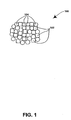
- tuned sealing material 100 are tuned to absorb electromagnetic radiation of a selected frequency.
- light e.g. laser light
- the tuned component of tuned sealing material 100 will readily absorb the electromagnetic radiation of the selected frequency.
- the tuned component will expedite the heating and subsequent melting of tuned sealing material 100.
- the present not claimed explanatory example reduces the amount of time during which the sealing material must be subjected to the laser beam.
- the tuned component of tuned sealing material 100 will readily absorb the electromagnetic radiation of the selected frequency (e.g.
- molecule 200 of filler material can also suitably turned to absorb laser light of various other wavelengths, to absorb visible light, to absorb microwave radiation, to absorb infrared radiation, and the like.
- the tuned sealing material is comprised of a plurality of filler materials.
- more than one of the plurality of filler materials can be suitably stained to absorb one or more than one respective selected frequencies of the electromagnetic radiation.
- molecule 300 of glass material is tuned to absorb electromagnetic radiation of a selected frequency by staining molecule 300 of glass material. More particularly, in the present not claimed explanatory example, molecule 300 of glass material has stained regions 302 which were stained with an electromagnetic radiation absorbing material. That is, the material used to stain molecule 300 of glass material is a material which will absorb electromagnetic radiation of a selected frequency.
- the material used to stain molecule 300 of glass material is intended to absorb light from a gallium arsenide laser (i.e.
- the tuned sealing material is comprised of a plurality of glass materials. Additionally, also more than one of the plurality of glass materials can be suitably stained to absorb one or more than one respective selected frequencies of the electromagnetic radiation.
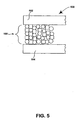
- backplate 502 is stained with material to provide stained regions, typically shown as 602.
- stained regions 602 are stained with an electromagnetic radiation absorbing material. That is, the material used to stain backplate 502 is a material which will absorb electromagnetic radiation of a selected frequency.
- backplate 502 will now more readily absorb selected electromagnetic radiation.
- the present embodiment further expedites, for example, the heating and subsequent melting of the sealing material by providing a heated surface (i.e. the surface of stained backplate 502) which is thermally coupled to tuned sealing material 100.
- the material used to stain backplate 502 and the material used to stain faceplate 504 is chosen so that it will enhance the absorption of electromagnetic radiation having a frequency different from the frequency of the electromagnetic radiation which will be readily absorbed by tuned sealing material 100.
- three separate electromagnetic radiation sources can be used to selectively, for example, heat tuned sealing material 100, backplate 502, or faceplate 504.
- the material used to stain thin film 802 and the material used to stain thin film 804 is chosen so that it will enhance the absorption of electromagnetic radiation having a frequency different from the frequency of the electromagnetic radiation which will be readily absorbed by tuned sealing material 100.
- three separate electromagnetic radiation sources can be used to selectively, for example, heat tuned sealing material 100, thin film 802, or thin film 804.
- the present embodiment specifically recites having thin film coupled to each of backplate 502 and faceplate 504, the present invention is also well suited to an embodiment in which only one of backplate 502 and faceplate 504 have a thin film coupled thereto.
Landscapes
- Chemical & Material Sciences (AREA)
- Engineering & Computer Science (AREA)
- Life Sciences & Earth Sciences (AREA)
- Chemical Kinetics & Catalysis (AREA)
- General Chemical & Material Sciences (AREA)
- Geochemistry & Mineralogy (AREA)
- Materials Engineering (AREA)
- Organic Chemistry (AREA)
- Ceramic Engineering (AREA)
- Joining Of Glass To Other Materials (AREA)
- Glass Compositions (AREA)
- Manufacture Of Electron Tubes, Discharge Lamp Vessels, Lead-In Wires, And The Like (AREA)
- Vessels, Lead-In Wires, Accessory Apparatuses For Cathode-Ray Tubes (AREA)
- Cathode-Ray Tubes And Fluorescent Screens For Display (AREA)
- Adhesives Or Adhesive Processes (AREA)
- Shielding Devices Or Components To Electric Or Magnetic Fields (AREA)
- Laminated Bodies (AREA)
Claims (8)
- Verfahren zum Befestigen einer ersten Fläche an eine zweite Fläche, wobei die erste und die zweite Fläche zu einer Rückplatte und einer Frontplatte einer Flachpanelanzeigeeinrichtung gehören, und das Verfahren die Schritte aufweist:a) Anbringen eines eingestellten Dichtungsmaterials (100) zwischen der ersten Fläche (502) und der zweiten Fläche (504), wobei das eingestellte Dichtungsmaterial ein Füllmaterial (102; 200) als eine erste Komponente und ein Glasmaterial (104; 300) als eine zweite Komponente aufweist, die mit dem Füllmaterial gemischt ist, wobei zumindest eine Komponente eingestellt ist, um eine elektromagnetische Strahlung einer ausgewählten Frequenz von Mikrowellenstrahlung, Infrarotstrahlung, sichtbarem Licht oder ultraviolettem Licht zu absorbieren;b) Aussetzen des eingestellten Dichtmaterials (100) einer elektromagnetischen Strahlung der ausgewählten Frequenz, so dass das eingestellte Dichtmaterial (100) die elektromagnetische Strahlung der ausgewählten Frequenz absorbiert, und Aussetzen der ersten Fläche (502) einer elektromagnetischen Strahlung einer zweiten ausgewählten Frequenz einer Mikrowellenstrahlung, Infrarotstrahlung, sichtbarem Licht oder ultraviolettem Licht, die verschieden von der ausgewählten Frequenz ist, wobei die erste Fläche (502) Bereiche (602) aufweist, die die elektromagnetische Frequenz absorbieren, so dass die erste Fläche (502) die elektromagnetische Strahlung der zweiten ausgewählten Frequenz absorbiert; undc) Verwenden des eingestellten Dichtmaterials (100), das der elektromagnetischen Strahlung der ausgewählten Frequenz ausgesetzt wurde, um die erste Fläche (502) und die zweite Fläche (504) aneinander zu befestigen.
- Verfahren zum Befestigen einer ersten Fläche an eine zweite Fläche nach Anspruch 1, wobei Schritt b) ferner den Schritt aufweist:Aussetzen der ersten Fläche (502) und der zweiten Fläche (504) einer elektromagnetischen Strahlung der zweiten ausgewählten Frequenz, wobei die erste Fläche (502) und die zweite Fläche (504) jeweils Bereiche (602) aufweisen, die die elektromagnetische Frequenz absorbieren, so dass die erste Fläche (502) und die zweite Fläche (504) die elektromagnetische Strahlung der zweiten ausgewählten Frequenz absorbieren.
- Verfahren zum Befestigen einer ersten Fläche an eine zweite Fläche, wobei die erste und die zweite Fläche zu einer Rückplatte und einer Frontplatte einer Flachpanelanzeigeeinrichtung gehören, und wobei das Verfahren die Schritte aufweist:Anbringen einer dünnen Schicht (802; 804) auf die erste Fläche (502) und/oder die zweite Fläche (504), wobei die dünne Schicht (802; 804) angepasst ist, um eine elektromagnetische Strahlung einer ausgewählten Frequenz zu absorbieren;Anbringen eines eingestellten Dichtmaterials (100) zwischen der ersten Fläche (502) und der zweiten Fläche (504), wobei das eingestellte Dichtmaterial ein Füllmaterial (102; 200) als eine erste Komponente und ein Glasmaterial (104; 300) als eine zweite Komponente aufweist, die mit dem Füllmaterial gemischt ist, wobei zumindest eine Komponente eingestellt ist, um eine elektromagnetische Strahlung einer zweiten ausgewählten Frequenz einer Mikrowellenstrahlung, einer Infrarotstrahlung, sichtbarem Licht oder ultraviolettem Licht zu absorbieren, die verschieden von der ausgewählten Frequenz ist;Aussetzen des eingestellten Dichtmaterials (100) einer elektromagnetischen Strahlung der zweiten ausgewählten Frequenz, so dass das eingestellte Dichtmaterial (100) die elektromagnetische Strahlung der zweiten ausgewählten Frequenz absorbiert;Aussetzen der dünnen Schicht (802; 804) einer elektromagnetischen Strahlung der ausgewählten Frequenz, so dass die dünne Schicht (802; 804) die elektromagnetische Strahlung der ausgewählten Frequenz absorbiert; undVerwenden des eingestellten Dichtmaterials (100), das der elektromagnetischen Strahlung der zweiten ausgewählten Frequenz ausgesetzt wurde, um die erste Fläche (502) und die zweite Fläche (504) aneinander zu befestigen.
- Verfahren zum Befestigen einer ersten Fläche an eine zweite Fläche nach Anspruch 1 oder Anspruch 3, wobei die erste Komponente (102) eine Vielzahl von Füllmaterialien aufweist.
- Verfahren zum Befestigen einer ersten Fläche an eine zweite Fläche nach Anspruch 1 oder Anspruch 3, wobei die zweite Komponente (104) eine Vielzahl von Glasmaterialien aufweist.
- Verfahren zum Befestigen einer ersten Fläche an eine zweite Fläche nach Anspruch 1 oder Anspruch 3, wobei eine elektromagnetische Strahlung absorbierendes Material (202; 302) aus der Gruppe, die aus Kupferoxiden, Eisenoxiden, Chromoxiden und Eisenchromaten besteht, ausgewählt ist.
- Verfahren zum Befestigen einer ersten Fläche an eine zweite Fläche nach Anspruch 1 oder Anspruch 3, wobei die erste Fläche (502) eine Rückplatte (502) einer Feldemissionsanzeigeeinrichtung ist.
- Verfahren zum Befestigen einer ersten Fläche an eine zweite Fläche nach Anspruch 1 oder 3, wobei die zweite Fläche (504) eine Frontplatte einer Feldemissionsanzeigeeinrichtung ist.
Applications Claiming Priority (3)
| Application Number | Priority Date | Filing Date | Title |
|---|---|---|---|
| US495404 | 2000-01-31 | ||
| US09/495,404 US6555025B1 (en) | 2000-01-31 | 2000-01-31 | Tuned sealing material for sealing of a flat panel display |
| PCT/US2001/000819 WO2001055042A1 (en) | 2000-01-31 | 2001-01-08 | Tuned sealing material and sealing method |
Publications (2)
| Publication Number | Publication Date |
|---|---|
| EP1255705A1 EP1255705A1 (de) | 2002-11-13 |
| EP1255705B1 true EP1255705B1 (de) | 2011-07-06 |
Family
ID=23968526
Family Applications (1)
| Application Number | Title | Priority Date | Filing Date |
|---|---|---|---|
| EP01946834A Expired - Lifetime EP1255705B1 (de) | 2000-01-31 | 2001-01-08 | Abgestimmtes versiegelungswerkstoff und versiegelungsverfahren |
Country Status (7)
| Country | Link |
|---|---|
| US (1) | US6555025B1 (de) |
| EP (1) | EP1255705B1 (de) |
| JP (1) | JP4865179B2 (de) |
| AU (1) | AU2001229344A1 (de) |
| MY (1) | MY126923A (de) |
| TW (1) | TWI264424B (de) |
| WO (1) | WO2001055042A1 (de) |
Families Citing this family (69)
| Publication number | Priority date | Publication date | Assignee | Title |
|---|---|---|---|---|
| US6998776B2 (en) * | 2003-04-16 | 2006-02-14 | Corning Incorporated | Glass package that is hermetically sealed with a frit and method of fabrication |
| US7344901B2 (en) * | 2003-04-16 | 2008-03-18 | Corning Incorporated | Hermetically sealed package and method of fabricating of a hermetically sealed package |
| KR100645533B1 (ko) * | 2005-05-27 | 2006-11-14 | 삼성에스디아이 주식회사 | 유기전계발광표시소자 및 그의 제조 방법 |
| KR100685845B1 (ko) * | 2005-10-21 | 2007-02-22 | 삼성에스디아이 주식회사 | 유기전계 발광표시장치 및 그 제조방법 |
| JP2007184279A (ja) | 2005-12-30 | 2007-07-19 | Samsung Sdi Co Ltd | 有機発光素子およびその製造方法 |
| US8038495B2 (en) * | 2006-01-20 | 2011-10-18 | Samsung Mobile Display Co., Ltd. | Organic light-emitting display device and manufacturing method of the same |
| KR100673765B1 (ko) * | 2006-01-20 | 2007-01-24 | 삼성에스디아이 주식회사 | 유기전계발광 표시장치 및 그 제조방법 |
| US20070170846A1 (en) * | 2006-01-23 | 2007-07-26 | Choi Dong-Soo | Organic light emitting display and method of fabricating the same |
| KR100635514B1 (ko) * | 2006-01-23 | 2006-10-18 | 삼성에스디아이 주식회사 | 유기전계발광표시장치 및 그 제조방법 |
| JP4456092B2 (ja) * | 2006-01-24 | 2010-04-28 | 三星モバイルディスプレイ株式會社 | 有機電界発光表示装置及びその製造方法 |
| JP4624309B2 (ja) * | 2006-01-24 | 2011-02-02 | 三星モバイルディスプレイ株式會社 | 有機電界発光表示装置及びその製造方法 |
| US7999372B2 (en) * | 2006-01-25 | 2011-08-16 | Samsung Mobile Display Co., Ltd. | Organic light emitting display device and method of fabricating the same |
| KR100671641B1 (ko) * | 2006-01-25 | 2007-01-19 | 삼성에스디아이 주식회사 | 유기 전계 발광 표시장치 및 그 제조 방법 |
| KR100685853B1 (ko) * | 2006-01-25 | 2007-02-22 | 삼성에스디아이 주식회사 | 유기전계발광표시장치 및 그 제조방법 |
| KR100671646B1 (ko) | 2006-01-25 | 2007-01-19 | 삼성에스디아이 주식회사 | 유기 전계 발광 표시장치 및 그 제조 방법 |
| KR100685854B1 (ko) | 2006-01-25 | 2007-02-22 | 삼성에스디아이 주식회사 | 유기전계발광표시장치 및 그 제조방법 |
| KR100688795B1 (ko) * | 2006-01-25 | 2007-03-02 | 삼성에스디아이 주식회사 | 유기전계발광 표시장치 및 그 제조방법 |
| KR100688796B1 (ko) * | 2006-01-25 | 2007-03-02 | 삼성에스디아이 주식회사 | 유기전계발광 표시 장치 및 그의 제작 방법 |
| US8164257B2 (en) * | 2006-01-25 | 2012-04-24 | Samsung Mobile Display Co., Ltd. | Organic light emitting display and method of fabricating the same |
| KR100671647B1 (ko) * | 2006-01-26 | 2007-01-19 | 삼성에스디아이 주식회사 | 유기전계발광 표시 장치 |
| JP4633674B2 (ja) * | 2006-01-26 | 2011-02-16 | 三星モバイルディスプレイ株式會社 | 有機電界発光表示装置及びその製造方法 |
| KR100732808B1 (ko) * | 2006-01-26 | 2007-06-27 | 삼성에스디아이 주식회사 | 유기전계발광 표시장치의 제조방법 |
| KR100703472B1 (ko) * | 2006-01-26 | 2007-04-03 | 삼성에스디아이 주식회사 | 프릿 경화 장치 및 이를 이용한 경화 방법 |
| JP4555258B2 (ja) * | 2006-01-26 | 2010-09-29 | 三星モバイルディスプレイ株式會社 | 有機電界発光表示装置 |
| KR100688789B1 (ko) * | 2006-01-27 | 2007-03-02 | 삼성에스디아이 주식회사 | 유기전계발광 표시 장치 및 그의 제조 방법 |
| KR100688790B1 (ko) * | 2006-01-27 | 2007-03-02 | 삼성에스디아이 주식회사 | 유기 전계 발광 표시장치 및 그 제조 방법 |
| KR100688792B1 (ko) * | 2006-01-27 | 2007-03-02 | 삼성에스디아이 주식회사 | 평판 표시장치 및 그의 제조방법 |
| KR100671639B1 (ko) * | 2006-01-27 | 2007-01-19 | 삼성에스디아이 주식회사 | 유기 전계 발광 표시장치 및 그 제조 방법 |
| KR100711882B1 (ko) * | 2006-01-27 | 2007-04-25 | 삼성에스디아이 주식회사 | 유기 전계 발광표시장치 및 그의 제조방법 |
| KR100759666B1 (ko) * | 2006-01-27 | 2007-09-17 | 삼성에스디아이 주식회사 | 평판 표시장치 및 그의 제조방법 |
| KR100759667B1 (ko) * | 2006-01-27 | 2007-09-17 | 삼성에스디아이 주식회사 | 평판 표시장치 및 그의 제조방법 |
| KR100645706B1 (ko) * | 2006-01-27 | 2006-11-15 | 삼성에스디아이 주식회사 | 유기전계발광 표시장치 및 그 제조방법 |
| KR100688791B1 (ko) | 2006-01-27 | 2007-03-02 | 삼성에스디아이 주식회사 | 유기 전계 발광 표시장치 및 그 제조 방법. |
| KR100671643B1 (ko) * | 2006-01-27 | 2007-01-19 | 삼성에스디아이 주식회사 | 유기전계발광 표시 장치 및 그의 제조 방법 |
| JP2007220647A (ja) * | 2006-02-14 | 2007-08-30 | Samsung Sdi Co Ltd | 有機電界発光表示装置及びその製造方法 |
| JP2007220648A (ja) * | 2006-02-14 | 2007-08-30 | Samsung Sdi Co Ltd | 平板表示装置とその製造装置及び製造方法 |
| US7564185B2 (en) * | 2006-02-20 | 2009-07-21 | Samsung Mobile Display Co., Ltd. | Organic electroluminescence display device and manufacturing method thereof |
| KR100713987B1 (ko) * | 2006-02-20 | 2007-05-04 | 삼성에스디아이 주식회사 | 기판 밀착장치 및 이를 이용한 유기전계발광 표시장치의밀봉방법 |
| KR100703446B1 (ko) * | 2006-02-21 | 2007-04-03 | 삼성에스디아이 주식회사 | 유기 전계 발광표시장치의 제조방법 |
| KR100703519B1 (ko) * | 2006-02-21 | 2007-04-03 | 삼성에스디아이 주식회사 | 유기 전계 발광표시장치의 제조방법 |
| JP2007242591A (ja) * | 2006-03-08 | 2007-09-20 | Samsung Sdi Co Ltd | 有機電界発光表示装置及びその製造方法 |
| KR100732817B1 (ko) * | 2006-03-29 | 2007-06-27 | 삼성에스디아이 주식회사 | 유기전계발광 표시장치 및 그 제조방법 |
| KR100703457B1 (ko) * | 2006-04-07 | 2007-04-03 | 삼성에스디아이 주식회사 | 유기 전계 발광 표시장치 및 그 제조 방법 |
| KR100703458B1 (ko) * | 2006-04-20 | 2007-04-03 | 삼성에스디아이 주식회사 | 유기전계발광 표시 장치 및 그의 제작 방법 |
| KR100722119B1 (ko) * | 2006-09-20 | 2007-05-25 | 삼성에스디아이 주식회사 | 유기전계발광 표시 장치 |
| KR100769425B1 (ko) * | 2006-09-21 | 2007-10-22 | 삼성에스디아이 주식회사 | 유기전계발광 표시장치 |
| KR100729084B1 (ko) * | 2006-09-21 | 2007-06-14 | 삼성에스디아이 주식회사 | 유기 전계 발광표시장치 |
| KR20080051756A (ko) * | 2006-12-06 | 2008-06-11 | 삼성에스디아이 주식회사 | 유기 발광 표시 장치 및 그 제조 방법 |
| KR100787463B1 (ko) * | 2007-01-05 | 2007-12-26 | 삼성에스디아이 주식회사 | 글래스 프릿, 실링재 형성용 조성물, 발광 장치 및 발광 장치의 제조방법 |
| JP5440997B2 (ja) * | 2008-08-21 | 2014-03-12 | 日本電気硝子株式会社 | 有機elディスプレイ用封着材料 |
| JP5552743B2 (ja) * | 2008-03-28 | 2014-07-16 | 旭硝子株式会社 | フリット |
| US8440479B2 (en) * | 2009-05-28 | 2013-05-14 | Corning Incorporated | Method for forming an organic light emitting diode device |
| US8072056B2 (en) | 2009-06-10 | 2011-12-06 | Medtronic, Inc. | Apparatus for restricting moisture ingress |
| JP2011060697A (ja) * | 2009-09-14 | 2011-03-24 | Canon Inc | 画像表示装置の製造方法 |
| US8666505B2 (en) | 2010-10-26 | 2014-03-04 | Medtronic, Inc. | Wafer-scale package including power source |
| US9171721B2 (en) | 2010-10-26 | 2015-10-27 | Medtronic, Inc. | Laser assisted direct bonding |
| US8796109B2 (en) | 2010-12-23 | 2014-08-05 | Medtronic, Inc. | Techniques for bonding substrates using an intermediate layer |
| US8424388B2 (en) | 2011-01-28 | 2013-04-23 | Medtronic, Inc. | Implantable capacitive pressure sensor apparatus and methods regarding same |
| EP2751044B1 (de) * | 2011-09-13 | 2020-04-22 | Ferro Corporation | Induktionsversiegelung von anorganischen substraten |
| DK2773596T3 (da) * | 2011-11-02 | 2020-09-14 | Ferro Corp | Mikrobølgeforsegling af uorganiske substrater ved anvendelse af lavsmeltende glassystemer |
| US9362522B2 (en) * | 2012-10-26 | 2016-06-07 | Semiconductor Energy Laboratory Co., Ltd. | Method for bonding substrates, method for manufacturing sealing structure, and method for manufacturing light-emitting device |
| KR102160829B1 (ko) | 2012-11-02 | 2020-09-28 | 가부시키가이샤 한도오따이 에네루기 켄큐쇼 | 밀봉체 및 밀봉체의 제작 방법 |
| US9666763B2 (en) | 2012-11-30 | 2017-05-30 | Corning Incorporated | Glass sealing with transparent materials having transient absorption properties |
| CN107406292B (zh) | 2014-10-31 | 2021-03-16 | 康宁股份有限公司 | 激光焊接的玻璃封装和制造方法 |
| US10136535B2 (en) | 2014-12-24 | 2018-11-20 | Medtronic, Inc. | Hermetically-sealed packages including feedthrough assemblies |
| US9865533B2 (en) | 2014-12-24 | 2018-01-09 | Medtronic, Inc. | Feedthrough assemblies |
| US10124559B2 (en) | 2014-12-24 | 2018-11-13 | Medtronic, Inc. | Kinetically limited nano-scale diffusion bond structures and methods |
| US9968794B2 (en) | 2014-12-24 | 2018-05-15 | Medtronic, Inc. | Implantable medical device system including feedthrough assembly and method of forming same |
| US10098589B2 (en) | 2015-12-21 | 2018-10-16 | Medtronic, Inc. | Sealed package and method of forming same |
Family Cites Families (11)
| Publication number | Priority date | Publication date | Assignee | Title |
|---|---|---|---|---|
| JPS5241156B2 (de) | 1973-08-20 | 1977-10-17 | ||
| US4238704A (en) | 1979-02-12 | 1980-12-09 | Corning Glass Works | Sealed beam lamp of borosilicate glass with a sealing glass of zinc silicoborate and a mill addition of cordierite |
| US4441051A (en) * | 1982-02-22 | 1984-04-03 | General Electric Company | Lamp seal glass |
| JPH02263732A (ja) | 1989-04-05 | 1990-10-26 | Alps Electric Co Ltd | 磁気ヘッド用吸光融着性ガラス |
| US5424605A (en) | 1992-04-10 | 1995-06-13 | Silicon Video Corporation | Self supporting flat video display |
| US5366664A (en) * | 1992-05-04 | 1994-11-22 | The Penn State Research Foundation | Electromagnetic shielding materials |
| US5545474A (en) * | 1994-03-01 | 1996-08-13 | Martin Marietta Corporation | Electromagnetic-attenuating coating materials |
| JP3405067B2 (ja) * | 1995-07-20 | 2003-05-12 | 東陶機器株式会社 | 放電灯の加熱処理装置及び放電灯の封止装置及び その封止方法 |
| JPH0986959A (ja) | 1995-07-20 | 1997-03-31 | Toto Ltd | 赤外線加熱溶融用封着ガラス |
| US5958303A (en) * | 1996-11-07 | 1999-09-28 | Carmel Olefins Ltd | Electrically conductive compositions and methods for producing same |
| US5820435A (en) | 1996-12-12 | 1998-10-13 | Candescent Technologies Corporation | Gap jumping to seal structure including tacking of structure |
-
2000
- 2000-01-31 US US09/495,404 patent/US6555025B1/en not_active Expired - Fee Related
-
2001
- 2001-01-08 WO PCT/US2001/000819 patent/WO2001055042A1/en not_active Ceased
- 2001-01-08 EP EP01946834A patent/EP1255705B1/de not_active Expired - Lifetime
- 2001-01-08 AU AU2001229344A patent/AU2001229344A1/en not_active Abandoned
- 2001-01-08 JP JP2001554991A patent/JP4865179B2/ja not_active Expired - Fee Related
- 2001-01-22 MY MYPI20010290A patent/MY126923A/en unknown
- 2001-06-22 TW TW090100831A patent/TWI264424B/zh not_active IP Right Cessation
Also Published As
| Publication number | Publication date |
|---|---|
| JP2003522089A (ja) | 2003-07-22 |
| US6555025B1 (en) | 2003-04-29 |
| TWI264424B (en) | 2006-10-21 |
| MY126923A (en) | 2006-10-31 |
| EP1255705A1 (de) | 2002-11-13 |
| JP4865179B2 (ja) | 2012-02-01 |
| WO2001055042A1 (en) | 2001-08-02 |
| AU2001229344A1 (en) | 2001-08-07 |
Similar Documents
| Publication | Publication Date | Title |
|---|---|---|
| US6555025B1 (en) | Tuned sealing material for sealing of a flat panel display | |
| US6129603A (en) | Low temperature glass frit sealing for thin computer displays | |
| JP2754461B2 (ja) | 容器の封着方法および封着装置 | |
| US4069567A (en) | Method of installing a color selection electrode in a color cathode ray tube | |
| US6109994A (en) | Gap jumping to seal structure, typically using combination of vacuum and non-vacuum environments | |
| US20070001579A1 (en) | Glass-to-glass joining method using laser, vacuum envelope manufactured by the method, electron emission display having the vacuum envelope | |
| WO1999056301A1 (en) | Microwave sealing of flat panel displays | |
| JP3270054B2 (ja) | 蛍光体画素を対応電界エミッタに整列させる内部構造を有する電界放出装置 | |
| US8475618B2 (en) | Manufacturing method of hermetic container | |
| US5820435A (en) | Gap jumping to seal structure including tacking of structure | |
| KR20020020188A (ko) | 밀봉용기, 그 제조방법 및 이러한 밀봉용기를 이용하는표시장치 | |
| EP0944912B1 (de) | Spaltsprungverfahren zur abdichtung von plattenstrukturen | |
| US5785569A (en) | Method for manufacturing hollow spacers | |
| KR100845732B1 (ko) | 동조 실링재 및 실링방법 | |
| US6827621B1 (en) | Method and apparatus for manufacturing flat image display device | |
| US6533632B1 (en) | Method of evacuating and sealing flat panel displays and flat panel displays using same | |
| US5167687A (en) | Method for laminating and bonding flat electrodes | |
| KR100447130B1 (ko) | 전계 방출 표시소자의 캡 실링방법 및 그의 제조방법 | |
| US7067789B2 (en) | Method and device for producing X-ray image detector, and X-ray image detector | |
| US7714496B2 (en) | Field emission display device and field emission type backlight device having a sealing structure for vacuum exhaust | |
| KR20120031892A (ko) | 내부가 감압된 분위기를 유지하는 기밀 용기의 제조 방법 | |
| JP3248041B2 (ja) | 画像形成装置及びその製造方法 | |
| JP3940583B2 (ja) | 平面表示装置およびその製造方法 | |
| JP2005251475A (ja) | 画像表示装置 | |
| EP1059655A2 (de) | Vorrichtung zur Aufrechthalung des Heliumdrucks in den Kanälen einer Palc-Anzeigetafel |
Legal Events
| Date | Code | Title | Description |
|---|---|---|---|
| PUAI | Public reference made under article 153(3) epc to a published international application that has entered the european phase |
Free format text: ORIGINAL CODE: 0009012 |
|
| 17P | Request for examination filed |
Effective date: 20020826 |
|
| AK | Designated contracting states |
Kind code of ref document: A1 Designated state(s): AT BE CH CY DE DK ES FI FR GB GR IE IT LI LU MC NL PT SE TR |
|
| AX | Request for extension of the european patent |
Free format text: AL;LT;LV;MK;RO;SI |
|
| RBV | Designated contracting states (corrected) |
Designated state(s): DE FR GB IE NL |
|
| 17Q | First examination report despatched |
Effective date: 20050202 |
|
| RAP1 | Party data changed (applicant data changed or rights of an application transferred) |
Owner name: CANON KABUSHIKI KAISHA |
|
| GRAP | Despatch of communication of intention to grant a patent |
Free format text: ORIGINAL CODE: EPIDOSNIGR1 |
|
| GRAS | Grant fee paid |
Free format text: ORIGINAL CODE: EPIDOSNIGR3 |
|
| GRAA | (expected) grant |
Free format text: ORIGINAL CODE: 0009210 |
|
| AK | Designated contracting states |
Kind code of ref document: B1 Designated state(s): DE FR GB IE NL |
|
| REG | Reference to a national code |
Ref country code: GB Ref legal event code: FG4D |
|
| REG | Reference to a national code |
Ref country code: IE Ref legal event code: FG4D |
|
| REG | Reference to a national code |
Ref country code: DE Ref legal event code: R096 Ref document number: 60144916 Country of ref document: DE Effective date: 20110825 |
|
| REG | Reference to a national code |
Ref country code: HK Ref legal event code: WD Ref document number: 1051029 Country of ref document: HK |
|
| REG | Reference to a national code |
Ref country code: NL Ref legal event code: T3 |
|
| PLBE | No opposition filed within time limit |
Free format text: ORIGINAL CODE: 0009261 |
|
| STAA | Information on the status of an ep patent application or granted ep patent |
Free format text: STATUS: NO OPPOSITION FILED WITHIN TIME LIMIT |
|
| 26N | No opposition filed |
Effective date: 20120411 |
|
| REG | Reference to a national code |
Ref country code: DE Ref legal event code: R097 Ref document number: 60144916 Country of ref document: DE Effective date: 20120411 |
|
| PGFP | Annual fee paid to national office [announced via postgrant information from national office to epo] |
Ref country code: IE Payment date: 20121212 Year of fee payment: 13 |
|
| PGFP | Annual fee paid to national office [announced via postgrant information from national office to epo] |
Ref country code: FR Payment date: 20130214 Year of fee payment: 13 Ref country code: DE Payment date: 20130131 Year of fee payment: 13 Ref country code: GB Payment date: 20130123 Year of fee payment: 13 |
|
| PGFP | Annual fee paid to national office [announced via postgrant information from national office to epo] |
Ref country code: NL Payment date: 20130131 Year of fee payment: 13 |
|
| REG | Reference to a national code |
Ref country code: DE Ref legal event code: R119 Ref document number: 60144916 Country of ref document: DE |
|
| REG | Reference to a national code |
Ref country code: NL Ref legal event code: V1 Effective date: 20140801 |
|
| GBPC | Gb: european patent ceased through non-payment of renewal fee |
Effective date: 20140108 |
|
| REG | Reference to a national code |
Ref country code: DE Ref legal event code: R119 Ref document number: 60144916 Country of ref document: DE Effective date: 20140801 |
|
| PG25 | Lapsed in a contracting state [announced via postgrant information from national office to epo] |
Ref country code: NL Free format text: LAPSE BECAUSE OF NON-PAYMENT OF DUE FEES Effective date: 20140801 Ref country code: DE Free format text: LAPSE BECAUSE OF NON-PAYMENT OF DUE FEES Effective date: 20140801 |
|
| REG | Reference to a national code |
Ref country code: FR Ref legal event code: ST Effective date: 20140930 |
|
| REG | Reference to a national code |
Ref country code: IE Ref legal event code: MM4A |
|
| PG25 | Lapsed in a contracting state [announced via postgrant information from national office to epo] |
Ref country code: GB Free format text: LAPSE BECAUSE OF NON-PAYMENT OF DUE FEES Effective date: 20140108 Ref country code: FR Free format text: LAPSE BECAUSE OF NON-PAYMENT OF DUE FEES Effective date: 20140131 |
|
| PG25 | Lapsed in a contracting state [announced via postgrant information from national office to epo] |
Ref country code: IE Free format text: LAPSE BECAUSE OF NON-PAYMENT OF DUE FEES Effective date: 20140108 |