EP1237160A2 - Leseverstärkersteuerschaltung für Halbleiterspeicheranordnung - Google Patents
Leseverstärkersteuerschaltung für Halbleiterspeicheranordnung Download PDFInfo
- Publication number
- EP1237160A2 EP1237160A2 EP01131050A EP01131050A EP1237160A2 EP 1237160 A2 EP1237160 A2 EP 1237160A2 EP 01131050 A EP01131050 A EP 01131050A EP 01131050 A EP01131050 A EP 01131050A EP 1237160 A2 EP1237160 A2 EP 1237160A2
- Authority
- EP
- European Patent Office
- Prior art keywords
- sense amplifier
- transistors
- control circuit
- memory device
- semiconductor memory
- Prior art date
- Legal status (The legal status is an assumption and is not a legal conclusion. Google has not performed a legal analysis and makes no representation as to the accuracy of the status listed.)
- Withdrawn
Links
Images
Classifications
-
- G—PHYSICS
- G11—INFORMATION STORAGE
- G11C—STATIC STORES
- G11C7/00—Arrangements for writing information into, or reading information out from, a digital store
- G11C7/06—Sense amplifiers; Associated circuits, e.g. timing or triggering circuits
- G11C7/08—Control thereof
-
- G—PHYSICS
- G11—INFORMATION STORAGE
- G11C—STATIC STORES
- G11C7/00—Arrangements for writing information into, or reading information out from, a digital store
- G11C7/06—Sense amplifiers; Associated circuits, e.g. timing or triggering circuits
- G11C7/065—Differential amplifiers of latching type
-
- G—PHYSICS
- G11—INFORMATION STORAGE
- G11C—STATIC STORES
- G11C11/00—Digital stores characterised by the use of particular electric or magnetic storage elements; Storage elements therefor
- G11C11/21—Digital stores characterised by the use of particular electric or magnetic storage elements; Storage elements therefor using electric elements
- G11C11/34—Digital stores characterised by the use of particular electric or magnetic storage elements; Storage elements therefor using electric elements using semiconductor devices
- G11C11/40—Digital stores characterised by the use of particular electric or magnetic storage elements; Storage elements therefor using electric elements using semiconductor devices using transistors
- G11C11/401—Digital stores characterised by the use of particular electric or magnetic storage elements; Storage elements therefor using electric elements using semiconductor devices using transistors forming cells needing refreshing or charge regeneration, i.e. dynamic cells
- G11C11/4063—Auxiliary circuits, e.g. for addressing, decoding, driving, writing, sensing or timing
- G11C11/407—Auxiliary circuits, e.g. for addressing, decoding, driving, writing, sensing or timing for memory cells of the field-effect type
- G11C11/409—Read-write [R-W] circuits
- G11C11/4091—Sense or sense/refresh amplifiers, or associated sense circuitry, e.g. for coupled bit-line precharging, equalising or isolating
-
- H—ELECTRICITY
- H10—SEMICONDUCTOR DEVICES; ELECTRIC SOLID-STATE DEVICES NOT OTHERWISE PROVIDED FOR
- H10B—ELECTRONIC MEMORY DEVICES
- H10B12/00—Dynamic random access memory [DRAM] devices
- H10B12/50—Peripheral circuit region structures
-
- G—PHYSICS
- G11—INFORMATION STORAGE
- G11C—STATIC STORES
- G11C2207/00—Indexing scheme relating to arrangements for writing information into, or reading information out from, a digital store
- G11C2207/06—Sense amplifier related aspects
- G11C2207/065—Sense amplifier drivers
Definitions
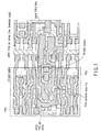
- Some conventional semiconductor memory devices use a sense amplifier consisting of a latch type differential amplifier circuit.
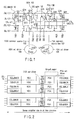
- the circuit arrangement of a conventional differential amplifier will be described below in terms of a sense amplifier section for amplifying the bit-line potential in a dynamic random access memory (DRAM) as an example.
- DRAM dynamic random access memory
- the sense amplifier section shown in FIG. 1 includes a bit line pair /BL ⁇ 2> and BL ⁇ 2> ( ⁇ 2> is illustrated by example), an equalizer and multiplexer (EQL&MUX) 101, an N-channel sense amplifier (NSA) 102, an NSA common source line 103, an NSA set driver 104, and a DQ gate 105.
- the equalizer comprises N-channel transistors (hereinafter referred to as NFETs) Q11, Q12, and Q13.
- the multiplexer comprises NFETs Q14 and Q15.
- the NSA 102 comprises NFETs Q16 and Q17.
- the NSA common source line 103 provides a "0" write potential VBLL (e.g., Vss) to the common sources of the NFETs Q16 and Q17 in the NSA 102.
- the NSA set driver 104 provides VBLL to the NSA common source line 103.
- the DQ gate 105 comprises NFETs Q18 and Q19.
- the PSA 106 comprises P-channel transistors (hereinafter referred to as PFETs) Q20 and Q21.
- the PSA common source line 107 transfers a "1" write potential (e.g., VBLH) to the common sources of the transistors Q20 and Q21 in the PSA 106, and the PSA set driver 108 provides VBLH to the PSA common source line 107.
- the PSA 106 is followed by a multiplexer comprised of NFETs Q22 and Q23 and an equalizer comprised of NFETs Q24, Q25 and Q26.
- Such a sense amplifier as described above is provided for each bit line pair; thus, as shown in the lower portion of FIG. 1, the same circuit is also provided for /BL ⁇ 0> and BL ⁇ 0> ( ⁇ 0> is merely exemplary).
- the VBLH/2 power supply lines on the right and left supply the equalized potential VBLH/2 to the bit line pairs.
- CSL denotes a column select signal line.
- memory cells each consisting of a cell capacitor and a cell transistor, are connected on the opposite sides of the sense amplifier section to each bit line pair.
- the major part of the sense amplifier of FIG. 1 is formed from the NSA 102 and PSA 106 each of which has its transistors cross-coupled to the bit line pair.
- the common source line 103 of the NSA 102 is connected by the NSA set driver 104 consisting of an NFET to a bit line restore power supply line at the "0" write potential VBLL (e.g., Vss).
- the common source line 107 of the PSA 106 is connected by the PSA set driver 108 consisting of a PFET to a bit line restore power supply line at the "1" write potential VBLH.
- the NSA set driver is formed of an NFET and the PSA set driver is formed of a PFET.
- latch signals NSET and bPSET are set high and low, respectively, thereby amplifying a small potential difference between the bit lines to set the bit line BL (or the /BL) at "1" write potential on the high potential side and the bit line /BL (or the BL) at "0" write potential on the low potential side, respectively.
- a sense amplifier control circuit for use in a semiconductor memory device comprising: a sense amplifier comprising first transistors of a first conductivity type connected in the form of a latch type differential amplifier; a set driver corresponding to the sense amplifier; and the set driver comprising a second transistor of a second conductivity type for connecting the common source line of the latch type differential amplifier to a restore power supply line.
- one set driver is provided for a relatively small number (for example one to four) of sense amplifiers and the set drivers are placed adjacent to the NSA and PSA at regular intervals in the direction in which the sense amplifier layout is repeated.
- the set drivers thus placed are called the distributed set drivers.
- one NSA set driver is placed every two NSAs and one PSA set driver is placed every two PSAs.
- One set driver is shared among the common source lines of a relatively large number of sense amplifiers and such set drivers are placed together in an area other than the area where the sense amplifiers are laid out repeatedly.
- the set drivers thus placed are called the concentrated set drivers.
- the set drivers may be placed either in the distributed or concentrated form.
- the entire cell array of a DRAM is constructed from many cell array blocks divided by sense amplifier regions. Therefore, a slight increase in the size of each sense amplifier has a great effect on the chip size. For this reason, the concentrated set drivers are generally used in conventional DRAMs.
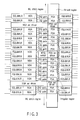
- the concentrated set drivers are frequently placed in WL stitch regions each of which is provided every two or more rows (two or more bit line pairs) in the direction in which word lines (WL) extends (the vertical direction of FIG. 2).
- the WL stitch regions are ones where metal word lines of low resistance and gate interconnect lines of relatively high resistance are stitched.
- the set drivers can be placed in irregular regions resulting from making the repetition period (pitch) of sense amplifiers a little smaller than that of bit line pairs /BL and BL (see USP 5,636,158). An example of such placement is illustrated in FIG. 3.
- the NSA set drivers are placed in WL stitch regions
- the PSA set drivers are placed in the WL stitch regions and the irregular regions including MDQ switches.
- the NFETs are used in far greater numbers than the PFETs.
- the PFETs for the PSAs and PSA set drivers are formed in an N-well region of relatively small width which extends in the direction in which the sense amplifiers are repeated as shown in FIG. 3.
- the reason why the NSA set drivers are placed only in the WL stitch regions is that the P-well regions in the WL stitch regions are large enough to accommodate the NSA set drivers of required size.
- the reason why the PSA set drivers are placed in both the stitch regions and the irregular regions is that the width of the N-well region which is determined to conform to the layout of PSAs by itself is not so large as to allow the stitch regions to accommodate PSA set drivers of sufficient size.
- the entire cell array of DRAMs and the like is formed from many cell array blocks separated by sense amplifier sections.
- it is very important to reduce the sense amplifier size in the bit line direction. For this reason, efforts have been made to form as small a sense amplifier as possible.
- the NFETs are far greater in number than the PFETs.
- the P-well region is far larger than the N-well region in view of the entire layout of sense amplifiers.
- the PFETs have little freedom in layout comparing with the NFETs.
- the NSA set driver connected to one common source line is formed by an NFET and the PSA set driver connected to the other common source line is formed by a PFET, which, in itself, imposes restrictions on the freedom in layout. As a result, it becomes difficult to shrink the size of sense amplifiers.
- the conventional sense amplifier control circuit for use in a semiconductor memory device is configured such that the set driver for NSA is formed by an NFET and set driver for PSA is formed by a PFET; thus, difficulties are involved in shrinking the size of the entire sense amplifier section including control circuits.
- the following embodiments of the present invention will be described in detail to provide the arrangement of a transistor circuit for sense amplifier set drivers which allows the size of the entire sense amplifier section to be shrunk.
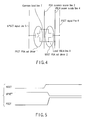
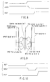
- FIG. 4 shows the arrangement of a transistor circuit for a PSA set driver connected to a PSA common source line of a sense amplifier consisting of latch type differential amplifier circuit.
- the PSA set driver shown in FIG. 4 is composed of a PFET PSA set driver 1, an NFET PSA set driver 2, a PSA common source line 3, a VBLH power supply line 4, a bPSET signal line 5 for activating the PFET PSA set driver, a PSET signal line 6 for activating the NFET PSA set driver, a local common source line 7, and a local VBLH line 8.
- the PSA common line 3 is set at the bit line restore potential VBLH.
- the PSA set drivers connected to the PSA common source line 3 are formed by a PFET and an NFET.
- the P-well region is very large in comparison with the N-well region and hence high in the freedom in layout and placement of the NFET. Therefore, any increase in the layout area accompanied by introducing the NFET PSA set driver 2 can be avoided.
- the formation of the PSA set driver by a PFET and an NFET allows the driving capability conventionally borne by only the PFET PSA set driver to be allocated to the NFET PSA set driver. Therefore, the size of the PFET PSA set driver can be shrunk. In addition, the ratio of allocation can be set arbitrarily; thus, the PSA set driver can be formed by only the NFET PSA set diver 2.
- the layout size of the PFET PSA set driver can also be shrunk simultaneously, allowing the width of the N well to be substantially determined by the layout of the PSA itself.
- the PSA set driver circuit arrangement according to the first embodiment which can be formed by an NFET only or both a PFET and an NFET unlike the conventional sense amplifier control circuit, allows the width of the N well where the PFETs of PSAs are to be placed to be minimized.
- the PSA set driver is formed by a PFET only. The size of the sense amplifier can therefore be shrunk, allowing a semiconductor memory device which is small in chip size and highly competitive in cost to be realized.
- the first embodiment has been described in terms of the circuit arrangement of the PSA set driver, this is not restrictive.
- the NSA set driver is formed from an NFET and a PFET, any increase in the layout area accompanied by introducing the PFET NSA set driver can be avoided.
- the size of the NFET NSA set driver can be shrunk.
- the use of not only an NFET but also a PFET for the NSA set driver provides greater freedom in layout and makes for a reduction in chip size.
- FIG. 5 is a timing diagram for sense amplifier activation signals according to a second embodiment of the present invention.
- the second embodiment is directed to the activation-time potentials of activation signals (set signals) for set drivers which are formed from transistors of opposite conductivity type to transistors in corresponding sense amplifiers.
- the activation signals for set drivers in which the transistors of opposite conductivity type are of N type are set higher than the high supply voltage inside the semiconductor memory device (VINT or VBLH > 0).
- the activation signals for set drivers in which the transistors of opposite conductivity type are of P type are set lower than the low internal supply voltage (Vss, GND, 0V, or VBLL).
- the activation-potential (high level) of the set signal PSET for the NFET PSA set driver (as indicated at 2 in FIG. 4) for PFET PSA is set higher than the internal supply voltage for peripheral circuit, VINT.
- NSET which is the set signal for the NFET NSA set driver for NSA
- the set signal for the PFET PSA set driver for PSA (as indicated at 1 in FIG. 4), bPSET, is set, at activation time, to the low level Vss, GND, or 0V.
- the potential of the set signal PSET at activation time is required to be higher than VBLH by not less than the threshold voltage of the NFET PSA set driver.
- the layout of the set driver can be made small and the size of the sense amplifier can be reduced by increasing the driving capability of the set driver.
- a semiconductor memory device can be realized which is small in chip size and highly competitive in cost.
- the restoring capability of the sense amplifier is increased because of the high driving capability of the set driver, allowing a fast semiconductor memory device to be realized.
- the effect of increasing the driving capability of NFET (or PFET) PSA (or NSA) set driver can be further enhanced by setting the potential of the set signal for activating set driver to an internal boost voltage higher than the external high supply voltage VEXT (VDD) (or lower than the external low supply voltage Vss).
- the third embodiment is directed to setting of the threshold voltage of transistors in set drivers which are of opposite conductivity type to transistors in the corresponding sense amplifiers.
- these transistors are of N type, their threshold voltage is set lower than that of other N-type transistors in the semiconductor memory device; otherwise, the threshold voltage is set higher than that of other P-type transistors.
- the absolute value of the threshold voltage of the transistors of opposite conductivity type is set smaller that that of other transistors of opposite conductivity type in a semiconductor memory device.
- the threshold voltage of NFETs constituting NFET PSA set drivers for P-channel sense amplifiers is set lower that that of other NFETs used in the semiconductor memory device.
- the threshold voltage of other NFETs is usually of the order of 0.5 to 0.6 V.
- the threshold voltage of NFETs constituting NFET PSA set drivers is set to 0.3 V or below (low threshold NFETs).
- low-threshold NFETs are sometimes used as NFETs that constitute N-channel sense amplifiers (NSAs).
- NSAs N-channel sense amplifiers
- the driving capability of the set drivers can be increased, allowing the sense amplifier size to be minimized as in the second embodiment.
- a semiconductor memory device can be realized which is small in chip size and highly competitive in cost.
- the semiconductor memory device provides faster operation because the restoring capability of sense amplifiers is high.
- FIG. 6 shows the arrangement of a fourth embodiment of the present invention.
- set drivers formed by transistors which are of opposite conductivity type to transistors in the corresponding sense amplifiers are placed in either of the previously described word line stitch regions and irregular regions, or in both.
- An example of a layout of such a sense amplifier section is illustrated in FIG. 6.
- the layout of FIG. 6 remains unchanged from the conventional layout in that the EQL&MUX, NSA&DQ gate and PSA are arranged repeatedly as a layout unit, but is characterized in that the repetition period of the layout unit is smaller than that of corresponding bit line pairs.
- Such a layout advantageously increases the area of the irregular region in comparison with the case where the repetition period of only the DQ gate and PSA portion is set smaller as in FIG. 3.
- the repetition period varying region is present in the boundary region between the sense amplifier section and the cell array (not shown) not in the layout of the sense amplifier section provides advantage in layout (refer to the ninth embodiment).
- the NFET PSA set drivers are placed in the word line stitch regions which have been little used heretofore and the newly developed irregular regions in the P well adjoining the N well and having EQL&MUX placed repeatedly. Transistors of required size can be placed without affecting the other layout portion. Therefore, the size of the sense amplifiers can be shrunk to a minimum. As a result, a semiconductor memory device can be realized which is small in chip size and highly competitive in cost. In addition, the semiconductor memory device provides faster operation because the sense amplifiers has high restoring capability.
- FIG. 7 shows the arrangement of a fifth embodiment of the present invention.
- the fifth embodiment is characterized in that the NFET PSA set driver and the PFET PSA set driver are placed adjacent to each other in a word line stitch region or irregular region.
- the region on the left which is indicated by bold broken line is a N well region.
- a PFET PSA set driver indicated by fine broken line, is placed in the center of the N well region. PSAs indicated by fine broken line are repeatedly placed above and below the PSA set driver.
- portions indicated by oblique parallel lines with the right down indicate first metal interconnect lines, whereas portions indicated by oblique parallel lines with the left down indicate gate interconnect lines.
- the pattern layout of FIG. 7 is an enlarged view of the PFET PSA set driver, the PSAs located above and below the set driver, and the NFET PSA set driver immediately to the right of the PFET PSA set driver in the region where the N well region and the irregular region shown in FIG. 6 intersect.
- FIG. 6 the NFET PSA set driver and the PFET PSA set driver are placed adjacent to each other in each of the stitch region and the irregular region.
- FIG. 7 shows a specific example of a layout of the NFET PSA set driver and the PFET PSA set driver which are placed adjacent to each other in the irregular region. The circuit construction of NFET and PFET PSA set drivers in FIG. 7 remain unchanged from those in FIG. 4.
- each of the local VBLH line and the PSA local common source line each of which is formed by a first metal interconnect line, to be shared between them. Therefore, contact with the VBLH power supply line and the PSA common source line (not shown), which are formed above the local interconnect lines by second metal interconnect lines, can be made at any point on the local interconnect lines.
- the VBLH power supply line and the PSA common source line have been formed in the neighborhood of the N well region where the PSAs and the PFET PSA set drivers are arranged.
- the placement of other circuit than the PFET PSA set driver in the stitch or irregular region in the N well adjacent to the NFET PSA set driver in the stitch or irregular region in the P well would make it difficult to connect the VBLH power supply line and the PSA common source line with the local VBLH line and the local PSA common source line, respectively.
- additional second metal interconnect lines might be required to be formed for the NFET PSA set driver.
- the second metal interconnect lines, forming the VBLH line and the PSA common source line need not necessarily be formed in the vicinity of the N well region. That is, they may be formed in the vicinity of the P well region in which the NFET PSA set driver is placed.
- the NFET PSA set driver and the PFET PSA set driver are placed adjacent to each other in the stitch or irregular region, the freedom in layout of the VBLH power supply line and the PSA common source line is increased, allowing the sense amplifier size to be minimized. As a result, a semiconductor memory device can be realized which is small in chip size and highly competitive in cost.
- FIG. 8 is a timing diagram of the set signals in a sixth embodiment of the present invention.
- the sixth embodiment is characterized in that a difference is introduced between times at which the set signals bPSET and PSET activate the PFET and NFET PSA set drivers, respectively, in the sense amplifier set driver of FIG. 4.
- An example of timing of the set signals is illustrated in FIG. 8. As can be seen, a difference in the timing of activation is positively introduced between the set signals bPSET and PSET. The reason is as follows:
- the sense amplifier set driver composed of PFET and NFET PSA set drivers, their driving capability can be controlled during the initial sensing interval and enhanced during the subsequent bit-line potential restoring interval by introducing a time difference between their respective set signals.
- a sense amplifier can be realized which is high in small potential sensing capability and bit-line potential restoring capability.
- the set signal bPSET is enabled to activate the corresponding set driver prior to PSET; however, this order may be reversed.
- the sixth embodiment has been described in terms of the set signals for the PSA set drivers, this is not restrictive.
- a time difference may also be introduced between two set signals bNSET and NSET for activating PFET and NFET NSA set drivers, respectively.
- an NSA can be realized which is high in small potential sensing capability and bit-line potential restoring capability.
- the NSA set driver is composed of two PFETs and the PSA set driver is composed of two NFETs
- a difference in the timing of activation may be introduced between two set signals for activating the two NFETs or PFETs.
- the NSA set driver may further be composed of two sorts of NFETs and PSA set driver, composed of two sorts of PFETs.
- the difference in activation timing may be between two set signals for activating the two sorts of NFETs or PFETs.
- FIGS. 9 and 10 A seventh embodiment of the present invention will be described next with reference to FIGS. 9 and 10.
- the seventh embodiment is described in terms of application of the aforementioned PSA (or NSA) set driver comprising an NFET and a PFET to a common source line overdrive scheme for increasing the operating speed of a semiconductor memory device.
- PSA or NSA
- a VBLHOV power supply line 4a is connected to the PFET PSA set driver 1a to provide an overdrive voltage VBLHOV higher than the final restore voltage VBLH to the PSA common source line 3a at an early stage in the sensing procedure.
- a VBLH power supply line 4 is connected to the NFET PSA set driver 2a to provide the final restore voltage VBLH to the PSA common source line 3.
- FIG. 10 which shows the timing diagram of the set signals
- the set signal bPSET for the PFET PSA set driver 1a connected with the VBLHOV power supply line 4a is first activated to raise rapidly the potential on the PSA common source line 3 toward the final restore voltage VBLH.
- the set signal bPSET is restored to the normal level.
- the set signal PSET for the NFET PSA set driver 2a is activated with the result that the final potential on the PSA common source line 3 reaches the restore voltage VBLH.
- the method is adopted to enhance the driving capability of the NFET PSA set driver 2a by setting the potential of the activated set signal PSET higher than the internal supply voltage VINT in the semiconductor memory device.
- the PFET PSA set driver is connected to the overdrive voltage VBLHOV; instead, the NFET PSA set driver may be connected to VBLHOV.
- the seventh embodiment has been described as overdriving the PSA common source line, in overdriving the NSA common source line, use is made of the overdrive voltage VBLLOV lower than the final restore voltage VBLL. Similar overdriving may also be applied for the case when the NSA set driver is formed of two sorts of PFETs and the PSA set driver, formed of two sorts of NFETs. Furthermore, similar overdriving may be applied for the case when the NSA set driver is formed of two sorts of NFETs and the PSA set driver, formed of two sorts of PFETs.
- the eighth embodiment is characterized in that no contact for biasing the well in which sense amplifier constituent elements are placed is formed within the repetition unit of the sense amplifier layout.
- an N well contact is placed in the PFET PSA set driver formed region in the irregular region resulting from the difference in repetition period between PSAs and bit lines, not in the PSA formed region.
- the width of the N well region comes to be determined by the size of the PSA layout itself.
- the placement of the well contact in the N well in the irregular region reduces the layout region for the PFET PSA set driver by the amount corresponding to that contact. This may make it difficult to place the PFET PSA set driver of the required size.
- an NFET PSA set driver is simply used at the same time as described previously in connection with the first embodiment. It is also possible only to use NFETs for constituting PSA set driver.
- the sense amplifier size can be minimized.
- a semiconductor memory device can be realized which is small in chip size and highly competitive in cost.
- the ninth embodiment is characterized in that, when the repetition period of the sense amplifier layout and the repetition period of the bit line layout differ, the period varying region is present in the boundary region between the sense amplifier section and the cell array as shown in FIG. 6.
- a contact that provides the substrate potential to the well in which sense amplifier circuit elements are formed.
- another contact is placed to provide the bias potential.
- Other circuit elements than these contacts will never be placed in the boundary region between the sense amplifier section and the cell array.
- the contacts need not be arranged at regular intervals.
- the cell array well potential is different from the sense amplifier well potential, the cell array must be a dual well structure in order to isolate the cell array well and the sense amplifier well from each other. This increases the distance between cell transistors making up the cell array and the transistors constituting the sense amplifiers, allowing the boundary region to have higher freedom in layout.
- the sense amplifier repetition period and the bit line repetition period differ from each other, the slope of lines for connection between bit lines and sense amplifiers increases in the boundary region in the vicinity of the irregular region, making the connection difficult.
- the sense amplifier size has to be increased.
- the pitch varying irregular region is present not in the layout of the sense amplifier section as shown in FIG. 3 but in the boundary between the sense amplifier section and the cell array (not shown). In the boundary region, only the well contacts are present which can be arranged irregularly. It is therefore possible to thin out the contacts in the region where connection is difficult. Since the sense amplifier transistors and the cell transistors are located at a distance apart from each other, the slope of the connection lines can be made gentle.
- the pitch varied boundary region is present between the sense amplifier section and the cell array, an increase in the required area of the boundary region can be checked to a minimum.
- a semiconductor memory device can be realized which is small in chip size and highly competitive in cost.
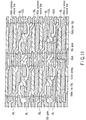
- the two sense amplifier transistors constituting the differential amplifier circuit (Q16 and Q17 in FIG. 1), cross-coupled between paired bit lines, form a pattern such that, when it were moved in parallel, one of the two transistors could be superimposed upon the other with respect to diffused regions, gate wirings and contacts from first metal lines to the diffused regions.
- the two DQ gate transistors (Q18 and Q19 in FIG. 1) connected to the same paired bit lines also form the above described superimposable pattern with parallel movement.
- the diffusion area on the BL side of the sense amplifier and the diffusion area on the BL side of the DQ gate consist of a common diffusion area.
- the diffusion area on the /BL side of the sense amplifier and the diffusion area on the /BL side of the DQ gate consist of a common diffusion area.
- the paired bit lines BL and /BL, the NSA common source lines and the data lines, which are all first metal interconnect lines, are represented by lower-right-pointing oblique parallel lines.
- the gate interconnect lines and the column select lines CSL are represented by upper-right-pointing oblique parallel lines.
- the two sense amplifier transistors arranged adjacent to each other in the above described superimposable pattern layout, are each indicated by broken line.
- the two DQ gate transistors which are also arranged in the superimposable pattern layout above the sense amplifier transistors, are each indicated by broken line.
- Another pair of sense amplifier transistors and another pair of DQ gate transistors are arranged above the arrangement of the aforesaid first pairs of sense amplifier transistors and DQ gate transistors.
- the pattern layout of the pair of DQ gate transistors connected to each bit line pair and the pattern layout of another pair of DQ gate transistors connected to the adjacent bit line pair are symmetrical with respect to a point in the pattern layout of the sense amplifier.
- the diffusion areas, each of which is shared between corresponding sense amplifier and DQ gate transistors are formed in portions of the semiconductor substrate which are just below the paired bit lines BL and /BL.
- the NSA and the DQ gate are shown as one block; however, they are actually laid out as shown in FIG. 11.
- two transistors constituting an NSA are each formed into a perfectly superimposable pattern with parallel movement. That is, with respect to patterns of active regions (diffused regions), gate interconnection, and contacts to the active regions, one of the two transistors could be completely superimposed upon the other if it were moved in parallel.
- the two DQ gate transistors are each formed in a perfectly superimposable pattern with parallel movement.
- Such a superimposable pattern has become feasible by connecting the pair of bit lines BL, /BL comprising the first metal to the gate wirings of the sense amplifier transistors on the semiconductor substrate so as to twist each other.
- the sense amplifier layout is required to be small in its size in the direction in which the bit lines extend in the narrow region defined by the period of arrangement of the bit lines.
- This advantage also results from connecting the paired bit lines BL and /BL with the gate interconnections of the sense transistors in a twisted manner in the sense amplifier layout to thereby reduce the density of the first metal interconnect lines.
- the parasitic capacitance associated with the bit lines can be reduced in comparison with the case where separate diffusion areas are provided, which also helps enhance the amplifying capability.
- the tenth embodiment can provide a sense amplifier for use in a semiconductor memory device which is great in the margin of mask misalignment, high in the small-signal amplifying capability, and small in the layout size.
- the common sources of two transistors constituting the NSA are directly connected together by a first metal interconnect line as shown in FIG. 11, the potential difference between the common sources of the transistors can be reduced to a minimum at sense time.
- the small-signal amplifying capability can be enhanced further.
- the present invention may be practiced or embodied in still other ways without departing from the scope and spirit thereof.
- the layout size of the entire sense amplifier section including control circuits can be reduced by forming the set driver for a sense amplifier from both an NFET and a PFET or by forming the PSA set driver from an NFET and the NSA set driver from a PFET.
- a semiconductor memory device can be implemented which is small in chip size, high in small-signal amplifying capability, and highly competitive in cost.
Landscapes
- Engineering & Computer Science (AREA)
- Microelectronics & Electronic Packaging (AREA)
- Computer Hardware Design (AREA)
- Dram (AREA)
- Semiconductor Memories (AREA)
- Static Random-Access Memory (AREA)
Applications Claiming Priority (2)
| Application Number | Priority Date | Filing Date | Title |
|---|---|---|---|
| JP2001000475 | 2001-01-05 | ||
| JP2001000475A JP2002208277A (ja) | 2001-01-05 | 2001-01-05 | 半導体記憶装置のセンスアンプ制御回路 |
Publications (2)
| Publication Number | Publication Date |
|---|---|
| EP1237160A2 true EP1237160A2 (de) | 2002-09-04 |
| EP1237160A3 EP1237160A3 (de) | 2004-09-01 |
Family
ID=18869257
Family Applications (1)
| Application Number | Title | Priority Date | Filing Date |
|---|---|---|---|
| EP01131050A Withdrawn EP1237160A3 (de) | 2001-01-05 | 2001-12-31 | Leseverstärkersteuerschaltung für Halbleiterspeicheranordnung |
Country Status (6)
| Country | Link |
|---|---|
| US (2) | US6496435B2 (de) |
| EP (1) | EP1237160A3 (de) |
| JP (1) | JP2002208277A (de) |
| KR (1) | KR100412000B1 (de) |
| CN (4) | CN1302551C (de) |
| TW (1) | TW530407B (de) |
Families Citing this family (17)
| Publication number | Priority date | Publication date | Assignee | Title |
|---|---|---|---|---|
| US6071689A (en) * | 1997-12-31 | 2000-06-06 | Xy, Inc. | System for improving yield of sexed embryos in mammals |
| WO2003039421A2 (en) * | 2001-11-05 | 2003-05-15 | The Procter & Gamble Company | Stretch composites and methods of making the composite |
| DE10310570B3 (de) * | 2003-03-11 | 2004-09-30 | Infineon Technologies Ag | Verfahren und Testschaltung zum Testen einer dynamischen Speicherschaltung |
| JP2005322380A (ja) | 2004-04-09 | 2005-11-17 | Toshiba Corp | 半導体記憶装置 |
| US7448012B1 (en) | 2004-04-21 | 2008-11-04 | Qi-De Qian | Methods and system for improving integrated circuit layout |
| US7664796B2 (en) * | 2004-10-13 | 2010-02-16 | Microsoft Corporation | Electronic labeling for offline management of storage devices |
| FR2879816B1 (fr) * | 2004-12-20 | 2007-06-08 | Atmel Nantes Sa Sa | Circuit electronique comprenant au moins une premiere et une seconde paires differentielles dont les transistors partagent un meme caisson |
| FR2879817B1 (fr) * | 2004-12-20 | 2007-03-30 | Atmel Nantes Sa Sa | Circuit electronique comprenant au moins une premiere paire differentielle dont les transistors partagent une meme source ou un meme drain |
| KR100656470B1 (ko) | 2006-02-07 | 2006-12-11 | 주식회사 하이닉스반도체 | 반도체 메모리의 드라이버 제어장치 및 방법 |
| JP5248019B2 (ja) * | 2007-01-09 | 2013-07-31 | エルピーダメモリ株式会社 | 半導体記憶装置、及びそのセンスアンプ回路 |
| KR100866146B1 (ko) | 2007-10-11 | 2008-10-31 | 주식회사 하이닉스반도체 | 센스 앰프 제어 회로 |
| JP5711033B2 (ja) * | 2011-04-12 | 2015-04-30 | ルネサスエレクトロニクス株式会社 | 半導体集積回路装置 |
| US8693236B2 (en) | 2011-12-09 | 2014-04-08 | Gsi Technology, Inc. | Systems and methods of sectioned bit line memory arrays, including hierarchical and/or other features |
| US8593860B2 (en) | 2011-12-09 | 2013-11-26 | Gsi Technology, Inc. | Systems and methods of sectioned bit line memory arrays |
| JP2014017386A (ja) * | 2012-07-10 | 2014-01-30 | Ps4 Luxco S A R L | 半導体装置 |
| CN109991806B (zh) * | 2017-12-29 | 2022-03-11 | 长鑫存储技术有限公司 | 掩膜版、存储器及存储器的制造方法 |
| US11495282B2 (en) | 2020-08-12 | 2022-11-08 | Micron Technology, Inc. | Sense amplifier drivers, and related devices, systems, and methods |
Family Cites Families (8)
| Publication number | Priority date | Publication date | Assignee | Title |
|---|---|---|---|---|
| KR890004762B1 (ko) * | 1986-11-21 | 1989-11-25 | 삼성전자 주식회사 | 고성능 디램을 위한 센스 증폭기 |
| KR910009551B1 (ko) * | 1988-06-07 | 1991-11-21 | 삼성전자 주식회사 | 메모리장치의 센스앰프 분할 제어회로 |
| JPH0758594B2 (ja) * | 1988-12-27 | 1995-06-21 | シャープ株式会社 | ダイナミック型半導体記憶装置 |
| KR920010346B1 (ko) * | 1990-05-23 | 1992-11-27 | 삼성전자 주식회사 | 반도체 메모리의 센스앰프 구동회로 |
| JP3549602B2 (ja) * | 1995-01-12 | 2004-08-04 | 株式会社ルネサステクノロジ | 半導体記憶装置 |
| US5636158A (en) | 1995-03-13 | 1997-06-03 | Kabushiki Kaisha Toshiba | Irregular pitch layout for a semiconductor memory device |
| JPH10284705A (ja) * | 1997-04-10 | 1998-10-23 | Hitachi Ltd | ダイナミック型ram |
| JP2001077322A (ja) | 1999-09-02 | 2001-03-23 | Toshiba Corp | 半導体集積回路装置 |
-
2001
- 2001-01-05 JP JP2001000475A patent/JP2002208277A/ja active Pending
- 2001-12-27 US US10/035,043 patent/US6496435B2/en not_active Expired - Lifetime
- 2001-12-30 CN CNB2004100460001A patent/CN1302551C/zh not_active Expired - Lifetime
- 2001-12-30 CN CNA2006101156987A patent/CN1956198A/zh active Pending
- 2001-12-30 CN CNA2004101003925A patent/CN1624796A/zh active Pending
- 2001-12-30 CN CN01138188A patent/CN1372268A/zh active Pending
- 2001-12-31 TW TW090133233A patent/TW530407B/zh not_active IP Right Cessation
- 2001-12-31 EP EP01131050A patent/EP1237160A3/de not_active Withdrawn
-
2002
- 2002-01-05 KR KR10-2002-0000616A patent/KR100412000B1/ko not_active Expired - Lifetime
- 2002-10-09 US US10/267,949 patent/US6674678B2/en not_active Expired - Lifetime
Also Published As
| Publication number | Publication date |
|---|---|
| CN1542972A (zh) | 2004-11-03 |
| US6496435B2 (en) | 2002-12-17 |
| US20020089888A1 (en) | 2002-07-11 |
| JP2002208277A (ja) | 2002-07-26 |
| KR20020057830A (ko) | 2002-07-12 |
| CN1372268A (zh) | 2002-10-02 |
| CN1624796A (zh) | 2005-06-08 |
| CN1302551C (zh) | 2007-02-28 |
| TW530407B (en) | 2003-05-01 |
| CN1956198A (zh) | 2007-05-02 |
| US6674678B2 (en) | 2004-01-06 |
| KR100412000B1 (ko) | 2003-12-24 |
| US20030031071A1 (en) | 2003-02-13 |
| EP1237160A3 (de) | 2004-09-01 |
Similar Documents
| Publication | Publication Date | Title |
|---|---|---|
| US6496435B2 (en) | Sense amplifier control circuit of semiconductor memory device | |
| US6504204B1 (en) | Compact dual-port DRAM architecture system and method for making same | |
| US6600671B2 (en) | Reduced area sense amplifier isolation layout in a dynamic RAM architecture | |
| US7842976B2 (en) | Semiconductor device having MOS transistors which are serially connected via contacts and conduction layer | |
| US6034879A (en) | Twisted line techniques for multi-gigabit dynamic random access memories | |
| US6392942B2 (en) | Semiconductor memory device having a multi-layer interconnection structure suitable for merging with logic | |
| KR20080065529A (ko) | 반도체 기억장치 및 그 센스 증폭기 회로 | |
| US6319800B1 (en) | Static memory cell | |
| US20070158695A1 (en) | System with meshed power and signal buses on cell array | |
| KR100283542B1 (ko) | 입력 신호의 오버슈트, 언더슈트를 피엔 접합을 이용한 회로에의해 클램프하는 반도체 기억 장치 | |
| CA2195836C (en) | Semiconductor memory having main word line and subword lines provided correspondingly to the main word line | |
| JPH0752757B2 (ja) | 半導体記憶装置 | |
| KR100466689B1 (ko) | 콤팩트형 이중 포트 동적 랜덤 액세스 메모리 아키텍쳐 시스템 및 그 제조 방법 | |
| US5386127A (en) | Semiconductor device having groups of pads which receive the same signal | |
| US11646347B2 (en) | Semiconductor device having transistors in which source/drain regions are shared | |
| US6222784B1 (en) | Semiconductor memory | |
| US6166976A (en) | Multiple equilibration circuits for a single bit line | |
| US7782647B2 (en) | Semiconductor memory device | |
| KR100301542B1 (ko) | 단일칩 메모리 시스템 | |
| KR20040041097A (ko) | 센스 증폭기 및 오픈 디지트 어레이의 구조 | |
| US6396756B1 (en) | Integrated circuit memory devices including transmission parts that are adjacent input/output selection parts | |
| KR20020071181A (ko) | 계층적 비트 라인 구조를 갖는 반도체 메모리 소자 | |
| US5140555A (en) | Semiconductor integrated device having uniform noise between a pair of undecided voltage portions | |
| Miyamoto et al. | A fast 256/spl times/4 CMOS DRAM with a distributed sense and unique restore circuit | |
| US5978287A (en) | Input/output device having shared active area |
Legal Events
| Date | Code | Title | Description |
|---|---|---|---|
| PUAI | Public reference made under article 153(3) epc to a published international application that has entered the european phase |
Free format text: ORIGINAL CODE: 0009012 |
|
| 17P | Request for examination filed |
Effective date: 20011231 |
|
| AK | Designated contracting states |
Kind code of ref document: A2 Designated state(s): AT BE CH CY DE DK ES FI FR GB GR IE IT LI LU MC NL PT SE TR |
|
| AX | Request for extension of the european patent |
Free format text: AL;LT;LV;MK;RO;SI |
|
| RIC1 | Information provided on ipc code assigned before grant |
Ipc: 7G 11C 11/405 B Ipc: 7G 11C 11/4091 B Ipc: 7G 11C 7/06 A |
|
| PUAL | Search report despatched |
Free format text: ORIGINAL CODE: 0009013 |
|
| AK | Designated contracting states |
Kind code of ref document: A3 Designated state(s): AT BE CH CY DE DK ES FI FR GB GR IE IT LI LU MC NL PT SE TR |
|
| AX | Request for extension of the european patent |
Extension state: AL LT LV MK RO SI |
|
| AKX | Designation fees paid |
Designated state(s): DE FR GB |
|
| RBV | Designated contracting states (corrected) |
Designated state(s): DE FR GB |
|
| 17Q | First examination report despatched |
Effective date: 20071128 |
|
| STAA | Information on the status of an ep patent application or granted ep patent |
Free format text: STATUS: THE APPLICATION IS DEEMED TO BE WITHDRAWN |
|
| 18D | Application deemed to be withdrawn |
Effective date: 20080409 |