EP1207970B1 - Elektrostatischer ultraschallwandler und verfahren zu dessen herstellung - Google Patents
Elektrostatischer ultraschallwandler und verfahren zu dessen herstellung Download PDFInfo
- Publication number
- EP1207970B1 EP1207970B1 EP00930807A EP00930807A EP1207970B1 EP 1207970 B1 EP1207970 B1 EP 1207970B1 EP 00930807 A EP00930807 A EP 00930807A EP 00930807 A EP00930807 A EP 00930807A EP 1207970 B1 EP1207970 B1 EP 1207970B1
- Authority
- EP
- European Patent Office
- Prior art keywords
- transducer
- electrodes
- insulating film
- layer
- sacrificial
- Prior art date
- Legal status (The legal status is an assumption and is not a legal conclusion. Google has not performed a legal analysis and makes no representation as to the accuracy of the status listed.)
- Expired - Lifetime
Links
- 238000004519 manufacturing process Methods 0.000 title claims description 7
- 238000000151 deposition Methods 0.000 claims description 21
- 239000011800 void material Substances 0.000 claims description 20
- 238000000034 method Methods 0.000 claims description 19
- 239000000758 substrate Substances 0.000 claims description 18
- 239000012212 insulator Substances 0.000 claims description 16
- 239000000463 material Substances 0.000 claims description 15
- 239000004020 conductor Substances 0.000 claims description 11
- 238000005530 etching Methods 0.000 claims description 10
- XAGFODPZIPBFFR-UHFFFAOYSA-N aluminium Chemical compound [Al] XAGFODPZIPBFFR-UHFFFAOYSA-N 0.000 claims description 5
- 229910052782 aluminium Inorganic materials 0.000 claims description 5
- 230000037361 pathway Effects 0.000 claims description 5
- 238000000623 plasma-assisted chemical vapour deposition Methods 0.000 claims description 5
- 229910052581 Si3N4 Inorganic materials 0.000 claims description 4
- 239000010949 copper Substances 0.000 claims description 4
- HQVNEWCFYHHQES-UHFFFAOYSA-N silicon nitride Chemical compound N12[Si]34N5[Si]62N3[Si]51N64 HQVNEWCFYHHQES-UHFFFAOYSA-N 0.000 claims description 4
- RYGMFSIKBFXOCR-UHFFFAOYSA-N Copper Chemical compound [Cu] RYGMFSIKBFXOCR-UHFFFAOYSA-N 0.000 claims description 3
- 229910052802 copper Inorganic materials 0.000 claims description 3
- 229910052710 silicon Inorganic materials 0.000 claims description 3
- 239000010703 silicon Substances 0.000 claims description 3
- WFKWXMTUELFFGS-UHFFFAOYSA-N tungsten Chemical compound [W] WFKWXMTUELFFGS-UHFFFAOYSA-N 0.000 claims description 3
- 229910052721 tungsten Inorganic materials 0.000 claims description 3
- 239000010937 tungsten Substances 0.000 claims description 3
- VYPSYNLAJGMNEJ-UHFFFAOYSA-N Silicium dioxide Chemical compound O=[Si]=O VYPSYNLAJGMNEJ-UHFFFAOYSA-N 0.000 claims 1
- 239000004411 aluminium Substances 0.000 claims 1
- 229910052814 silicon oxide Inorganic materials 0.000 claims 1
- 239000012528 membrane Substances 0.000 description 17
- 230000003071 parasitic effect Effects 0.000 description 13
- PCHJSUWPFVWCPO-UHFFFAOYSA-N gold Chemical compound [Au] PCHJSUWPFVWCPO-UHFFFAOYSA-N 0.000 description 10
- 229910052737 gold Inorganic materials 0.000 description 10
- 239000010931 gold Substances 0.000 description 10
- 150000004767 nitrides Chemical class 0.000 description 10
- 230000008569 process Effects 0.000 description 3
- 239000004065 semiconductor Substances 0.000 description 3
- IJGRMHOSHXDMSA-UHFFFAOYSA-N Atomic nitrogen Chemical compound N#N IJGRMHOSHXDMSA-UHFFFAOYSA-N 0.000 description 2
- KRHYYFGTRYWZRS-UHFFFAOYSA-N Fluorane Chemical compound F KRHYYFGTRYWZRS-UHFFFAOYSA-N 0.000 description 2
- XUIMIQQOPSSXEZ-UHFFFAOYSA-N Silicon Chemical compound [Si] XUIMIQQOPSSXEZ-UHFFFAOYSA-N 0.000 description 2
- 239000003990 capacitor Substances 0.000 description 2
- 238000007654 immersion Methods 0.000 description 2
- 230000004048 modification Effects 0.000 description 2
- 238000012986 modification Methods 0.000 description 2
- 238000000926 separation method Methods 0.000 description 2
- 230000015572 biosynthetic process Effects 0.000 description 1
- 230000008859 change Effects 0.000 description 1
- 238000006243 chemical reaction Methods 0.000 description 1
- 230000007547 defect Effects 0.000 description 1
- 230000008021 deposition Effects 0.000 description 1
- 230000001066 destructive effect Effects 0.000 description 1
- 238000001514 detection method Methods 0.000 description 1
- 238000002059 diagnostic imaging Methods 0.000 description 1
- 238000010586 diagram Methods 0.000 description 1
- 230000005684 electric field Effects 0.000 description 1
- 238000011156 evaluation Methods 0.000 description 1
- 239000007789 gas Substances 0.000 description 1
- 239000007788 liquid Substances 0.000 description 1
- 229910052757 nitrogen Inorganic materials 0.000 description 1
- 230000008447 perception Effects 0.000 description 1
- 229910021420 polycrystalline silicon Inorganic materials 0.000 description 1
- 229920005591 polysilicon Polymers 0.000 description 1
- 230000009467 reduction Effects 0.000 description 1
- 230000004044 response Effects 0.000 description 1
- 238000007789 sealing Methods 0.000 description 1
- 238000006467 substitution reaction Methods 0.000 description 1
- 230000002463 transducing effect Effects 0.000 description 1
Images




Classifications
-
- G—PHYSICS
- G01—MEASURING; TESTING
- G01H—MEASUREMENT OF MECHANICAL VIBRATIONS OR ULTRASONIC, SONIC OR INFRASONIC WAVES
- G01H11/00—Measuring mechanical vibrations or ultrasonic, sonic or infrasonic waves by detecting changes in electric or magnetic properties
- G01H11/06—Measuring mechanical vibrations or ultrasonic, sonic or infrasonic waves by detecting changes in electric or magnetic properties by electric means
-
- B—PERFORMING OPERATIONS; TRANSPORTING
- B06—GENERATING OR TRANSMITTING MECHANICAL VIBRATIONS IN GENERAL
- B06B—METHODS OR APPARATUS FOR GENERATING OR TRANSMITTING MECHANICAL VIBRATIONS OF INFRASONIC, SONIC, OR ULTRASONIC FREQUENCY, e.g. FOR PERFORMING MECHANICAL WORK IN GENERAL
- B06B1/00—Methods or apparatus for generating mechanical vibrations of infrasonic, sonic, or ultrasonic frequency
- B06B1/02—Methods or apparatus for generating mechanical vibrations of infrasonic, sonic, or ultrasonic frequency making use of electrical energy
- B06B1/0292—Electrostatic transducers, e.g. electret-type
-
- Y—GENERAL TAGGING OF NEW TECHNOLOGICAL DEVELOPMENTS; GENERAL TAGGING OF CROSS-SECTIONAL TECHNOLOGIES SPANNING OVER SEVERAL SECTIONS OF THE IPC; TECHNICAL SUBJECTS COVERED BY FORMER USPC CROSS-REFERENCE ART COLLECTIONS [XRACs] AND DIGESTS
- Y10—TECHNICAL SUBJECTS COVERED BY FORMER USPC
- Y10T—TECHNICAL SUBJECTS COVERED BY FORMER US CLASSIFICATION
- Y10T29/00—Metal working
- Y10T29/42—Piezoelectric device making
-
- Y—GENERAL TAGGING OF NEW TECHNOLOGICAL DEVELOPMENTS; GENERAL TAGGING OF CROSS-SECTIONAL TECHNOLOGIES SPANNING OVER SEVERAL SECTIONS OF THE IPC; TECHNICAL SUBJECTS COVERED BY FORMER USPC CROSS-REFERENCE ART COLLECTIONS [XRACs] AND DIGESTS
- Y10—TECHNICAL SUBJECTS COVERED BY FORMER USPC
- Y10T—TECHNICAL SUBJECTS COVERED BY FORMER US CLASSIFICATION
- Y10T29/00—Metal working
- Y10T29/49—Method of mechanical manufacture
- Y10T29/49002—Electrical device making
- Y10T29/49005—Acoustic transducer
-
- Y—GENERAL TAGGING OF NEW TECHNOLOGICAL DEVELOPMENTS; GENERAL TAGGING OF CROSS-SECTIONAL TECHNOLOGIES SPANNING OVER SEVERAL SECTIONS OF THE IPC; TECHNICAL SUBJECTS COVERED BY FORMER USPC CROSS-REFERENCE ART COLLECTIONS [XRACs] AND DIGESTS
- Y10—TECHNICAL SUBJECTS COVERED BY FORMER USPC
- Y10T—TECHNICAL SUBJECTS COVERED BY FORMER US CLASSIFICATION
- Y10T29/00—Metal working
- Y10T29/49—Method of mechanical manufacture
- Y10T29/49002—Electrical device making
- Y10T29/49007—Indicating transducer
-
- Y—GENERAL TAGGING OF NEW TECHNOLOGICAL DEVELOPMENTS; GENERAL TAGGING OF CROSS-SECTIONAL TECHNOLOGIES SPANNING OVER SEVERAL SECTIONS OF THE IPC; TECHNICAL SUBJECTS COVERED BY FORMER USPC CROSS-REFERENCE ART COLLECTIONS [XRACs] AND DIGESTS
- Y10—TECHNICAL SUBJECTS COVERED BY FORMER USPC
- Y10T—TECHNICAL SUBJECTS COVERED BY FORMER US CLASSIFICATION
- Y10T29/00—Metal working
- Y10T29/49—Method of mechanical manufacture
- Y10T29/49002—Electrical device making
- Y10T29/4902—Electromagnet, transformer or inductor
- Y10T29/4908—Acoustic transducer
-
- Y—GENERAL TAGGING OF NEW TECHNOLOGICAL DEVELOPMENTS; GENERAL TAGGING OF CROSS-SECTIONAL TECHNOLOGIES SPANNING OVER SEVERAL SECTIONS OF THE IPC; TECHNICAL SUBJECTS COVERED BY FORMER USPC CROSS-REFERENCE ART COLLECTIONS [XRACs] AND DIGESTS
- Y10—TECHNICAL SUBJECTS COVERED BY FORMER USPC
- Y10T—TECHNICAL SUBJECTS COVERED BY FORMER US CLASSIFICATION
- Y10T29/00—Metal working
- Y10T29/49—Method of mechanical manufacture
- Y10T29/49002—Electrical device making
- Y10T29/49117—Conductor or circuit manufacturing
- Y10T29/49124—On flat or curved insulated base, e.g., printed circuit, etc.
- Y10T29/49155—Manufacturing circuit on or in base
- Y10T29/49156—Manufacturing circuit on or in base with selective destruction of conductive paths
Definitions
- the present invention relates to the field of acoustic transducers, and in preferred embodiments to a novel electrostatic ultrasonic transducer capable of operating in high frequency ranges, and novel methods of fabricating such a transducer.
- An acoustic transducer is an electronic device used to emit and receive sound waves.
- An ultrasonic transducer is a type of acoustic transducer that operates at a frequency range beyond that of human perception, about 20 KHz.
- Acoustic transducers are used in medical imaging, non-destructive evaluation, and other applications.
- the most common forms of acoustic transducers are piezoelectric transducers, which operate in low and narrow band frequencies. Piezoelectric transducers are not efficient in the conversion between electric and acoustic energy in air. Furthermore, the operating frequencies of piezoelectric transducers in air are quite low.
- Air coupled ultrasonic transducers with higher operating frequencies which rely on certain microfabrication techniques, are described by Haller et al. in U.S. Patent No. 5,619,476 entitled “Electrostatic Ultrasonic Transducer,” issued April 9, 1997, and Ladabaum et al. in U.S. Patent No. 5,870,351 entitled “Broadband Microfabricated Ultrasonic Transducer and Method of Fabrication,” issued February 9, 1999. Published material known in the art also demonstrates that immersion transducers can be made with similar techniques. Air-coupled transducers are usually resonant, while liquid-coupled transducers are typically not. As shown in FIGS.
- the transducer disclosed therein is made of a substrate 11 and a gold contact layer 14 that forms one plate of a capacitor, and a membrane including a nitride layer 13 and a gold contact layer 14B that form the other plate of the capacitor (while the gold contact layer 14 is the electrode, with the nitride layer 13 being an insulator, the reference to electrode 13/14 will be used so as to distinguish the other electrode 11/14 that has a gold contact layer 14 adjacent the conductive substrate 11 as illustrated in the above-mentioned patents).
- Holes 16 etched in the nitride layer 13 and the gold layer 14 are used to etch away portions of the sacrificial oxide layer 12, while remaining posts of the sacrificial layer 12 support the membrane. By noting the change in capacitance between the two electrodes 13/14 and 11/14, the ultrasonic resonance of the membrane can be detected.
- Such microfabricated ultrasonic transducers use resilient membranes that have very little inertia.
- the momentum carried by approximately half of a wavelength of air molecules is able to set the membrane in motion and visa versa.
- Electrostatic actuation and detection enable the realization and control of such resonant membranes. When distances are small, electrostatic attractions can exert very large forces on the actuators of interest.
- Microfabricated ultrasonic transducers of this design have practical problems that prohibit their use at high frequencies, typically above about 10MHz, and that reduce their efficiency at any frequency range. It has been realized by the present inventor that there are various reasons that prohibit the use of microfabricated ultrasonic transducers.
- One reason is that the electrodes 13/14 and 11/14 are each formed as a conductive sheet. As illustrated in FIG. 1A , while the gold contact layer 14 covers the voids where the sacrificial layer 12 has been etched away, the gold contact layer 14 also entirely covers the posts which support the membrane. Similarly, the substrate 11 and the gold contact layer 14 associated therewith is another conductive sheet.
- the spacing between the top electrode 13/14 and the bottom electrode 11/14 is a further reason that the parasitic capacitance increases.
- the membrane has a thickness that, due to physical constraints, needs to be at least about 2,500 Angstroms thick.
- transducers such as those described in Haller et al or Ladabaum et al are not able to operate at higher frequencies, and operate less efficiently than ultimately possible at lower frequencies. Accordingly, there is the need for an improved acoustic transducer.
- JP-A-01312486 discloses an ultrasonic wave array transducer, having a plurality of lower electrodes and a film-like upper electrode.
- a transducer comprising: a supporting substrate; and a transducer cell formed on the substrate, said transducer cell including: a first electrode formed over the substrate; an insulating film formed over the first electrode and including a void region therein; and, a second electrode formed within the insulating film such that the void region is disposed between the first electrode and the second electrode and the thickness of the insulating film is greater than the spacing between the first and second electrode; characterised in that: the first electrode is planar and is disposed at least substantially parallel to the second electrode, and wherein the first and second electrodes each have a surface area of the surface portion parallel to and nearest the void region that is smaller than a surface area of the corresponding surface portion of the void region that is parallel to and nearest each of the electrodes.
- a method of manufacturing a transducer comprising: depositing a first conductive layer on a substrate; etching the first conductive layer to form at least two first electrodes and a first interconnect electrically connecting the at least two first electrodes, the at least two first electrodes being planar; depositing a first insulating film layer of insulator material on the etched conductor; depositing a sacrificial layer over the first insulating film; etching the sacrificial layer to create at least two sacrificial portions, each in substantial alignment with and overlapping one of the two first electrodes; depositing a second insulating film layer of insulator material over the etched sacrificial layer; depositing a second conductive layer over the second insulating film layer, etching the second conductive layer to form at least two second electrodes that respectively overlap and substantially align with and are substantially parallel to the first electrodes, and a second interconnect electrically connecting the two second electrodes wherein the
- the present invention provides an ultrasonic transducer capable of operating at higher frequencies; provides an ultrasonic transducer capable of operating more efficiently than previously known ultrasonic transducers; provides an ultrasonic transducer that has reduced parasitic capacitance between the electrodes used to alternatively detect and excite the sound wave; forms a transducer of a plurality of transducer cells that have an interconnect structure that reduces parasitic capacitance; and, provides a method for fabricating an ultrasonic transducer that has the above-mentioned characteristics.
- the present invention in an embodiment has an ultrasonic transducer comprised of a plurality of transducer cells, and conductive interconnects between the cells.
- Each transducer cell contains a bottom electrode formed on a layer of insulator material, a lower insulating film portion formed over the bottom electrode, a middle insulating film portion that includes an air/vacuum void region, and an upper insulating film portion that includes a top electrode formed within a portion of the upper insulating film portion.
- a first layer of interconnects electrically connect the bottom electrodes of each transducer cell and a second layer of interconnects electrically connect the top electrodes of each transducer cell.
- the top and bottom layers of interconnects are patterned to avoid overlap between them, thus reducing the parasitic capacitance.
- the top electrode is preferably formed within the upper insulating film portion, closer to the air/vacuum void than to the top surface of the insulating film, to increase the electric field for a given voltage.
- the electrodes within each transducer cell are preferably formed to have dimensions that are smaller than the overall surface area of the insulating film that they excite.
- a preferred method of fabricating the ultrasonic transducer according to the invention is initiated by depositing and forming a pattern of the bottom electrode and interconnects. Thereafter, the lower insulating film portion of insulator material is deposited. A sacrificial layer is then deposited over the lower insulating film portion and etched to a desired pattern. The middle insulating film portion of insulator material is deposited over the sacrificial layer pattern, followed by the depositing and forming of the top layer of electrode and interconnects. Thereafter, an upper insulating film portion of insulator material is deposited to complete the formation of the insulating film. Thereafter, the insulating film is etched to form a via hole that allows an etchant to reach the sacrificial layer pattern. Etching is then performed to remove the remaining sacrificial layer pattern to form void areas. Sometimes such via holes and etching is introduced after the middle insulating film portion is deposited and before the top layer of electrode and interconnects is deposited.
- the top layer of electrode and interconnects is formed so that the top layer interconnects do not overlap the bottom layer interconnects, thus reducing the parasitic capacitance.
- the ultrasonic transducer is comprised of a number of interconnected transducer cells.
- the transducer cells are electrically connected together to form a single ultrasonic transducer.
- Multiple transducers can be formed on the same substrate in an array.
- the ultrasonic transducers, and each of the transducer cells formed therein, are formed at the same time using the fabrication steps described above.
- FIG. 2 illustrates a top-view diagram illustrating certain aspects of the present invention.
- a transducer 100 is illustrated as including three connected octagonal-shaped transducer cells 200A-C are shown.
- the transducer 100 may have as few as one or many more than three, such as hundreds or thousands, transducer cells 200 associated with it.
- Many such transducers 100 will typically be formed at the same time on a wafer, with the wafer cut into different die as is known in the art. The discussions hereinafter, however, will be made with respect to a single transducer 100.
- transducer cells 200 illustrated in FIG. 2 is for illustrative purposes, and it is understood that the shape of the transducer cell can be a variety of different shapes, such as hexagonal, round, square, rectangular, triangular, or any other suitable configuration.
- transducer cells 200 may be of different sizes to provide broadband frequency response.
- Transducer cells 200 may also be of certain shapes, such as rectangular, so that they may resonate at a plurality of frequencies. Any number of transducer cells 200 can be interconnected, as described in further detail hereinafter, to form a single transducer.
- top and bottom interconnects 220 and 230 that are used to electrically connect top and bottom electrodes, respectively, of adjacent transducer cells 200.
- the present invention forms transducer cells which each have their own top and bottom electrodes, and then interconnects having dimensions smaller than the entire sheet of conductor are used to electrically connect different electrodes. While the top and bottom electrodes of the various cell transducers can be electrically viewed as being single top and bottom electrodes, the discussion hereinafter will use the top and bottom electrodes to refer to the electrodes associated with a single transducer cell.
- a multi-membrane transducer is formed by interconnecting transducer cells 200A-C on a substrate 300.
- the transducer cells 200 may be of the same size, as shown, or be of different sizes.
- each transducer cell 200 is electrically connected to other transducer cells 200, such that each transducer cell 200 has a top electrode 350 linked by a top layer interconnect 220, as illustrated in FIG. 2 .
- Each bottom electrode 320 (not shown in FIG.
- interconnect 220 and 230 are connected by a bottom layer interconnect 230. Accordingly, overlap of the interconnect 220 and 230 is avoided.
- dielectric constant of semiconductor insulators such as nitride
- the dielectric constant of semiconductor insulators can be approximately one order of magnitude larger than that of the air/vacuum, by eliminating, or at least minimizing, overlap of the electrode interconnects, parasitic capacitance is reduced.
- FIG. 3 illustrates a cross-section taken along line 3-3 of Fig 2 of the plurality of transducer cells 200A-C.
- Each transducer cell 200 is contains an air/vacuum cavity 340 surrounded by an insulative insulating film layer 330, with a bottom electrode 320 and a top electrode 350 associated with each transducer cell 200.
- FIG. 3 Another aspect of the present invention is illustrated in FIG. 3 , with reference to the relative dimensions R, S, and D illustrated in FIG. 3 .
- the dimension R is the thickness of the membrane, which is formed of a portion of the insulating layer 330 and the top electrode disposed therein, that is disposed above the air/vacuum cavity 340 and that is required for a certain acoustic impedance of the transducer cells, such impedance governing the frequency range of the transducer.
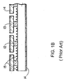
- FIG. 1B illustrates a certain known microfabricated electronic transducer that uses a gold contact layer 14 fabricated on the top surface of the nitride layer 13 as a top electrode of the transducer.
- the nitride layer 13 illustrated in FIG. 1B and the membrane of the present invention both must operate in the frequency range of interest, as described previously.
- the present invention forms the top electrode 350 within the membrane. Accordingly, whereas the separation distance of the bottom and the top electrodes is D in the prior art electronic transducer described in FIG. 1B , the separation distance of the bottom and top electrodes according to the present invention is S. Since the top electrode is formed within the membrane, the distance S will, for an otherwise equivalent transducer, always be less than D. By forming the top electrode within the membrane, as described fully hereinafter, parasitic capacitance in the present invention is further reduced.
- FIGS. 2 and 3 Another aspect of the invention illustrated by FIGS. 2 and 3 is that the surface area of the electrodes 320 and 350 is smaller than the surface area of the corresponding air/vacuum cavity 340. As noted hereinafter, this further allows for a reduction in the parasitic capacitance of the resulting ultrasonic transducer.
- the transducer cells 200 according to the present invention can have a variety of shapes and dimensions.
- membrane will typically have an area that ranges from about 300 to 30,000 ⁇ m 2 with a membrane thickness that ranges from about 0.05 to I ⁇ m, a residual stress in the PECVD nitride ranging from about 10 to 400 MPa and a gap thickness ranging from about 0.1 to 2 ⁇ m. It is understood, however, that these dimensions are illustrative only and that any dimensions which meet the characteristics of the invention described herein can be used, as previously mentioned.
- the process begins with a silicon or other semiconductor support substrate 300. Thereafter, a layer of thermal oxide 310 is grown, preferably having a thickness in the range of 5,000-10,000 ⁇ , followed by a deposition of a conductor 320, which may, for example, have a thickness in the range of 2,500 - 5,000 ⁇ .
- this conductor is aluminum (Al), but the conductor could also be any conductor known in the art, such as copper (Cu) or tungsten (W) or polysilicon.
- a resist pattern is transferred lithographically to the substrate, and the conductor 320 is etched to leave behind a patterned bottom electrodes 350 and associated interconnects.
- FIG. 5 illustrates the resultant patterned bottom electrodes 350A-C and Fig 2 illustrates the resultant patterned bottom interconnect.
- a lower insulating film portion 330A of the insulating film 330 is deposited.
- This lower insulating film portion 330A is an insulator, such as nitride, applied using, for instance a plasma-enhanced chemical vapor deposition (also known as "PECVD").
- PECVD plasma-enhanced chemical vapor deposition
- the applied lower insulating film portion 330A will typically have a measured residual stress that is less than 50 MPas. The residual stress may be adjusted by varying the frequency of the plasma and the relative concentration of nitrogen and silicon carrying gases.
- the lower insulating film portion 330A will typically be deposited to a thickness of about 0.25 ⁇ m.
- the deposited lower insulating film portion 330A will typically not be planarized, instead having a substantially even thickness over the various surfaces, so that the contours of the surface to which the lower insulating film portion 330 is applied will continue to perpetuate through the application of subsequently applied layers, as is known in the art. Planarization can be used, but is not necessary and often introduces substantial additional cost and potential for defects. Accordingly, since this phenomenon is well understood, it will not be described further hereinafter.
- a sacrificial layer 700 as known in the art, such as aluminum or low temperature oxide (LTO), is deposited.
- the deposit thickness may range from 0.05 to 1 ⁇ m.
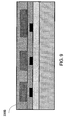
- a resist pattern is transferred lithographically, and the sacrificial layer 700 is etched to leave behind a pattern, such as shown in FIG. 8 .
- the sacrificial layer contains portions 700A, 700B and 700C, which will each correspond to a void region that will be made within each transducer cell 200A, 200B and 200C, respectively.
- a pathway 702 which pathway 702 will allow for the etchant that removes the sacrificial layer to be introduced from a location that is physically separate from the transducer cells.
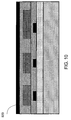
- a middle insulating film portion 330B is then deposited, preferably an insulator that is the same as that of the lower insulating film portion 330A.
- PECVD silicon nitride is deposited as the middle insulating film portion 330B to a thickness of about 0.15 ⁇ m over the patterned sacrificial layer 700 to surround and cover the patterned sacrificial layer 700, as illustrated by FIG. 9 .
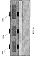
- the top conductor layer 920 is deposited, and subsequently etched in a pattern to produce a top electrode 350 and the resulting interconnects, as shown in FIGS. 3 and 11 and described previously.
- the electrodes 320A, 320B and 320C will overlap the electrodes 350A, 350B and 350C, respectively, the top interconnects 220 will not overlap with the bottom interconnects 230, as described previously. This is ensured by selection of an appropriate pattern for the top and bottom interconnects, one such pattern being illustrated in FIG. 2 .
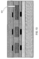
- top insulating film portion 330C of the insulating film 330 is then deposited, as shown in Fig 12 , and the material for the top insulating film portion 330C is preferably the same as that used for the bottom insulating film portion 330A and the middle insulating film portion 330B, previously described.
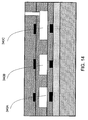
- via holes 900 are created to provide for an etchant path to the remaining portions of the sacrificial layer, such as portions 700A, 700B, 700C and 702 illustrated in FIG. 8 .
- the remaining portions of the sacrificial layer are then etched away by a sacrificial wet etch or other technique known in the art.
- buffered hydrofluoric acid can be used in the case of a low temperature oxide (LTO) sacrificial layer 700.
- the sacrificial etch results in an air/vacuum cavities being formed, such as the cavities 340A, 340B and 340C illustrated in FIG. 14 .
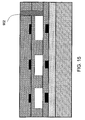
- the via holes 900 can be filled in, preferably using the same material as the insulating film 330, if needed, such as for an immersion transducer.
- the additional material added over the top insulating film portion 330C can also become part of the insulating film 330, or it can be subsequently etched from all areas except for the sealing locations.
Landscapes
- Physics & Mathematics (AREA)
- General Physics & Mathematics (AREA)
- Engineering & Computer Science (AREA)
- Mechanical Engineering (AREA)
- Transducers For Ultrasonic Waves (AREA)
- Apparatuses For Generation Of Mechanical Vibrations (AREA)
- Pressure Sensors (AREA)
- Electrostatic, Electromagnetic, Magneto- Strictive, And Variable-Resistance Transducers (AREA)
Claims (23)
- Wandler (100), umfassend:ein Trägersubstrat (300); undeine Wandlerzelle (200), die auf dem Substrat (300) gebildet ist, wobei die Wandlerzelle (200) beinhaltet:eine erste Elektrode (320), die über dem Substrat (300) gebildet ist;einen Isolierfilm (330), der über der ersten Elektrode (320) gebildet ist und einen Hohlraum (340) darin beinhaltet; undeine zweite Elektrode (350), die innerhalb des Isolierfilms (330) gebildet ist, so dass der Hohlraum (340) zwischen der ersten Elektrode (320) und der zweiten Elektrode (350) angeordnet ist und die Dicke des Isolierfilms (330) größer als der Abstand zwischen der ersten und der zweiten Elektrode (320, 350) ist; dadurch gekennzeichnet, dassdie erste Elektrode (320) flach ist und zumindest im Wesentlichen parallel zur zweiten Elektrode (350) angeordnet ist,und wobei die ersten und zweiten Elektrode (320, 350) jeweils einen Oberflächenbereich des Oberflächenabschnitts, der parallel und am nächsten gelegen zu dem Hohlraum (340) ist, haben, welcher kleiner als ein Oberflächenbereich des entsprechenden Oberflächenabschnitts des Hohlraums (340) ist, der parallel und am nächsten gelegen zu den einzelnen Elektroden (320, 350) ist.
- Wandler (100) nach Anspruch 1, welcher ein Isoliermaterial (310) beinhaltet, welches zwischen dem Substrat (300) und der Wandlerzelle (200) angeordnet ist.
- Wandler (100) nach Anspruch 1 oder 2, wobei der Isolierfilm (330) aus Siliziumnitrid besteht.
- Wandler (100) nach Anspruch 2, wobei das Substrat (300) aus Silizium, das Isoliermaterial (310) aus Siliziumoxid und der Isolierfilm aus Siliziumnitrid besteht.
- Wandler (100) nach einem der Ansprüche 1 bis 4, wobei die ersten und zweiten Elektroden (320, 350) jeweils einen entsprechenden Abschnitt des Isolierfilms (330) haben, der zwischen jeder äußeren Elektrodenoberfläche und dem Hohlraum (340) angeordnet ist.
- Akustischer Wandler (100), umfassend:mindestens zwei Wandlerzellen (200) nach einem der Ansprüche 1 bis 5, die auf dem Substrat (300) gebildet sind, wobei jede Wandlerzelle (200) akustische Signale übertragen und empfangen kann;eine erste Verbindung (230), die die ersten Elektroden (320) jeder der mindestens zwei Wandlerzellen (200) elektrisch miteinander verbindet; undeine zweite Verbindung (220), die die zweiten Elektroden (350) jeder der mindestens zwei Wandlerzellen (200) elektrisch miteinander verbindet;wobei die ersten und zweiten Verbindungen (220, 230) sich im Wesentlichen nicht überlappen.
- Wandler (100) nach Anspruch 6, wobei keine Überlappung der ersten und zweiten Verbindungen (220, 230) in Bereichen stattfindet, die die Hohlräume (340) nicht überlappen.
- Wandler (100) nach Anspruch 6 oder 7, wobei die ersten und zweiten Verbindungen (230, 220) auf derselben Leiterschicht wie die ersten bzw. zweiten Elektroden (320, 350) gebildet sind.
- Wandler (100) nach einem der Ansprüche 6 bis 8, wobei die ersten und zweiten Elektroden (320, 350) und die ersten und zweiten Verbindungen (230, 220) aus Aluminium gefertigt sind.
- Wandler (100) nach einem der Ansprüche 6 bis 8, wobei die ersten und zweiten Elektroden (320, 330) und die ersten und zweiten Verbindungen (230, 220) aus Kupfer gefertigt sind.
- Wandler (100) nach einem der Ansprüche 6 bis 8, wobei die ersten und zweiten Elektroden (320, 330) und die ersten und zweiten Verbindungen (230, 220) aus Wolfram gefertigt sind.
- Verfahren zum Herstellen eines Wandlers (100), umfassend:Aufbringen einer ersten leitenden Schicht (320) auf ein Substrat (300);Ätzen der ersten leitenden Schicht (320) zum Bilden von mindestens zwei ersten Elektroden (320A, B) und einer ersten Verbindung (230), die die mindestens zwei ersten Elektroden (320A, B) elektrisch verbindet, wobei die mindestens zwei ersten Elektroden (320A, B) flach sind;Aufbringen einer ersten Isolierfilmschicht (330A) aus Isoliermaterial auf den geätzten Leiter (320);Aufbringen einer Opferschicht (700) über den ersten Isolierfilm (330A);Ätzen der Opferschicht (700) zum Erzeugen von mindestens zwei Opferabschnitten (700A, B), die jeweils im Wesentlichen zu einer der zwei ersten Elektroden (320A, B) ausgerichtet sind und diese überlappen;Aufbringen einer zweiten Isolierfilmschicht (330B) aus Isoliermaterial über die geätzte Opferschicht (700);Aufbringen einer zweiten leitenden Schicht (350) über die zweite Isolierfilmschicht (330B),Ätzen der zweiten leitenden Schicht (350) zum Bilden von mindestens zwei zweiten Elektroden (350A, B), die sich jeweils überlappen und im Wesentlichen mit den ersten Elektroden (320A, B) ausgerichtet und im Wesentlichen parallel dazu sind, und einer zweiten Verbindung (220), die die zwei zweiten Elektroden (350A, B) elektrisch verbindet, wobei die zweite Verbindung (220) die erste Verbindung (230) nicht überlappt; undEntfernen der Opferabschnitte (700A, B) zum Bilden entsprechender Hohlräume (340A, B);wobei die ersten und zweiten Elektroden (320A, B; 350A, B) jeweils einen Oberflächenbereich des Oberflächenabschnitts parallel und am nächsten gelegen zu dem entsprechenden Hohlraum (340A, B) haben, welcher kleiner ist als ein Oberflächenbereich des entsprechenden Oberflächenabschnitts des entsprechenden Hohlraums (340A, B), welcher parallel und am nächsten gelegen zu jeder der Elektroden (320A, B; 350A, B) ist.
- Verfahren nach Anspruch 12, umfassend den Schritt des Aufbringens einer dritten Isolierfilmschicht (350C) aus Isoliermaterial über die geätzte zweite leitende Schicht (350B).
- Verfahren nach Anspruch 12 oder 13, wobei der Schritt des Entfernens nach dem Schritt des Aufbringens der zweiten Isolierfilmschicht (350B) stattfindet.
- Verfahren nach einem der Ansprüche 12 bis 14, wobei
der Schritt des Erzeugens der Opferschicht (700) weiterhin einen Opferpfad erzeugt, der mit den mindestens zwei Opferabschnitten (700A, B) verbunden ist; und
der Schritt des Entfernens der Opferabschnitte (700A, B) die folgenden Schritte beinhaltet:Erzeugen eines Durchgangslochs (900) in der zweiten Isolierfilmschicht (330B) zu dem Opferpfad; undÄtzen des Opferpfads und der mindestens zwei Opferabschnitte (700A, B). - Verfahren nach einem der Ansprüche 12 bis 15, wobei die Schritte des Aufbringens der ersten und zweiten leitenden Schichten (320, 350) das Aufbringen von Aluminium beinhalten.
- Verfahren nach einem der Ansprüche 12 bis 15, wobei die Schritte des Aufbringens der ersten und zweiten leitenden Schichten (320, 350) das Aufbringen von Kupfer beinhalten.
- Verfahren nach einem der Ansprüche 12 bis 15, wobei die Schritte des Aufbringens der ersten und zweiten leitenden Schichten (320, 350) das Aufbringen von Wolfram beinhalten.
- Verfahren nach einem der Ansprüche 12 bis 18, wobei die Schritte des Aufbringens der ersten und zweiten Isolierfilmschichten (330A, B) das Aufbringen von Siliziumnitrid mittels plasmagestützter Gasphasenabscheidung (PECVD-Verfahren) beinhalten.
- Verfahren nach einem der Ansprüche 12 bis 19, wobei der Schritt des Aufbringens der Opferschicht (700) das Aufbringen eines Niedrigtemperatur-Oxids beinhaltet.
- Verfahren nach einem der Ansprüche 12 bis 19, wobei der Schritt des Aufbringens der Opferschicht (700) das Aufbringen von Aluminium beinhaltet.
- Verfahren nach einem der Ansprüche 12 bis 21, wobei der Schritt des Ätzens der Opferschicht (700) die mindestens zwei Opferabschnitte (700A, B) erzeugt, so dass jeder Opferabschnitt (700A, B) einen Oberflächenbereich hat, der größer als die entsprechende erste Elektrode (320A, B) ist.
- Verfahren nach einem der Ansprüche 12 bis 22, wobei eine Mehrzahl von Wandlern (200A, B) gleichzeitig in einer Anordnung gebildet werden.
Applications Claiming Priority (3)
| Application Number | Priority Date | Filing Date | Title |
|---|---|---|---|
| US315896 | 1999-05-20 | ||
| US09/315,896 US6271620B1 (en) | 1999-05-20 | 1999-05-20 | Acoustic transducer and method of making the same |
| PCT/US2000/013634 WO2000072631A2 (en) | 1999-05-20 | 2000-05-17 | Electrostatic ultrasonic transducer and method of making the same |
Publications (2)
| Publication Number | Publication Date |
|---|---|
| EP1207970A2 EP1207970A2 (de) | 2002-05-29 |
| EP1207970B1 true EP1207970B1 (de) | 2008-07-09 |
Family
ID=23226538
Family Applications (1)
| Application Number | Title | Priority Date | Filing Date |
|---|---|---|---|
| EP00930807A Expired - Lifetime EP1207970B1 (de) | 1999-05-20 | 2000-05-17 | Elektrostatischer ultraschallwandler und verfahren zu dessen herstellung |
Country Status (6)
| Country | Link |
|---|---|
| US (3) | US6271620B1 (de) |
| EP (1) | EP1207970B1 (de) |
| JP (1) | JP4519328B2 (de) |
| AU (1) | AU4856500A (de) |
| DE (1) | DE60039438D1 (de) |
| WO (1) | WO2000072631A2 (de) |
Families Citing this family (86)
| Publication number | Priority date | Publication date | Assignee | Title |
|---|---|---|---|---|
| ITRM20010243A1 (it) | 2001-05-09 | 2002-11-11 | Consiglio Nazionale Ricerche | Procedimento micromeccanico superficiale per la realizzazione di trasduttori elettro-acustici, in particolare trasduttori ad ultrasuoni, rel |
| US6585653B2 (en) * | 2001-07-31 | 2003-07-01 | Koninklijke Philips Electronics N.V. | Micro-machined ultrasonic transducer (MUT) array |
| US6659954B2 (en) * | 2001-12-19 | 2003-12-09 | Koninklijke Philips Electronics Nv | Micromachined ultrasound transducer and method for fabricating same |
| KR100490565B1 (ko) * | 2002-07-23 | 2005-05-19 | 주식회사 메디슨 | 아날로그 멀티플렉서를 이용한 디지털 수신 집속 장치 |
| DE60326962D1 (de) * | 2002-08-06 | 2009-05-14 | Ricoh Kk | Durch ein halbleiterherstellungsverfahren gebildetes elektrostatisches stellglied |
| US7087023B2 (en) * | 2003-02-14 | 2006-08-08 | Sensant Corporation | Microfabricated ultrasonic transducers with bias polarity beam profile control and method of operating the same |
| US7780597B2 (en) * | 2003-02-14 | 2010-08-24 | Siemens Medical Solutions Usa, Inc. | Method and apparatus for improving the performance of capacitive acoustic transducers using bias polarity control and multiple firings |
| US7635332B2 (en) * | 2003-02-14 | 2009-12-22 | Siemens Medical Solutions Usa, Inc. | System and method of operating microfabricated ultrasonic transducers for harmonic imaging |
| US7618373B2 (en) * | 2003-02-14 | 2009-11-17 | Siemens Medical Solutions Usa, Inc. | Microfabricated ultrasonic transducer array for 3-D imaging and method of operating the same |
| US7257051B2 (en) * | 2003-03-06 | 2007-08-14 | General Electric Company | Integrated interface electronics for reconfigurable sensor array |
| US7353056B2 (en) | 2003-03-06 | 2008-04-01 | General Electric Company | Optimized switching configurations for reconfigurable arrays of sensor elements |
| US7280435B2 (en) * | 2003-03-06 | 2007-10-09 | General Electric Company | Switching circuitry for reconfigurable arrays of sensor elements |
| US7443765B2 (en) | 2003-03-06 | 2008-10-28 | General Electric Company | Reconfigurable linear sensor arrays for reduced channel count |
| US7313053B2 (en) * | 2003-03-06 | 2007-12-25 | General Electric Company | Method and apparatus for controlling scanning of mosaic sensor array |
| US8157739B2 (en) * | 2003-09-02 | 2012-04-17 | Surf Technology As | Ultrasound imaging with synthetic receive aperture and wide aperture, focused transmit beam |
| US20050121734A1 (en) * | 2003-11-07 | 2005-06-09 | Georgia Tech Research Corporation | Combination catheter devices, methods, and systems |
| US7030536B2 (en) * | 2003-12-29 | 2006-04-18 | General Electric Company | Micromachined ultrasonic transducer cells having compliant support structure |
| US7052464B2 (en) * | 2004-01-01 | 2006-05-30 | General Electric Company | Alignment method for fabrication of integrated ultrasonic transducer array |
| EP1713399A4 (de) * | 2004-02-06 | 2010-08-11 | Georgia Tech Res Inst | Cmut-vorrichtungen und herstellungsverfahren |
| WO2005084267A2 (en) * | 2004-02-27 | 2005-09-15 | Georgia Tech Research Corporation | Harmonic cmut devices and fabrication methods |
| WO2005084284A2 (en) * | 2004-02-27 | 2005-09-15 | Georgia Tech Research Corporation | Multiple element electrode cmut devices and fabrication methods |
| US7646133B2 (en) * | 2004-02-27 | 2010-01-12 | Georgia Tech Research Corporation | Asymmetric membrane cMUT devices and fabrication methods |
| WO2005120130A1 (ja) * | 2004-06-03 | 2005-12-15 | Olympus Corporation | 静電容量型超音波振動子とその製造方法、静電容量型超音波プローブ |
| JP4746291B2 (ja) | 2004-08-05 | 2011-08-10 | オリンパス株式会社 | 静電容量型超音波振動子、及びその製造方法 |
| US7466067B2 (en) * | 2004-11-01 | 2008-12-16 | Brother Kogyo Kabushiki Kaisha | Piezoelectric actuator, method for producing piezoelectric actuator, liquid transporting apparatus, and method for producing liquid transporting apparatus |
| US20060100522A1 (en) * | 2004-11-08 | 2006-05-11 | Scimed Life Systems, Inc. | Piezocomposite transducers |
| US7489593B2 (en) * | 2004-11-30 | 2009-02-10 | Vermon | Electrostatic membranes for sensors, ultrasonic transducers incorporating such membranes, and manufacturing methods therefor |
| US7037746B1 (en) * | 2004-12-27 | 2006-05-02 | General Electric Company | Capacitive micromachined ultrasound transducer fabricated with epitaxial silicon membrane |
| JP4471856B2 (ja) * | 2005-01-27 | 2010-06-02 | 株式会社日立製作所 | 超音波トランスデューサおよびその製造方法 |
| ITRM20050093A1 (it) * | 2005-03-04 | 2006-09-05 | Consiglio Nazionale Ricerche | Procedimento micromeccanico superficiale di fabbricazione di trasduttori ultracustici capacitivi microlavorati e relativo trasduttore ultracustico capacitivo microlavorato. |
| TWI260940B (en) | 2005-06-17 | 2006-08-21 | Ind Tech Res Inst | Method for producing polymeric capacitive ultrasonic transducer |
| US7564172B1 (en) * | 2005-08-03 | 2009-07-21 | Kolo Technologies, Inc. | Micro-electro-mechanical transducer having embedded springs |
| US7880565B2 (en) | 2005-08-03 | 2011-02-01 | Kolo Technologies, Inc. | Micro-electro-mechanical transducer having a surface plate |
| JP4724501B2 (ja) * | 2005-09-06 | 2011-07-13 | 株式会社日立製作所 | 超音波トランスデューサおよびその製造方法 |
| CN104646260B (zh) * | 2005-10-18 | 2018-08-28 | 株式会社日立制作所 | 超声波探头 |
| US7504754B2 (en) * | 2005-10-31 | 2009-03-17 | Caterpillar Inc. | Rotor having multiple permanent-magnet pieces in a cavity |
| US8038620B2 (en) * | 2005-12-20 | 2011-10-18 | General Electric Company | Fresnel zone imaging system and method |
| US7678601B2 (en) * | 2006-01-20 | 2010-03-16 | Texas Instruments Incorporated | Method of forming an acceleration sensor |
| JP4730162B2 (ja) * | 2006-03-24 | 2011-07-20 | 株式会社日立製作所 | 超音波送受信デバイス,超音波探触子およびその製造方法 |
| JP4699259B2 (ja) * | 2006-03-31 | 2011-06-08 | 株式会社日立製作所 | 超音波トランスデューサ |
| JP4979283B2 (ja) * | 2006-06-29 | 2012-07-18 | 株式会社日立製作所 | 半導体装置の製造方法および半導体装置 |
| JP4972350B2 (ja) * | 2006-06-30 | 2012-07-11 | 株式会社日立製作所 | 半導体装置の製造方法 |
| JP5016884B2 (ja) * | 2006-09-29 | 2012-09-05 | 株式会社日立製作所 | 半導体装置およびその製造方法 |
| JP4958631B2 (ja) * | 2007-05-14 | 2012-06-20 | 株式会社日立製作所 | 超音波送受信デバイス及びそれを用いた超音波探触子 |
| JP4961260B2 (ja) | 2007-05-16 | 2012-06-27 | 株式会社日立製作所 | 半導体装置 |
| US7839722B2 (en) | 2007-09-20 | 2010-11-23 | Siemens Medical Solutions Usa, Inc. | Microfabricated acoustic transducer with a multilayer electrode |
| CN100434882C (zh) * | 2007-11-20 | 2008-11-19 | 东南大学 | 静电激励谐振器电容拾振结构 |
| GB2459866B (en) * | 2008-05-07 | 2011-08-31 | Wolfson Microelectronics Plc | Mems transducer |
| CN102056680B (zh) * | 2008-05-07 | 2015-02-18 | 沃福森微电子股份有限公司 | 微机电系统换能器 |
| WO2009154091A1 (ja) * | 2008-06-17 | 2009-12-23 | 株式会社日立製作所 | 半導体装置の製造方法 |
| JP2010004199A (ja) * | 2008-06-19 | 2010-01-07 | Hitachi Ltd | 超音波トランスデューサおよびその製造方法 |
| WO2010032156A2 (en) * | 2008-09-16 | 2010-03-25 | Koninklijke Philips Electronics N.V. | Capacitive micromachined ultrasound transducer |
| JP5409251B2 (ja) * | 2008-11-19 | 2014-02-05 | キヤノン株式会社 | 電気機械変換装置およびその製造方法 |
| US8431420B2 (en) | 2009-01-16 | 2013-04-30 | Hitachi Medical Corporation | Manufacturing method of ultrasonic probe and ultrasonic probe |
| JP5851238B6 (ja) | 2009-03-05 | 2023-12-15 | 株式会社日立メディコ | 超音波トランスデューサ、その製造方法、および、それを用いた超音波探触子 |
| CN102440005B (zh) | 2009-05-25 | 2014-09-24 | 株式会社日立医疗器械 | 超声波换能器及利用该超声波换能器的超声波诊断装置 |
| JP5511260B2 (ja) | 2009-08-19 | 2014-06-04 | キヤノン株式会社 | 容量型電気機械変換装置、及びその感度調整方法 |
| US8531919B2 (en) * | 2009-09-21 | 2013-09-10 | The Hong Kong Polytechnic University | Flexible capacitive micromachined ultrasonic transducer array with increased effective capacitance |
| JP5550330B2 (ja) * | 2009-12-25 | 2014-07-16 | キヤノン株式会社 | 容量検出型の機械電気変換素子の製造方法 |
| CN102178545B (zh) * | 2011-02-14 | 2012-06-06 | 中国科学院深圳先进技术研究院 | 电容式超声传感器及其制备方法 |
| JP5875243B2 (ja) | 2011-04-06 | 2016-03-02 | キヤノン株式会社 | 電気機械変換装置及びその作製方法 |
| JP5535277B2 (ja) * | 2012-07-06 | 2014-07-02 | 株式会社日立製作所 | 超音波トランスデューサの製造方法 |
| JP5986441B2 (ja) * | 2012-07-06 | 2016-09-06 | キヤノン株式会社 | 静電容量型トランスデューサ |
| JP6221582B2 (ja) * | 2013-09-30 | 2017-11-01 | セイコーエプソン株式会社 | 超音波デバイスおよびプローブ並びに電子機器および超音波画像装置 |
| US9837935B2 (en) | 2013-10-29 | 2017-12-05 | Honeywell International Inc. | All-silicon electrode capacitive transducer on a glass substrate |
| KR102163729B1 (ko) * | 2013-11-20 | 2020-10-08 | 삼성전자주식회사 | 전기 음향 변환기 |
| JP6833544B2 (ja) * | 2017-02-09 | 2021-02-24 | キヤノン株式会社 | 静電容量型トランスデューサおよびその製造方法 |
| EP3788798B1 (de) * | 2018-05-03 | 2023-07-05 | BFLY Operations, Inc. | Ultraschallwandler mit drucköffnungen |
| CN119255168A (zh) | 2018-10-05 | 2025-01-03 | 美商楼氏电子有限公司 | 形成包括褶皱的mems振膜的方法 |
| US11206494B2 (en) | 2018-10-05 | 2021-12-21 | Knowles Electronics, Llc | Microphone device with ingress protection |
| DE112019005007T5 (de) | 2018-10-05 | 2021-07-15 | Knowles Electronics, Llc | Akustikwandler mit einer Niederdruckzone und Membranen, die eine erhöhte Nachgiebigkeit aufweisen |
| US11717265B2 (en) * | 2018-11-30 | 2023-08-08 | General Electric Company | Methods and systems for an acoustic attenuating material |
| JP7141934B2 (ja) * | 2018-12-03 | 2022-09-26 | 株式会社日立製作所 | 超音波トランスデューサ、その製造方法および超音波撮像装置 |
| JP7224190B2 (ja) * | 2019-01-15 | 2023-02-17 | 株式会社日立製作所 | 超音波トランスデューサ、その製造方法および超音波撮像装置 |
| US11819361B2 (en) * | 2019-12-13 | 2023-11-21 | Invensense, Inc. | Split electrode design for a transducer |
| US12246348B2 (en) * | 2021-03-04 | 2025-03-11 | BFLY Operations, Inc | Capacitive Micromachined ultrasonic transducers (CMUTs) having non-uniform pedestals |
| TW202240165A (zh) * | 2021-03-04 | 2022-10-16 | 美商蝴蝶營運公司 | 具有柱腳的微加工超音波換能器 |
| US12240748B2 (en) | 2021-03-21 | 2025-03-04 | Knowles Electronics, Llc | MEMS die and MEMS-based sensor |
| US11528546B2 (en) | 2021-04-05 | 2022-12-13 | Knowles Electronics, Llc | Sealed vacuum MEMS die |
| US11540048B2 (en) | 2021-04-16 | 2022-12-27 | Knowles Electronics, Llc | Reduced noise MEMS device with force feedback |
| US11649161B2 (en) | 2021-07-26 | 2023-05-16 | Knowles Electronics, Llc | Diaphragm assembly with non-uniform pillar distribution |
| US11772961B2 (en) | 2021-08-26 | 2023-10-03 | Knowles Electronics, Llc | MEMS device with perimeter barometric relief pierce |
| US12552659B2 (en) | 2021-10-06 | 2026-02-17 | Knowles Electronics, Llc | MEMS die and MEMS-based sensor |
| US11780726B2 (en) | 2021-11-03 | 2023-10-10 | Knowles Electronics, Llc | Dual-diaphragm assembly having center constraint |
| CN114887864B (zh) * | 2022-03-08 | 2024-02-20 | 南京邮电大学 | 一种摩擦电空气耦合超声换能器 |
| CN119629555A (zh) * | 2023-09-13 | 2025-03-14 | 天津大学 | Mems超声波换能器、其制造方法以及包括其的电子设备 |
Family Cites Families (18)
| Publication number | Priority date | Publication date | Assignee | Title |
|---|---|---|---|---|
| SE7411457L (de) | 1973-09-15 | 1975-03-17 | Bowers And Wilkins Electronics | |
| US3876936A (en) | 1973-09-17 | 1975-04-08 | Motorola Inc | Visual audio frequency comparator |
| US4262399A (en) * | 1978-11-08 | 1981-04-21 | General Electric Co. | Ultrasonic transducer fabricated as an integral park of a monolithic integrated circuit |
| US4656384A (en) * | 1984-10-25 | 1987-04-07 | Siemens Aktiengesellschaft | Ultrasonic detection sensor in hybrid structure with appertaining electronic circuit |
| JPS6382100A (ja) * | 1986-09-26 | 1988-04-12 | Hitachi Ltd | 圧電素子およびその製造方法 |
| JPS644199A (en) | 1987-06-25 | 1989-01-09 | Nippon Denki Home Electronics | Electrostatic speaker |
| JPH01312486A (ja) | 1988-06-13 | 1989-12-18 | Agency Of Ind Science & Technol | 超音波アレイトランスデューサ |
| JPH02117299A (ja) | 1988-10-27 | 1990-05-01 | Mazda Motor Corp | 静電型振動装置 |
| US5162690A (en) * | 1989-04-14 | 1992-11-10 | Murata Manufacturing Co., Ltd. | Surface acoustic wave device |
| US5619476A (en) | 1994-10-21 | 1997-04-08 | The Board Of Trustees Of The Leland Stanford Jr. Univ. | Electrostatic ultrasonic transducer |
| FR2727583B1 (fr) * | 1994-11-29 | 1996-12-20 | Commissariat Energie Atomique | Moteur electrostatique et son procede de realisation |
| US5872928A (en) * | 1995-02-24 | 1999-02-16 | Cabletron Systems, Inc. | Method and apparatus for defining and enforcing policies for configuration management in communications networks |
| US5573679A (en) * | 1995-06-19 | 1996-11-12 | Alberta Microelectronic Centre | Fabrication of a surface micromachined capacitive microphone using a dry-etch process |
| JP3465427B2 (ja) * | 1995-07-28 | 2003-11-10 | ソニー株式会社 | 圧電アクチュエーター及びその製造方法 |
| US5828394A (en) * | 1995-09-20 | 1998-10-27 | The Board Of Trustees Of The Leland Stanford Junior University | Fluid drop ejector and method |
| US5722444A (en) * | 1996-03-26 | 1998-03-03 | Trident Technologies Unlimited, Inc. | Rigid ultrasonic radiation plate assembly systems for ultrasonic cleaning tanks |
| US5982608A (en) * | 1998-01-13 | 1999-11-09 | Stmicroelectronics, Inc. | Semiconductor variable capacitor |
| US5982709A (en) * | 1998-03-31 | 1999-11-09 | The Board Of Trustees Of The Leland Stanford Junior University | Acoustic transducers and method of microfabrication |
-
1999
- 1999-05-20 US US09/315,896 patent/US6271620B1/en not_active Expired - Lifetime
-
2000
- 2000-05-17 AU AU48565/00A patent/AU4856500A/en not_active Abandoned
- 2000-05-17 DE DE60039438T patent/DE60039438D1/de not_active Expired - Lifetime
- 2000-05-17 JP JP2000619967A patent/JP4519328B2/ja not_active Expired - Fee Related
- 2000-05-17 WO PCT/US2000/013634 patent/WO2000072631A2/en not_active Ceased
- 2000-05-17 EP EP00930807A patent/EP1207970B1/de not_active Expired - Lifetime
-
2001
- 2001-07-03 US US09/898,035 patent/US6571445B2/en not_active Expired - Lifetime
- 2001-07-09 US US09/901,968 patent/US20010043029A1/en not_active Abandoned
Also Published As
| Publication number | Publication date |
|---|---|
| US20010043028A1 (en) | 2001-11-22 |
| AU4856500A (en) | 2000-12-12 |
| WO2000072631A3 (en) | 2001-05-03 |
| US6271620B1 (en) | 2001-08-07 |
| DE60039438D1 (de) | 2008-08-21 |
| US20010043029A1 (en) | 2001-11-22 |
| EP1207970A2 (de) | 2002-05-29 |
| JP2003500955A (ja) | 2003-01-07 |
| US6571445B2 (en) | 2003-06-03 |
| WO2000072631A2 (en) | 2000-11-30 |
| JP4519328B2 (ja) | 2010-08-04 |
Similar Documents
| Publication | Publication Date | Title |
|---|---|---|
| EP1207970B1 (de) | Elektrostatischer ultraschallwandler und verfahren zu dessen herstellung | |
| US7564172B1 (en) | Micro-electro-mechanical transducer having embedded springs | |
| CN101573861B (zh) | 微机电换能器 | |
| US8120229B2 (en) | Middle spring supported micro-electro-mechanical transducers | |
| US7880565B2 (en) | Micro-electro-mechanical transducer having a surface plate | |
| US6496085B2 (en) | Solidly mounted multi-resonator bulk acoustic wave filter with a patterned acoustic mirror | |
| US7545075B2 (en) | Capacitive micromachined ultrasonic transducer array with through-substrate electrical connection and method of fabricating same | |
| US8198782B2 (en) | Ultrasonic transducer and manufacturing method thereof | |
| US20050228285A1 (en) | Capacitive ultrasonic transducers with isolation posts | |
| EP1908529B1 (de) | Herstellungsverfahren für Ultraschallwandler | |
| EP1511092A1 (de) | Laminierte Struktur, Verfahren zur Herstellung derselben und Vielfach-Ultraschallwandlerfeld | |
| JP2005193374A (ja) | コンプライアント支持構造体を有する微細加工超音波トランスデューサセル | |
| JP2003503923A (ja) | 集積回路チップ上の他の回路コンポーネント上に形成されたマイクロ加工トランスデューサおよびその製造方法 | |
| EP3975273B1 (de) | Mikroelektromechanische struktur mit piezoelektrischer dünnschicht mit verbesserten elektrischen eigenschaften und zugehöriges herstellungsverfahren | |
| US20130069480A1 (en) | Electromechanical transducer and method of manufacturing the electromechanical transducer | |
| US7800189B2 (en) | Microfabricated capacitive ultrasonic transducer | |
| Cianci et al. | Improvements towards a reliable fabrication process for cMUT | |
| KR102832086B1 (ko) | 마이크로머신된 초음파 변환자 및 그 제조 방법 | |
| Zhang et al. | Fabrication of capacitive micromachined ultrasonic transducers with through-glass-via interconnects | |
| CN114269684B (zh) | 超声换能器制造方法 | |
| Saarilahti et al. | A novel methdod for processing capacitive micromechanical ultrasonic transducers (cMUT) | |
| JP2023076303A (ja) | 超音波トランスデューサの製造方法 |
Legal Events
| Date | Code | Title | Description |
|---|---|---|---|
| PUAI | Public reference made under article 153(3) epc to a published international application that has entered the european phase |
Free format text: ORIGINAL CODE: 0009012 |
|
| 17P | Request for examination filed |
Effective date: 20011126 |
|
| AK | Designated contracting states |
Kind code of ref document: A2 Designated state(s): AT BE CH CY DE DK ES FI FR GB GR IE IT LI LU MC NL PT SE |
|
| AX | Request for extension of the european patent |
Free format text: AL;LT;LV;MK;RO;SI |
|
| RBV | Designated contracting states (corrected) |
Designated state(s): DE FR GB IT |
|
| 17Q | First examination report despatched |
Effective date: 20050426 |
|
| 17Q | First examination report despatched |
Effective date: 20050426 |
|
| RAP1 | Party data changed (applicant data changed or rights of an application transferred) |
Owner name: SIEMENS MEDICAL SOLUTIONS USA, INC. |
|
| GRAP | Despatch of communication of intention to grant a patent |
Free format text: ORIGINAL CODE: EPIDOSNIGR1 |
|
| GRAS | Grant fee paid |
Free format text: ORIGINAL CODE: EPIDOSNIGR3 |
|
| GRAA | (expected) grant |
Free format text: ORIGINAL CODE: 0009210 |
|
| AK | Designated contracting states |
Kind code of ref document: B1 Designated state(s): DE FR GB IT |
|
| REG | Reference to a national code |
Ref country code: GB Ref legal event code: FG4D |
|
| REF | Corresponds to: |
Ref document number: 60039438 Country of ref document: DE Date of ref document: 20080821 Kind code of ref document: P |
|
| PLBE | No opposition filed within time limit |
Free format text: ORIGINAL CODE: 0009261 |
|
| STAA | Information on the status of an ep patent application or granted ep patent |
Free format text: STATUS: NO OPPOSITION FILED WITHIN TIME LIMIT |
|
| 26N | No opposition filed |
Effective date: 20090414 |
|
| REG | Reference to a national code |
Ref country code: FR Ref legal event code: PLFP Year of fee payment: 17 |
|
| PGFP | Annual fee paid to national office [announced via postgrant information from national office to epo] |
Ref country code: GB Payment date: 20160512 Year of fee payment: 17 |
|
| PGFP | Annual fee paid to national office [announced via postgrant information from national office to epo] |
Ref country code: IT Payment date: 20160527 Year of fee payment: 17 Ref country code: FR Payment date: 20160512 Year of fee payment: 17 |
|
| PGFP | Annual fee paid to national office [announced via postgrant information from national office to epo] |
Ref country code: DE Payment date: 20160720 Year of fee payment: 17 |
|
| REG | Reference to a national code |
Ref country code: DE Ref legal event code: R119 Ref document number: 60039438 Country of ref document: DE |
|
| GBPC | Gb: european patent ceased through non-payment of renewal fee |
Effective date: 20170517 |
|
| REG | Reference to a national code |
Ref country code: FR Ref legal event code: ST Effective date: 20180131 |
|
| PG25 | Lapsed in a contracting state [announced via postgrant information from national office to epo] |
Ref country code: DE Free format text: LAPSE BECAUSE OF NON-PAYMENT OF DUE FEES Effective date: 20171201 Ref country code: GB Free format text: LAPSE BECAUSE OF NON-PAYMENT OF DUE FEES Effective date: 20170517 |
|
| PG25 | Lapsed in a contracting state [announced via postgrant information from national office to epo] |
Ref country code: FR Free format text: LAPSE BECAUSE OF NON-PAYMENT OF DUE FEES Effective date: 20170531 Ref country code: IT Free format text: LAPSE BECAUSE OF NON-PAYMENT OF DUE FEES Effective date: 20170517 |