EP1190487B1 - Schutzschaltung gegen hochspannung für standard cmos prozess - Google Patents
Schutzschaltung gegen hochspannung für standard cmos prozess Download PDFInfo
- Publication number
- EP1190487B1 EP1190487B1 EP99928892A EP99928892A EP1190487B1 EP 1190487 B1 EP1190487 B1 EP 1190487B1 EP 99928892 A EP99928892 A EP 99928892A EP 99928892 A EP99928892 A EP 99928892A EP 1190487 B1 EP1190487 B1 EP 1190487B1
- Authority
- EP
- European Patent Office
- Prior art keywords
- transistor
- gate
- gate terminal
- integrated circuit
- circuit according
- Prior art date
- Legal status (The legal status is an assumption and is not a legal conclusion. Google has not performed a legal analysis and makes no representation as to the accuracy of the status listed.)
- Expired - Lifetime
Links
- 238000000034 method Methods 0.000 title abstract description 8
- 230000015556 catabolic process Effects 0.000 claims abstract description 44
- 238000006731 degradation reaction Methods 0.000 claims abstract description 23
- 239000004065 semiconductor Substances 0.000 claims description 14
- 239000000758 substrate Substances 0.000 claims description 3
- 238000010586 diagram Methods 0.000 description 8
- 230000000694 effects Effects 0.000 description 3
- 230000007704 transition Effects 0.000 description 3
- 238000013459 approach Methods 0.000 description 1
- 230000000295 complement effect Effects 0.000 description 1
- 230000003247 decreasing effect Effects 0.000 description 1
- 230000000593 degrading effect Effects 0.000 description 1
- 230000001419 dependent effect Effects 0.000 description 1
- 239000002784 hot electron Substances 0.000 description 1
- 239000007943 implant Substances 0.000 description 1
- 230000007774 longterm Effects 0.000 description 1
- 238000004519 manufacturing process Methods 0.000 description 1
- 229910044991 metal oxide Inorganic materials 0.000 description 1
- 150000004706 metal oxides Chemical class 0.000 description 1
- 230000009993 protective function Effects 0.000 description 1
- 230000004936 stimulating effect Effects 0.000 description 1
- 230000001225 therapeutic effect Effects 0.000 description 1
- 230000001052 transient effect Effects 0.000 description 1
Images


Classifications
-
- H—ELECTRICITY
- H10—SEMICONDUCTOR DEVICES; ELECTRIC SOLID-STATE DEVICES NOT OTHERWISE PROVIDED FOR
- H10D—INORGANIC ELECTRIC SEMICONDUCTOR DEVICES
- H10D89/00—Aspects of integrated devices not covered by groups H10D84/00 - H10D88/00
- H10D89/60—Integrated devices comprising arrangements for electrical or thermal protection, e.g. protection circuits against electrostatic discharge [ESD]
- H10D89/601—Integrated devices comprising arrangements for electrical or thermal protection, e.g. protection circuits against electrostatic discharge [ESD] for devices having insulated gate electrodes, e.g. for IGFETs or IGBTs
- H10D89/811—Integrated devices comprising arrangements for electrical or thermal protection, e.g. protection circuits against electrostatic discharge [ESD] for devices having insulated gate electrodes, e.g. for IGFETs or IGBTs using FETs as protective elements
-
- H—ELECTRICITY
- H03—ELECTRONIC CIRCUITRY
- H03K—PULSE TECHNIQUE
- H03K19/00—Logic circuits, i.e. having at least two inputs acting on one output; Inverting circuits
- H03K19/003—Modifications for increasing the reliability for protection
- H03K19/00315—Modifications for increasing the reliability for protection in field-effect transistor circuits
Definitions
- the present invention is concerned with an electronic circuit that facilitates high voltage long term reliable operation of transistors in a standard low-voltage, sub-micron, complementary metal oxide semiconductor (CMOS) process.
- CMOS complementary metal oxide semiconductor
- US 5,136,190 discloses a CMOS voltage level translator circuit having an input interface stage in the form of a CMOS inverter comprising a PMOS transistor and an NMOS transistor. The gates of these transistors are connected via an input stage to an input node connected to receive an input signal.
- the input stage also comprises a CMOS inverter and limits the voltages between the gate and source and gate and drain of the PMOS and NMOS transistors of the input interface stage.
- US 5,892,371 discloses a CMOS voltage level translator circuit having a first CMOS transistor having its gate connected to an input node and second CMOS transistors connected between the gate and input node and arranged to prevent the gate oxide voltage of the first CMOS transistor from exceeding a breakdown voltage.
- the gates of the second transistors are connected to a reference voltage.
- US 4,508,978 discloses a check generator circuit for a dynamic RAM in which a CMOS transistor has a main terminal connected to a node which is booted to a voltage above the supply voltage. To protect this transistor, the main terminals of a further CMOS transistor are connected between the node and a main terminal of the first-mentioned transistor.
- the present invention provides a CMOS integrated circuit formed on a semiconductor substrate comprising:
- said first semiconductor device (M8) comprises one of a Schottky diode, CMOS transistor, bipolar diode or bipolar transistor.
- the first non-gate terminal of the second transistor (M6) is a source and the second non-gate terminal of the second transistor (M6) is a drain.
- the circuit further comprises a third transistor (M2) having a gate connected to the biasing voltage source 17, a first non-gate terminal connected to a non-gate terminal of the first transistor (M4) and a second terminal connected to an output terminal (15), whereby said third transistor (M2) is biased to prevent the maximum voltage developed between the source of the first transistor (M4) and the drain of the first transistor (M4) from exceeding said voltage range, thereby preventing hot carrier degradation of said first transistor (M4).
- M2 third transistor having a gate connected to the biasing voltage source 17, a first non-gate terminal connected to a non-gate terminal of the first transistor (M4) and a second terminal connected to an output terminal (15), whereby said third transistor (M2) is biased to prevent the maximum voltage developed between the source of the first transistor (M4) and the drain of the first transistor (M4) from exceeding said voltage range, thereby preventing hot carrier degradation of said first transistor (M4).
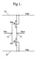
- CMOS inverter An embodiment of the present invention will be explained as applied to a CMOS inverter, however it will be understood that the invention may also be applied to other types of transistor circuit having components which are liable to gate-oxide dielectric breakdown and hot carrier degradation.
- CMOS inverter consisting of PMOS (M4) and NMOS (M1) transistors connected as shown.
- M4 PMOS
- M1 NMOS
- the input node 13 and output node 15 of the inverter take one of two logic states : logic 1 and logic 0. For example, if the input is at logic 1, then Vin, the voltage applied to input node 13 is set equal to Vdd. Similarly, at logic 0, Vin is set equal to Vss, Vss typically being 0V.
- substantially the entire voltage rail will be placed across M4 so that hot carrier degradation may occur during subsequent transitions from one logic state to another. Furthermore a similar voltage will be present across the gate-source of M1 and the gate-drain of M4 so that there is a risk of gate-oxide dielectric breakdown.
- FIG. 2 an inverter circuit.
- transistor M3 turns on and pulls Vout to Vss, i.e. Vout ⁇ Vss, which is logic 0.
- the gate-source voltage of transistor M6 (PMOS) is -5V, so M6 is turned on and pulls up node tgp 29 to Vdd.
- the gate-source voltage of M4 (PMOS) is zero and M4 is turned off.
- node tp 31 will be pulled down through the action of transistor M2 (PMOS) until tp reaches 5.5V.
- the gate-source voltage of M2 is below its threshold voltage and therefore it is turned off and hence tp stays at 5.5V.
- the operation of the device is similar upon the input making a transition from logic 1 to logic 0.
- the maximum gate-source, gate-drain and drain-source voltage of the transistors is limited to about 5.5V. In contrast to the conventional CMOS inverter wherein the maximum gate-source, gate-drain and drain-source voltages is 10V. In other words, the electrical stress is approximately halved, hence both hot carrier degradation and gate-oxide dielectric breakdown are significantly reduced.
- One disadvantage with the circuit described in Figure 2 is that some second-order effects, such as sub-threshold leakage current and diffusion-substrate junction leakage current may affect its performance.
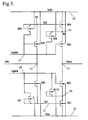
- additional transistors two PMOS M8, M9 and two NMOS M7, M10 are inserted into the inverter as shown in Figure 3 .
- the purpose of the additional transistors is to prevent the voltages tp, tgp, tn and tgn on nodes 31, 29, 23, 21 respectively from drifting beyond their normal operating points.
- transistor M9 PMOS
- node 31 remains at about 4.5V even when the leakage current in M4 is significant. Therefore, the drain-source voltage of M4 is equal to 5.5V instead of 10V, and the circuit continues to avoid hot carrier degradation and dielectric breakdown of its transistors.
- transistors M7-M10 are usually turned off during normal operation, they are only activated when any of the transistor leakage currents become significant. It will be understood by those skilled in the art that M7-M10 could be replaced by shottky or bipolar diodes or bipolar transistors or even high value resistors while maintaining the same protective function.
- any one of the resistors is selected to be low enough to clamp the voltage at the node but preferably to be as high as possible subject to the previous requirements as any excess current which passes through one of the transistors would represent a power wastage.
- M3-M6 M20, M21, M19, M18 operate to reduce the maximum drain-source voltage in order to avoid the hot-carrier degradation which would otherwise occur, while M16 and M17 operate to reduce the maximum gate-source voltage thereby preventing gate-oxide breakdown at M13 and M14.
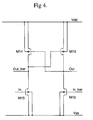
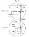
- FIG. 6 there appears a diagram of a typical electrode output driver circuit as might be used in the output stage of an electrical tissue stimulator device such as a cochlear implant prosthesis.
- the driver circuit has two switches 39, 41 and a current source formed by current minor comprising transistors M22, M23.
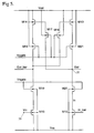
- the switching circuit of Figure 6 may be implemented as shown in Figure 7 where M24 and M25 have been used to reduce the maximum drain-source voltage, thereby avoiding hot-carrier degradation, while M27 has been incorporated to reduce the maximum gate-source voltage of M26 thereby avoiding gate-oxide dielectric breakdown.
Landscapes
- Physics & Mathematics (AREA)
- Engineering & Computer Science (AREA)
- Computer Hardware Design (AREA)
- Computing Systems (AREA)
- General Engineering & Computer Science (AREA)
- Mathematical Physics (AREA)
- Logic Circuits (AREA)
- Metal-Oxide And Bipolar Metal-Oxide Semiconductor Integrated Circuits (AREA)
- Semiconductor Integrated Circuits (AREA)
- Electronic Switches (AREA)
- Emergency Protection Circuit Devices (AREA)
Claims (16)
- Integrierte CMOS Schaltung, dargestellt auf einem Halbleitersubstrat und folgendes umfassend:einen ersten Transistor (M4) mit einem Gate,einen Eingangsknoten (13), verbunden zum Empfang eines Eingangssignals (Vin) mit einem Spannungsbereich, welcher sich von einem Referenzspannungspegel bis zu einem höheren Spannungspegel erstreckt,einen zweiten Transistor (M6) mit einem ersten Nicht-Gate-Anschluss, verbunden mit einem Gate des ersten Transistors (M4), einen zweiten Nicht-Gate-Anschluss, verbunden mit dem Eingangsknoten (13) zum Empfang des Eingangssignals (Vin), und ein Gate, verbunden mit einer Vorspannungsquelle (17), welche derart angeordnet ist, um einen Vorspannungspegel zwischen dem Referenzspannungspegel und dem höheren Spannungspegel zu erzeugen, womit verhindert wird dass eine maximale Spannung, die sich zwischen dem Gate-und einem Sourcebereich des ersten Transistors (M4) und dem Gate- und einem Drainbereich des ersten Transistors (M4) aufgebaut hat, den Spannungsbereich überschreitet, womit ein Ausfall des Gateoxids verhindert wird, undentweder:einen ersten Widerstand, angeschlossen zwischen dem Gate und dem ersten Nicht-Gate-Anschluss des zweiten Transistors (M6), wobei der erste Widerstand einen derartigen Wert aufweist, dass Drifterscheinungen am Knoten auf Grund von Leckagestrom des zweiten Transistors (M6) vermieden werden, odereine erste Halbleiteranordnung (M8), angeschlosssen zwischen dem Gate und dem ersten Nicht-Gate-Anschluss des zweiten Transistors (M6) in einer Anordnung, die Drifterscheinungen am Knoten auf Grund von Leckagestrom des zweiten Transistors (M6) verhindert.
- Integrierte CMOS Schaltung nach Anspruch 1, worin die erste Halbleiteranordnung (M8) ein Element aus der Gruppe Schottky-Diode, CMOS-Transistor, Bipolar-Diode oder Bipolar-Transistor umfasst.
- Integrierte CMOS Schaltung nach Anspruch 1 oder 2, worin der erste Nicht-Gate-Anschluss des zweiten Transistors (M6) ein Sourcebereich ist und der zweite Nicht-Gate-Anschluss des zweiten Transistors (M6) ein Drainbereich ist.
- Integrierte CMOS Schaltung nach einem der vorhergehenden Ansprüche, wobei weiterhin folgendes umfasst ist:ein dritter Transistor (M2) mit einem Gate, verbunden mit der Vorspannungsquelle (17), ein erster Nicht-Gate-Anschluss, verbunden mit einem Nicht-Gate-Anschluss des ersten Transistors (M4), und ein zweiter Anschluss, verbunden mit einem Ausgangsanschluss (15),wobei der dritte Transistor (M2) unter Vorspannung steht um zu verhindern, dass die maximale Spannung, welche sich zwischen dem Sourcebereich des ersten Transistors (M4) und dem Drainbereich des ersten Transistors (M4) aufgebaut hat, den Spannungsbereich übersteigt, womit verhindert wird, dass sich eine Trägerzersetzung des ersten Transistors (M4) unter Wärmeeinfluß ergibt.
- Integrierte CMOS Schaltung nach Anspruch 4, wobei, falls die erste Halbleiteranordnung (M8) angeschlossen ist, eine zweite Halbleiteranordnung (M9) verbunden ist mit dem Gatebereich und dem ersten Nicht-Gate-Anschluss des dritten Transistors (M2), in einer Anordnung, welche Drifterscheinungen am Knoten auf Grund von Leckagestrom des dritten Transistors (M2) verhindert.
- Integrierte CMOS Schaltung nach Anspruch 5, worin die zweite Halbleiteranordnung (M9) ein Element aus der Gruppe Schottky-Diode, CMOS-Transistor, Bipolar-Diode oder Bipolar-Transistor umfasst.
- Integrierte CMOS Schaltung nach Anspruch 4, wobei, falls der erste Widerstand angeschlossen ist, ein zweiter Widerstand zwischen dem Gatebereich und dem ersten Nicht-Gate-Anschluss des dritten Transistors (M2) angeschlossen ist, wobei der zweite Widerstand einen Wert aufweist, der derart ausgewählt ist um Drifterscheinungen am Knoten auf Grund von Leckagestrom des dritten Transistors (M2) zu verhindern.
- Integrierte CMOS Schaltung nach Anspruch 1, welche in einer CMOS-Inverter-Schaltung integriert ist, angeschlossen zwischen einer ersten Energieversorgungs-Spannungsquelle (Vdd) und einer zweiten Energieversorgungs-Spannungsquelle (Vss), wobei die zweite Energieversorgungs-Spannungsquelle (Vss) einen Spannungspegel aufweist, der kleiner ist als der der ersten Energieversorgungs-Spannungsquelle (Vdd), wobei
ein Nicht-Gate-Anschluss des ersten Transistors (M4) mit einer der ersten oder der zweiten Energieversorgungs-Spannungsquellen verbunden ist,
wobei die Schaltung weiterhin aufweist:einen dritten Transistor (M1), einen Nicht-Gate-Anschluss des dritten Transistors (M1), verbunden mit der anderen der Energieversorgungs-Spannungsquellen und ein Gate des dritten Transistors (M1), welches mit dem Eingangsknoten (13) verbunden ist,worin Drainanschlüsse des ersten und des dritten Transistors (M4,M1) miteinander verbunden sind und damit einen Ausgangsknoten (17) darstellen, und
worin im Betrieb der Spannungsbereich des Eingangssignals (Vin) sich zwischen den Spannungspegeln der ersten und der zweiten Energieversorgungs-Spannungsquelle (Vdd,Vss) erstreckt. - Integrierte CMOS Schaltung nach Anspruch 8, die weiterhin aufweist:einen vierten Transistor (M5) mit einem ersten Nicht-Gate-Anschluss, angeschlossen an dem Gate des dritten Transistors (M1), einen zweiten Nicht-Gate-Anschluss, verbunden mit dem Eingangsknoten (13) und ein Gate, verbunden mit der Vorspannungsquelle (19), womit ein Ausfall des GateOxids des dritten Transistors (M1) vermieden wird.
- Integrierte CMOS Schaltung nach Anspruch 9, welcher weiterhin aufweist:einen fünften Transistor (M2) mit einem Gate, verbunden mit der Vorspannungsquelle (17), einen ersten Nicht-Gate-Anschluss, verbunden mit einem Nicht-Gate-Anschluss des ersten Transistors (M4) und einen zweiten Nicht-Gate-Anschluss, verbunden mit dem Ausgangsknoten (15), womit vermieden wird, dass der dritte Transistor (M4) einer Trägerzersetzung unter Wärmeeinfluß unterworfen ist.
- Integrierte CMOS Schaltung nach Anspruch 10, welche weiterhin aufweist:einen sechsten Transistor (M3) mit einem Gate, verbunden mit der Vorspannungsquelle (19), einen ersten Nicht-Gate-Anschluss, verbunden mit einem Nicht-Gate-Anschluss des dritten Transistors (M1) und einen zweiten Nicht-Gate-Anschluss, verbunden mit dem Ausgangsknoten (15), womit eine Trägerzersetzung des dritten Transistors (M1) unter Wärmeeinfluß vermieden wird.
- Integrierte CMOS Schaltung nach Anspruch 11, wobei, falls die erste Halbleiteranordnung (M8) angeschlossen ist, weiterhin umfasst ist:eine weitere Halbleiteranordnung (M7,M9,M10), angeschlossen zwischen dem Gate- und dem Sourcebereich von einem, dem vierten, fünften oder sechsten Transistor (M2,M3,M5), womit eine Drift am Knotenpunkt auf Grund des Leckagestroms eines der vierten, fünften oder sechsten Transistoren (M2,M3,M5) verhindert wird.
- Integrierte CMOS Schaltung nach Anspruch 12, worin die weitere Halbleiteranordnung (M7,M9,M10) ein Element aus der Gruppe Schottky-Diode, CMOS-Transistor, Bipolar-Diode oder Bipolar-Transistor umfasst.
- Integrierte CMOS Schaltung nach Anspruch 11, wobei, falls der erste Widerstand angeschlossen ist, weiterhin umfasst ist:ein weiterer Widerstand, verbunden mit dem Gate- und Sourcebereich von irgend einem, dem vierten, fünften oder sechsten Transistor (M2,M3,M5), womit ein Driften auf Grund des Leckagestroms von einem der vierten, fünften oder sechsten Transistoren (M2,M3,M5) am Knoten vermieden wird.
- Integrierte CMOS Schaltung nach einem der Ansprüche 1 bis 7, worin die Schaltung weiterhin ausgelegt ist als eine Pegelübersetzungsschaltung.
- Integrierte CMOS Schaltung nach einem der Ansprüche 1 bis 7, worin die Schaltung weiterhin ausgelegt ist als eine schaltbare Stromquelle.
Applications Claiming Priority (1)
| Application Number | Priority Date | Filing Date | Title |
|---|---|---|---|
| PCT/AU1999/000519 WO2001003301A1 (en) | 1999-06-29 | 1999-06-29 | High voltage protection circuit on standard cmos process |
Publications (3)
| Publication Number | Publication Date |
|---|---|
| EP1190487A1 EP1190487A1 (de) | 2002-03-27 |
| EP1190487A4 EP1190487A4 (de) | 2003-07-16 |
| EP1190487B1 true EP1190487B1 (de) | 2008-03-26 |
Family
ID=3764586
Family Applications (1)
| Application Number | Title | Priority Date | Filing Date |
|---|---|---|---|
| EP99928892A Expired - Lifetime EP1190487B1 (de) | 1999-06-29 | 1999-06-29 | Schutzschaltung gegen hochspannung für standard cmos prozess |
Country Status (8)
| Country | Link |
|---|---|
| US (1) | US6377075B1 (de) |
| EP (1) | EP1190487B1 (de) |
| JP (1) | JP4763192B2 (de) |
| AT (1) | ATE390761T1 (de) |
| AU (1) | AU761220B2 (de) |
| CA (1) | CA2377896A1 (de) |
| DE (1) | DE69938434T2 (de) |
| WO (1) | WO2001003301A1 (de) |
Families Citing this family (24)
| Publication number | Priority date | Publication date | Assignee | Title |
|---|---|---|---|---|
| US7199612B2 (en) * | 2002-08-12 | 2007-04-03 | Broadcom Corporation | Method and circuit for reducing HCI stress |
| US7068091B1 (en) * | 2003-02-27 | 2006-06-27 | Cypress Semiconductor Corporation | Voltage translator circuit formed using low voltage transistors |
| US7274209B1 (en) | 2003-06-26 | 2007-09-25 | Cypress Semiconductor Corporation | Low voltage to high voltage signal level translator with improved performance |
| EP1492232A1 (de) | 2003-06-27 | 2004-12-29 | Dialog Semiconductor GmbH | Komparator mit Hochspannungseingängen in einem erweiterten CMOS-Prozess für Hochspannungspegel |
| US7205830B2 (en) * | 2005-01-04 | 2007-04-17 | International Business Machines Corporation | Analog MOS circuits having reduced voltage stress |
| US7332956B2 (en) * | 2005-10-27 | 2008-02-19 | International Business Machines Corporation | Method to avoid device stressing |
| EP2011236B1 (de) * | 2006-04-12 | 2011-02-02 | Nxp B.V. | Elektronische schaltung |
| JP4991436B2 (ja) * | 2007-08-02 | 2012-08-01 | キヤノン株式会社 | 撮像装置及び撮像システム |
| US7694243B2 (en) * | 2007-12-27 | 2010-04-06 | International Business Machines Corporation | Avoiding device stressing |
| US8154270B2 (en) * | 2009-02-13 | 2012-04-10 | Standard Microsystems Corporation | Power-up control for very low-power systems |
| CN102782806A (zh) | 2010-03-04 | 2012-11-14 | 株式会社安川电机 | 工作台装置 |
| US9086709B2 (en) | 2013-05-28 | 2015-07-21 | Newlans, Inc. | Apparatus and methods for variable capacitor arrays |
| US9570222B2 (en) | 2013-05-28 | 2017-02-14 | Tdk Corporation | Vector inductor having multiple mutually coupled metalization layers providing high quality factor |
| US9461610B2 (en) * | 2014-12-03 | 2016-10-04 | Tdk Corporation | Apparatus and methods for high voltage variable capacitors |
| US9735752B2 (en) | 2014-12-03 | 2017-08-15 | Tdk Corporation | Apparatus and methods for tunable filters |
| US9671812B2 (en) | 2014-12-17 | 2017-06-06 | Tdk Corporation | Apparatus and methods for temperature compensation of variable capacitors |
| US9362882B1 (en) | 2015-01-23 | 2016-06-07 | Tdk Corporation | Apparatus and methods for segmented variable capacitor arrays |
| US10382002B2 (en) | 2015-03-27 | 2019-08-13 | Tdk Corporation | Apparatus and methods for tunable phase networks |
| US9680426B2 (en) | 2015-03-27 | 2017-06-13 | Tdk Corporation | Power amplifiers with tunable notches |
| US10042376B2 (en) | 2015-03-30 | 2018-08-07 | Tdk Corporation | MOS capacitors for variable capacitor arrays and methods of forming the same |
| US9595942B2 (en) | 2015-03-30 | 2017-03-14 | Tdk Corporation | MOS capacitors with interleaved fingers and methods of forming the same |
| US10073482B2 (en) | 2015-03-30 | 2018-09-11 | Tdk Corporation | Apparatus and methods for MOS capacitor structures for variable capacitor arrays |
| US9973155B2 (en) | 2015-07-09 | 2018-05-15 | Tdk Corporation | Apparatus and methods for tunable power amplifiers |
| WO2021171482A1 (ja) | 2020-02-27 | 2021-09-02 | 株式会社ソシオネクスト | 出力回路、送信回路及び半導体集積回路 |
Family Cites Families (18)
| Publication number | Priority date | Publication date | Assignee | Title |
|---|---|---|---|---|
| JPS54140481A (en) * | 1978-04-21 | 1979-10-31 | Nec Corp | Semiconductor device |
| JPS577969A (en) * | 1980-06-18 | 1982-01-16 | Toshiba Corp | Semiconductor integrated circuit |
| US4508978A (en) * | 1982-09-16 | 1985-04-02 | Texas Instruments Incorporated | Reduction of gate oxide breakdown for booted nodes in MOS integrated circuits |
| JPS6187357A (ja) * | 1984-09-18 | 1986-05-02 | Sanyo Electric Co Ltd | 半導体集積回路装置 |
| JPH0738583B2 (ja) * | 1985-01-26 | 1995-04-26 | 株式会社東芝 | 半導体集積回路 |
| JPS61276249A (ja) * | 1985-05-30 | 1986-12-06 | Toshiba Corp | 入力保護回路 |
| JPH0536919A (ja) * | 1991-07-29 | 1993-02-12 | Nec Corp | 半導体集積回路装置 |
| US5136190A (en) * | 1991-08-07 | 1992-08-04 | Micron Technology, Inc. | CMOS voltage level translator circuit |
| KR940009696B1 (ko) * | 1991-10-08 | 1994-10-15 | 현대전자산업주식회사 | 열 캐리어 방지 회로 |
| JP3197920B2 (ja) * | 1991-10-31 | 2001-08-13 | 富士通株式会社 | 半導体集積回路 |
| JP3554353B2 (ja) * | 1994-02-14 | 2004-08-18 | シーメンス アクチエンゲゼルシヤフト | 電界効果トランジスタの保護装置 |
| US5440249A (en) * | 1994-05-03 | 1995-08-08 | Motorola, Inc. | Voltage level translator circuit with cascoded output transistors |
| US5633602A (en) * | 1995-09-14 | 1997-05-27 | Ncr Corporation | Low voltage CMOS to low voltage PECL converter |
| US5726589A (en) * | 1995-11-01 | 1998-03-10 | International Business Machines Corporation | Off-chip driver circuit with reduced hot-electron degradation |
| US5892371A (en) * | 1996-02-12 | 1999-04-06 | Advanced Micro Devices, Inc. | Gate oxide voltage limiting devices for digital circuits |
| JP2993462B2 (ja) * | 1997-04-18 | 1999-12-20 | 日本電気株式会社 | 出力バッファ回路 |
| KR100261558B1 (ko) * | 1997-07-15 | 2000-07-15 | 김영환 | 씨모스 디지탈 레벨 시프트 회로 |
| US6130557A (en) * | 1999-04-26 | 2000-10-10 | Ati Technologies, Inc. | Three level pre-buffer voltage level shifting circuit and method |
-
1999
- 1999-06-29 CA CA002377896A patent/CA2377896A1/en not_active Abandoned
- 1999-06-29 JP JP2001508599A patent/JP4763192B2/ja not_active Expired - Fee Related
- 1999-06-29 DE DE69938434T patent/DE69938434T2/de not_active Expired - Lifetime
- 1999-06-29 WO PCT/AU1999/000519 patent/WO2001003301A1/en not_active Ceased
- 1999-06-29 AT AT99928892T patent/ATE390761T1/de active
- 1999-06-29 AU AU45910/99A patent/AU761220B2/en not_active Ceased
- 1999-06-29 EP EP99928892A patent/EP1190487B1/de not_active Expired - Lifetime
- 1999-11-04 US US09/428,968 patent/US6377075B1/en not_active Expired - Lifetime
Also Published As
| Publication number | Publication date |
|---|---|
| JP2003504860A (ja) | 2003-02-04 |
| DE69938434D1 (de) | 2008-05-08 |
| AU4591099A (en) | 2001-01-22 |
| DE69938434T2 (de) | 2008-09-18 |
| WO2001003301A1 (en) | 2001-01-11 |
| AU761220B2 (en) | 2003-05-29 |
| CA2377896A1 (en) | 2001-01-11 |
| EP1190487A1 (de) | 2002-03-27 |
| ATE390761T1 (de) | 2008-04-15 |
| US6377075B1 (en) | 2002-04-23 |
| EP1190487A4 (de) | 2003-07-16 |
| JP4763192B2 (ja) | 2011-08-31 |
Similar Documents
| Publication | Publication Date | Title |
|---|---|---|
| EP1190487B1 (de) | Schutzschaltung gegen hochspannung für standard cmos prozess | |
| US5969542A (en) | High speed gate oxide protected level shifter | |
| US6803801B2 (en) | CMOS level shifters using native devices | |
| JP3118071B2 (ja) | レベル変換回路 | |
| US7969191B2 (en) | Low-swing CMOS input circuit | |
| JP3916694B2 (ja) | 耐高電圧cmos入力/出力パッド回路 | |
| US7102410B2 (en) | High voltage level converter using low voltage devices | |
| KR20010071855A (ko) | 고전압 레벨 허용 트랜지스터 회로 | |
| CN109327218B (zh) | 一种电平移位电路和集成电路芯片 | |
| US6842063B2 (en) | Analog switch circuit | |
| JPS6323417A (ja) | Cmosパワ−オンリセツト回路 | |
| US5479116A (en) | Level conversion circuits for converting a digital input signal varying between first and second voltage levels to a digital output signal varying between first and third voltage levels | |
| US6239630B1 (en) | CMOS-compatible power-on reset circuit | |
| KR100334365B1 (ko) | 시모스 입력 버퍼 보호 회로 | |
| US20050218935A1 (en) | Data output circuit with improved overvoltage/surge protection | |
| KR19990083514A (ko) | Cmos기준전압발생기 | |
| JPH11355116A (ja) | Cmos出力バッファ保護回路を有する集積回路 | |
| JP2002043924A (ja) | 半導体集積回路装置の入力インターフェイス回路 | |
| US20040061524A1 (en) | Digital electronic circuit for translating high voltage levels to low voltage levels | |
| US6452827B1 (en) | I/O circuit of semiconductor integrated device | |
| WO2000001070A1 (en) | An 'on-chip' higher-to-lower voltage input stage | |
| JPH0563540A (ja) | 入力回路 | |
| US20250141442A1 (en) | High voltage tolerant bootstrap switch | |
| JP3722741B2 (ja) | 電圧供給回路 | |
| EP1472788A2 (de) | Spannungsbegrenzende halbleiter-durchgangsgatterschaltung |
Legal Events
| Date | Code | Title | Description |
|---|---|---|---|
| PUAI | Public reference made under article 153(3) epc to a published international application that has entered the european phase |
Free format text: ORIGINAL CODE: 0009012 |
|
| 17P | Request for examination filed |
Effective date: 20020109 |
|
| AK | Designated contracting states |
Kind code of ref document: A1 Designated state(s): AT DE FR GB |
|
| A4 | Supplementary search report drawn up and despatched |
Effective date: 20030604 |
|
| RIC1 | Information provided on ipc code assigned before grant |
Ipc: 7H 03K 19/003 B Ipc: 7H 01L 27/02 B Ipc: 7H 01L 27/06 B Ipc: 7H 03K 17/10 B Ipc: 7H 03K 19/0948 A |
|
| 17Q | First examination report despatched |
Effective date: 20040211 |
|
| GRAP | Despatch of communication of intention to grant a patent |
Free format text: ORIGINAL CODE: EPIDOSNIGR1 |
|
| GRAS | Grant fee paid |
Free format text: ORIGINAL CODE: EPIDOSNIGR3 |
|
| GRAA | (expected) grant |
Free format text: ORIGINAL CODE: 0009210 |
|
| AK | Designated contracting states |
Kind code of ref document: B1 Designated state(s): AT DE FR GB |
|
| REG | Reference to a national code |
Ref country code: GB Ref legal event code: FG4D |
|
| REF | Corresponds to: |
Ref document number: 69938434 Country of ref document: DE Date of ref document: 20080508 Kind code of ref document: P |
|
| PGFP | Annual fee paid to national office [announced via postgrant information from national office to epo] |
Ref country code: FR Payment date: 20080331 Year of fee payment: 10 |
|
| ET | Fr: translation filed | ||
| PGFP | Annual fee paid to national office [announced via postgrant information from national office to epo] |
Ref country code: GB Payment date: 20080401 Year of fee payment: 10 |
|
| PLBE | No opposition filed within time limit |
Free format text: ORIGINAL CODE: 0009261 |
|
| STAA | Information on the status of an ep patent application or granted ep patent |
Free format text: STATUS: NO OPPOSITION FILED WITHIN TIME LIMIT |
|
| 26N | No opposition filed |
Effective date: 20081230 |
|
| GBPC | Gb: european patent ceased through non-payment of renewal fee |
Effective date: 20090629 |
|
| PG25 | Lapsed in a contracting state [announced via postgrant information from national office to epo] |
Ref country code: GB Free format text: LAPSE BECAUSE OF NON-PAYMENT OF DUE FEES Effective date: 20090629 |
|
| REG | Reference to a national code |
Ref country code: FR Ref legal event code: ST Effective date: 20120309 |
|
| PG25 | Lapsed in a contracting state [announced via postgrant information from national office to epo] |
Ref country code: FR Free format text: LAPSE BECAUSE OF NON-PAYMENT OF DUE FEES Effective date: 20090630 |
|
| PGFP | Annual fee paid to national office [announced via postgrant information from national office to epo] |
Ref country code: DE Payment date: 20120627 Year of fee payment: 14 |
|
| PGFP | Annual fee paid to national office [announced via postgrant information from national office to epo] |
Ref country code: AT Payment date: 20120529 Year of fee payment: 14 |
|
| REG | Reference to a national code |
Ref country code: AT Ref legal event code: MM01 Ref document number: 390761 Country of ref document: AT Kind code of ref document: T Effective date: 20130629 |
|
| REG | Reference to a national code |
Ref country code: DE Ref legal event code: R119 Ref document number: 69938434 Country of ref document: DE Effective date: 20140101 |
|
| PG25 | Lapsed in a contracting state [announced via postgrant information from national office to epo] |
Ref country code: DE Free format text: LAPSE BECAUSE OF NON-PAYMENT OF DUE FEES Effective date: 20140101 |
|
| PG25 | Lapsed in a contracting state [announced via postgrant information from national office to epo] |
Ref country code: AT Free format text: LAPSE BECAUSE OF NON-PAYMENT OF DUE FEES Effective date: 20130629 |