EP1159629B1 - Efficient parallel testing of integrated circuit devices using a known good device to generate expected responses - Google Patents
Efficient parallel testing of integrated circuit devices using a known good device to generate expected responses Download PDFInfo
- Publication number
- EP1159629B1 EP1159629B1 EP00910351A EP00910351A EP1159629B1 EP 1159629 B1 EP1159629 B1 EP 1159629B1 EP 00910351 A EP00910351 A EP 00910351A EP 00910351 A EP00910351 A EP 00910351A EP 1159629 B1 EP1159629 B1 EP 1159629B1
- Authority
- EP
- European Patent Office
- Prior art keywords
- tester
- reference device
- integrated circuit
- read
- data
- Prior art date
- Legal status (The legal status is an assumption and is not a legal conclusion. Google has not performed a legal analysis and makes no representation as to the accuracy of the status listed.)
- Expired - Lifetime
Links
- 238000012360 testing method Methods 0.000 title claims description 69
- 230000004044 response Effects 0.000 title claims description 19
- 239000000523 sample Substances 0.000 claims description 20
- 238000004891 communication Methods 0.000 claims description 7
- 238000012544 monitoring process Methods 0.000 claims description 4
- 101100117775 Arabidopsis thaliana DUT gene Proteins 0.000 claims 6
- 101150091805 DUT1 gene Proteins 0.000 claims 6
- 238000010586 diagram Methods 0.000 description 7
- 239000004065 semiconductor Substances 0.000 description 4
- 230000006870 function Effects 0.000 description 3
- 238000004519 manufacturing process Methods 0.000 description 3
- 238000000034 method Methods 0.000 description 3
- 230000009471 action Effects 0.000 description 1
- 238000013459 approach Methods 0.000 description 1
- 230000006399 behavior Effects 0.000 description 1
- 230000008901 benefit Effects 0.000 description 1
- 230000008859 change Effects 0.000 description 1
- 230000006835 compression Effects 0.000 description 1
- 238000007906 compression Methods 0.000 description 1
- 239000000470 constituent Substances 0.000 description 1
- 230000008878 coupling Effects 0.000 description 1
- 238000010168 coupling process Methods 0.000 description 1
- 238000005859 coupling reaction Methods 0.000 description 1
- 230000007547 defect Effects 0.000 description 1
- 230000001419 dependent effect Effects 0.000 description 1
- 230000001747 exhibiting effect Effects 0.000 description 1
- 230000002349 favourable effect Effects 0.000 description 1
- 238000013100 final test Methods 0.000 description 1
- 230000003278 mimic effect Effects 0.000 description 1
- 238000012986 modification Methods 0.000 description 1
- 230000004048 modification Effects 0.000 description 1
- 230000008569 process Effects 0.000 description 1
- 230000001737 promoting effect Effects 0.000 description 1
- 230000001902 propagating effect Effects 0.000 description 1
- 230000007704 transition Effects 0.000 description 1
- 239000013598 vector Substances 0.000 description 1
Images


Classifications
-
- G—PHYSICS
- G01—MEASURING; TESTING
- G01R—MEASURING ELECTRIC VARIABLES; MEASURING MAGNETIC VARIABLES
- G01R31/00—Arrangements for testing electric properties; Arrangements for locating electric faults; Arrangements for electrical testing characterised by what is being tested not provided for elsewhere
- G01R31/28—Testing of electronic circuits, e.g. by signal tracer
- G01R31/317—Testing of digital circuits
- G01R31/3181—Functional testing
- G01R31/319—Tester hardware, i.e. output processing circuits
- G01R31/3193—Tester hardware, i.e. output processing circuits with comparison between actual response and known fault free response
-
- G—PHYSICS
- G01—MEASURING; TESTING
- G01R—MEASURING ELECTRIC VARIABLES; MEASURING MAGNETIC VARIABLES
- G01R31/00—Arrangements for testing electric properties; Arrangements for locating electric faults; Arrangements for electrical testing characterised by what is being tested not provided for elsewhere
- G01R31/28—Testing of electronic circuits, e.g. by signal tracer
- G01R31/317—Testing of digital circuits
- G01R31/3181—Functional testing
- G01R31/319—Tester hardware, i.e. output processing circuits
- G01R31/31903—Tester hardware, i.e. output processing circuits tester configuration
- G01R31/31905—Interface with the device under test [DUT], e.g. arrangements between the test head and the DUT, mechanical aspects, fixture
Definitions
- This invention is related to the testing of integrated circuit devices using a semiconductor tester, and more particularly to testing a number of devices in parallel.
- Integrated circuit (IC) devices are an important part of almost every modern electronic or computer system. To reduce the manufacturing cost of such systems, the manufacturer expects each constituent IC device to be virtually free of defects and to perform according to its specifications. Thus, it is not unusual to expect that every IC device is subjected to rigorous testing prior to being shipped to the system manufacturer.
- a memory device may be tested using an automated semiconductor tester.
- Figure 5 shows such a tester 502 having a number (N) of channels for parallel testing of a number of devices under test 518 (DUTs.)
- the DUT 518 may have a memory cell array and built-in self test (BIST) circuitry.
- the tester 502 normally executes a test program and in response generates data and addresses which define a test sequence 506 engineered for testing the particular DUTs.
- the data and addresses on each channel of the tester are fed to a respective DUT, so that a number of DUTs, corresponding to the number of channels, may be tested simultaneously.
- a probe card (not shown) receiving all N channels delivers address and write data of the test sequence to locations in the N different DUTs simultaneously.
- the tester 502 can read the data from the locations in the DUTs for comparison with expected data. This may occur while the DUTs are still part of the semiconductor wafer 516 as shown. The results of the comparison help determine whether some portion of the device is functioning improperly, for example whether a particular bit read from a location in the memory device is in error.
- the tester performs the above read and write cycles many times with the same or different data patterns to verify as many locations of the DUTs as possible given time and budget constraints.
- a larger tester may be built with more channels.
- the tester 502 is a complex and high speed machine, requiring much time and expense to modify or improve.
- a single channel of a modem tester may comprise between 50 to 100 signal wires, such that increasing the number of channels between the tester and the probe card will make it physically impractical to connect all of the signal wires to the probe card. Therefore, a more efficient solution for increasing the throughput of an IC test system is needed.
- Patent Abstracts of Japan, Vol. 018, No. 241 (P-1733), 09.05.94 & JP 06027195 A disclose a test system designed to test several integrated circuits on a board. Using time division multiplexing, test pulses generated by a pulse generator are written to the known-good device (KGD) and all of the integrated circuits on board. Also in this time-division multiplexing the test answer signals of the integrated circuits are compared to the answer signals of the KGD.
- KGD known-good device
- IBM Technical Disclosure Bulletin, Vol. 39, No. 07, July 96, p. 243-244 discloses a tester for simultaneously testing a plurality of memory product cards, wherein the plurality of memory product cards is interfaced to the tester via a test adapter. A corresponding plurality of product interface cards is provided on the test adapter each connecting to one of the memory product cards. The product interface cards perform comparison of test results for each memory product card and store error information.
- the invention is defined in claim 1.
- Claim 1 provides a system having a tester, a known good device, a channel coupled between the tester and the known good device for data communication between the known good device and the tester, and interface circuitry for monitoring the channel.
- the tester writes data as part of a test sequence to locations in the known good device and subsequently reads data from corresponding locations in each of a number of devices under test (DUTs).
- the interface circuitry monitors the channel while the tester is writing and reading to and from the locations in the known good device and in response performs a write or read from corresponding locations in the DUTs.
- the interface circuitry makes comparisons between data from the known good device and data from the DUTs.
- results of the test may then be communicated to the tester.
- the tester may itself issue commands to the test circuit to configure the local action.
- the interface circuits includes logic means for detecting these commands, and for managing local test functions. The latter may include propagating writes to one or more connected DUTs in parallel, in response to having snooped writes to the KGD.
- the test circuit may also manage the memory circuitry as needed by, for instance, applying refresh cycles.
- an embodiment of the invention provides for more efficient testing of a number of similar, and preferably identical, IC devices in parallel without altering the test program or the conventional tester.
- each channel is still testing a single device, in this case the known good device (KGD), according to the conventional test sequence.
- the tester-DUT interface circuitry monitors the channel while the tester is writing data as part of a test pattern to locations in the known good device.
- the interface circuitry then writes the data to corresponding locations into 1 to M DUTs.
- the interface circuitry detects such a read and itself reads DUT data from corresponding locations in the DUTs.
- the tester does not have to explicitly produce expected data for the read comparison, which contributes to overall faster testing.
- a comparison is then made by the interface circuitry using the DUT data read from the DUTs to generate error information.
- the tester or system controller may then read the error information provided by the interface circuitry, according to a manufacturing fabrication flow process.
- Figure 1 illustrates a block diagram of a test system 102 according to an embodiment of the invention.
- the tester may be the HP83000 model by Hewlett Packard, Inc., a tester which complies with the popular Direct Rambus Dynamic Random Access Memory (DRDRAM) memory device specification.
- DRAM Direct Rambus Dynamic Random Access Memory
- a DUT may itself be a memory chip, or it may be an arbitrary semiconductor device including a memory portion thereof.
- a known good device (KGD) 112 is communicatively coupled to the tester 104 via the channel 108.
- the KGD may be an actual specimen of a DUT which has undergone a sufficient amount of testing to ensure it is a good device with no errors.
- the KGD may be hardware that simulates the behavior of an actual DUT under error free conditions.
- the interface circuitry 116 comprises a number of substantially identical tester-DUT interface blocks 120 1 , 120 2 . . . . (120 i ). One or more of these may be implemented as a separate application specific integrated circuit (ASIC) chip. Alternatively, the functionality described below for each block 120 i may be separated among several chips. Although sixteen blocks are shown in Figure 1 , in general a fewer or greater number M may be used, considering the number of DUTs to test and the load capabilities of the channel 108. Yet other circuit configurations for interfacing the DUTs to the channel 108 may be developed by one of ordinary skill in the art in view of the functionality described in this disclosure.
- ASIC application specific integrated circuit
- the interface circuitry 116 may also be configured to compare KGD data and timing with DUT data and timing read by the interface.
- the KGD data and timing may be obtained by the interface circuitry 116 snooping the channel 108 while the tester is reading from and writing to the KGD.
- Figure 2 shows a block diagram of a portion of the tester-DUT interface block 120 i that constitutes the interface circuitry 116 according to an embodiment of the invention.
- up to M DUT ports may be provided, each for interfacing a single DUT.
- the DUT ports 204A and 204B write to and read from their respective DUTs in response to address and data received from a channel port 208 and in response to other control indications from address and instruction decode logic 212. After the address, data, and control (e.g., Read/Write) information are captured from the channel 108 by the channel port 208, they are fed to the address and instruction decode logic 212.
- address, data, and control e.g., Read/Write
- the logic 212 monitors read and write transactions in the channel 108 by decoding the address, data, R/W signal, and control information received from the channel port 208 to determine the next operation of the logic 212 (read to or write from the DUTs).
- Each block 120 i and more particularly the address and decode logic 212, has knowledge of the address range of the known good device 112 (see Figure 1 ), so that when the tester 104 is writing to or reading from the known good device 112, the block 120 i can invoke the same read and write transactions with its respective DUTs. Additionally, the decode logic 212 is aware of the address range of a number of control and status registers (CSRs) and of the DUT ports.
- CSRs control and status registers
- the address range may include control information used to set appropriate bits in the CSRs 220 to initialize the block 120 i and to place the block 120 i in different modes of operation.
- Each individual block 120 i and hence the entire interface circuitry 116, may be placed into different modes of operation by writing to and reading from the CSRs 220.
- each of the DUT ports should be assigned a different address range.
- An address mapper 216 is provided to map the address of a location in the KGD to corresponding locations in the DUTs. For instance, if the address range of the KGD is 0-64M, the address range for DUT port 1 could be 64-128M, the address range for DUT port 2 could be 128M-196M, and so on. This also allows the DUT ports to share the same address lines in the block 120 i , yielding a more efficient circuit configuration for each block.
- a comparator circuit 224 is provided for performing a comparison using DUT data which has been read from its respective DUT.
- each of the comparators receives two sixteen bit values, one being read data from a respective DUT and the other being read data from the KGD received from the channel port 208.
- Clock resynchronization and pipeline registers may be used to align data at each comparator 224.
- the internal data bus 266 is 16 bits wide in this example, a wide range of alternative widths for the data bus 266 and address bus 268 may be used.
- Each comparator 224 generates raw error data being the result of bit-wise XOR operations performed upon a DUT data value and a KGD data value.
- This raw error data may be stored either in the CSRs 220, or in a memory (not shown) separate from each block 120 i .
- the tester 104 may then access this memory at a later time, through the channel 108 or through an alternative path, to read the raw error data.
- a compression scheme may be implemented where, for instance, a single error bit is generated for each respective comparison. This gives an indication that an error has occurred in a given group of bits of a given DUT, without specifying which bit among the many in that group is actually in error. This allows, for instance, a channel 108 having a data bus being 16 bits wide to deliver error information back to the tester for up to 16 DUTs simultaneously.
- These flags may indicate errors in a particular DUT or in a particular range of addresses. They may be read by the tester 104 following completion of the test sequence to quickly determine if any errors were encountered. The tester 104 can then optionally test the address range or DUT that is in error in a more detailed manner to determine which specific bit(s) are in error.
- a DUT clocking signal 256 is used by the DUT ports to synchronize the writing to and reading from the respective DUTs, and to resynchronize the data from the channel port 208 to a DUT port.
- the signal 256 may be provided by a clock generator 232 comprising either a phase-locked or delay-locked loop.
- the clock generator 232 runs based on a clock signal received from the tester 104.
- the clock generator 232 also provides a clock control signal 258 for varying the phase of the clock fed to each DUT with respect to the clock signal received from the tester 104. This may be used for clock margin testing of each DUT.
- the DUT clocking signal 256 and control signal 258 may be varied by programming the CSRs 220.
- the decode logic 212 in response to detecting a read or write to a particular address range signals a state machine 228 to transition into the appropriate state as shown in the bubble diagram of Figure 3 .
- Operation of each block 120 i as well as the overall test system 102 may be explained in conjunction with this state diagram. Operation normally begins with the tester 104 initializing the interface circuitry 116, e.g., by initializing each interface block 120 i , by sending a write transaction over the channel 108 directed at the address range of the CSRs 220.
- a machine other than the tester 104 can perform the initialization of the CSRs 220 and of each block 120 i through an auxiliary port (not shown) that may be coupled to the CSRs 220.
- the block 120 ⁇ After the block 120 ⁇ has been initialized or reset, it is in the Idle state 302 as indicated in Figure 3 . While Idle, however, the block 120 i will normally be reading its CSRs 220 regularly. Before the tester 104 starts to execute its test sequence and write to the known good device 112, the tester 104 writes to the CSRs 220 requesting a change in the mode of operation to the Monitor state 304. The state machine 228 responds by entering the Monitor state 304. In that state, the block 120 i monitors the channel 108 while the tester 104 is writing data to the KGD 112.
- the block 120 i In response to a write transaction detected by the decode logic 212, the block 120 i enters the Mimic Write state 308 in which the KGD bound data is captured from the channel 108 and is written to corresponding locations in each DUT. Write transactions continue to be mimicked in this way until the tester 104 enters a read cycle.
- the tester 104 will normally read from locations in the KGD 112 to which data has been previously written.
- the decode logic 212 detects such read transactions and signals the state machine 228 to enter the Mimic Read state 312. In this state, the block 120 i mimics the tester's read transaction on all of the DUTs and performs comparisons to determine errors in the DUTs.
- a KGD data value expected value
- the decode logic 212 initiates a read from corresponding locations in the DUTs which brings DUT data values into each comparator 224, one from each DUT.
- a comparison may then be made between the read data value from the KGD and the read data value from a corresponding DUT. Since the KGD data value was provided by a "good" device, the KGD data value is the expected response and may properly be used to determine errors, if any, in a corresponding DUT data value.
- the state machine 228 reverts back to the Monitor state 304.
- the comparison yields a negative result i.e., a difference between the DUT data and the corresponding KGD data
- the Log Error state 316 is entered wherein the error data are logged.
- the state machine 228 then returns to the Monitor state 304.
- the logging of errors may involve storing the raw error data in the CSRs 220, or in a separate memory as mentioned earlier.
- Additional states may be provided which configure the block 120 i to deliver the raw error data or compressed error data to the tester 104 or to another machine.
- the interface circuitry 116, and in particular each block 120 i may be further configured to have a bypass mode. In this mode, being programmable through the CSRs 220, all channel transactions monitored by the decode logic 212 will be mimicked on a selected one of the DUT ports. In this mode, only one DUT at a time can be accessed over a single channel of the tester 104.
- the bypass mode can be utilized for locating errors in specific bits at a given address of a particular DUT, after having read compressed error data from the CSRs 220.
- the bypass mode can be utilized as a debug tool for debugging the test program.
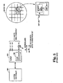
- Figure 4 illustrates a wafer probe card 400 comprising blocks 120 1 and 120 2 of the interface circuitry 116, according to another embodiment of the invention.
- the probe card 400 features a number of probes 404 for electrically connecting signal points of a DUT to its respective DUT port in the block 120 i , to allow access to such DUT.
- the probe card 400 is lowered on to the surface of a wafer to contact the signal points of the DUTs that form the wafer. Further details concerning this embodiment may be found in the patent application of Roy and Miller entitled " Interface Circuitry for Parallel Testing of Multiple Devices Under Test Using A Single Tester Channel " (P076).
- various embodiments of the invention have been described for efficient parallel testing of integrated circuit devices using a known good device to generate an expected response. For instance, by letting the tester 104 operate a KGD 112 on each channel according to a conventional test program and test sequence, the costs associated with modifying the test program to verify a number of DUTs on each channel are minimized.
- the use of the interface circuitry 116 between the DUTs and a single channel of the tester 104 permits such parallel testing of multiple DUTs per channel.
- the interface circuitry 116 is located on the wafer probe card 400, there is no need to substantially increase the number of wires between the tester 104 and the probe card 400 for testing multiple DUTs per channel, thus further promoting a high throughput yet economically efficient test system.
- certain embodiments of the invention provide the advantage that the tester, its test program and core test sequences, including margins and vectors, are not substantially affected by the invention.
- the test program is modified only slightly, such as by the addition of a short routine that reads the error information generated by the interface circuitry.
- the invention is capable of use in various other combinations and environments and is capable of changes and modifications within the scope of the inventive concept expressed here.
- the embodiments of the invention described above are particularly useful for testing memory die as part of a wafer using a wafer probe card
- the concept of parallel testing of DUTs may also be carried out at the package level where the DUTs are part of packaged IC dies.
- the error information provided by the interface circuitry may be used during a final test of packaged die to simply pass or fail an entire package rather than specify errors in exact bit locations.
Landscapes
- Engineering & Computer Science (AREA)
- General Engineering & Computer Science (AREA)
- Physics & Mathematics (AREA)
- General Physics & Mathematics (AREA)
- Tests Of Electronic Circuits (AREA)
- Testing Or Measuring Of Semiconductors Or The Like (AREA)
- Measuring Leads Or Probes (AREA)
Applications Claiming Priority (3)
| Application Number | Priority Date | Filing Date | Title |
|---|---|---|---|
| US260460 | 1999-03-01 | ||
| US09/260,460 US6452411B1 (en) | 1999-03-01 | 1999-03-01 | Efficient parallel testing of integrated circuit devices using a known good device to generate expected responses |
| PCT/US2000/004864 WO2000052487A1 (en) | 1999-03-01 | 2000-02-24 | Efficient parallel testing of integrated circuit devices using a known good device to generate expected responses |
Publications (2)
| Publication Number | Publication Date |
|---|---|
| EP1159629A1 EP1159629A1 (en) | 2001-12-05 |
| EP1159629B1 true EP1159629B1 (en) | 2008-09-10 |
Family
ID=22989261
Family Applications (1)
| Application Number | Title | Priority Date | Filing Date |
|---|---|---|---|
| EP00910351A Expired - Lifetime EP1159629B1 (en) | 1999-03-01 | 2000-02-24 | Efficient parallel testing of integrated circuit devices using a known good device to generate expected responses |
Country Status (8)
| Country | Link |
|---|---|
| US (2) | US6452411B1 (enExample) |
| EP (1) | EP1159629B1 (enExample) |
| JP (1) | JP4571749B2 (enExample) |
| KR (1) | KR100681363B1 (enExample) |
| AU (1) | AU3245800A (enExample) |
| DE (1) | DE60040212D1 (enExample) |
| TW (1) | TW451379B (enExample) |
| WO (1) | WO2000052487A1 (enExample) |
Families Citing this family (120)
| Publication number | Priority date | Publication date | Assignee | Title |
|---|---|---|---|---|
| US20020053734A1 (en) * | 1993-11-16 | 2002-05-09 | Formfactor, Inc. | Probe card assembly and kit, and methods of making same |
| US6232789B1 (en) | 1997-05-28 | 2001-05-15 | Cascade Microtech, Inc. | Probe holder for low current measurements |
| US5729150A (en) | 1995-12-01 | 1998-03-17 | Cascade Microtech, Inc. | Low-current probe card with reduced triboelectric current generating cables |
| US5914613A (en) | 1996-08-08 | 1999-06-22 | Cascade Microtech, Inc. | Membrane probing system with local contact scrub |
| US6034533A (en) | 1997-06-10 | 2000-03-07 | Tervo; Paul A. | Low-current pogo probe card |
| US6256882B1 (en) | 1998-07-14 | 2001-07-10 | Cascade Microtech, Inc. | Membrane probing system |
| US6812718B1 (en) | 1999-05-27 | 2004-11-02 | Nanonexus, Inc. | Massively parallel interface for electronic circuits |
| US7247035B2 (en) | 2000-06-20 | 2007-07-24 | Nanonexus, Inc. | Enhanced stress metal spring contactor |
| US7349223B2 (en) | 2000-05-23 | 2008-03-25 | Nanonexus, Inc. | Enhanced compliant probe card systems having improved planarity |
| US7382142B2 (en) | 2000-05-23 | 2008-06-03 | Nanonexus, Inc. | High density interconnect system having rapid fabrication cycle |
| US6578264B1 (en) | 1999-06-04 | 2003-06-17 | Cascade Microtech, Inc. | Method for constructing a membrane probe using a depression |
| US7350108B1 (en) * | 1999-09-10 | 2008-03-25 | International Business Machines Corporation | Test system for integrated circuits |
| JP4444419B2 (ja) * | 1999-11-10 | 2010-03-31 | 東京エレクトロン株式会社 | データ通信方法及びデータ通信システム |
| US6615379B1 (en) * | 1999-12-08 | 2003-09-02 | Intel Corporation | Method and apparatus for testing a logic device |
| WO2001063311A2 (en) * | 2000-02-22 | 2001-08-30 | Don Mccord | Method and system for wafer and device-level testing of an integrated circuit |
| US6838890B2 (en) | 2000-02-25 | 2005-01-04 | Cascade Microtech, Inc. | Membrane probing system |
| US7579848B2 (en) | 2000-05-23 | 2009-08-25 | Nanonexus, Inc. | High density interconnect system for IC packages and interconnect assemblies |
| US6603323B1 (en) | 2000-07-10 | 2003-08-05 | Formfactor, Inc. | Closed-grid bus architecture for wafer interconnect structure |
| US6927591B2 (en) * | 2000-09-22 | 2005-08-09 | Mccord Don | Method and system for wafer and device level testing of an integrated circuit |
| KR100358919B1 (ko) * | 2000-11-18 | 2002-10-31 | 주식회사 메모리앤테스팅 | 마스터-슬레이브방식을 이용한 반도체칩 검사장치 |
| US6629048B1 (en) * | 2000-11-20 | 2003-09-30 | Tektronix, Inc. | Measurement test instrument and associated voltage management system for accessory device |
| DE20114544U1 (de) | 2000-12-04 | 2002-02-21 | Cascade Microtech, Inc., Beaverton, Oreg. | Wafersonde |
| TW494516B (en) * | 2001-03-14 | 2002-07-11 | Winbond Electronics Corp | Semiconductor multi-die testing system with automatic identification functions |
| AU2002327490A1 (en) | 2001-08-21 | 2003-06-30 | Cascade Microtech, Inc. | Membrane probing system |
| ATE345509T1 (de) * | 2001-09-14 | 2006-12-15 | Rambus Inc | Eingebaute selbstprüfung von mehrpegelsignalschnittstellen |
| US20030070126A1 (en) * | 2001-09-14 | 2003-04-10 | Werner Carl W. | Built-in self-testing of multilevel signal interfaces |
| US7162672B2 (en) | 2001-09-14 | 2007-01-09 | Rambus Inc | Multilevel signal interface testing with binary test apparatus by emulation of multilevel signals |
| US6880118B2 (en) * | 2001-10-25 | 2005-04-12 | Sun Microsystems, Inc. | System and method for testing operational transmissions of an integrated circuit |
| US6848063B2 (en) * | 2001-11-20 | 2005-01-25 | Hewlett-Packard Development Company, L.P. | System and method for scrubbing errors in very large memories |
| US6961885B2 (en) * | 2001-11-26 | 2005-11-01 | Ati Technologies, Inc. | System and method for testing video devices using a test fixture |
| US6880116B2 (en) * | 2001-11-27 | 2005-04-12 | Ati Technologies, Inc. | System for testing multiple devices on a single system and method thereof |
| US7085980B2 (en) * | 2002-05-02 | 2006-08-01 | International Business Machines Corporation | Method and apparatus for determining the failing operation of a device-under-test |
| US6847218B1 (en) | 2002-05-13 | 2005-01-25 | Cypress Semiconductor Corporation | Probe card with an adapter layer for testing integrated circuits |
| KR100864916B1 (ko) | 2002-05-23 | 2008-10-22 | 캐스케이드 마이크로테크 인코포레이티드 | 피시험 디바이스를 테스트하기 위한 프로브 |
| US6759865B1 (en) * | 2002-07-30 | 2004-07-06 | Cypress Semiconductor Corporation | Array of dice for testing integrated circuits |
| KR100487946B1 (ko) * | 2002-08-29 | 2005-05-06 | 삼성전자주식회사 | 반도체 테스트 시스템 및 이 시스템의 테스트 방법 |
| US7119567B2 (en) * | 2002-09-12 | 2006-10-10 | Infineon Technologies North America Corp. | System and method for testing one or more dies on a semiconductor wafer |
| US6724205B1 (en) | 2002-11-13 | 2004-04-20 | Cascade Microtech, Inc. | Probe for combined signals |
| US7131046B2 (en) * | 2002-12-03 | 2006-10-31 | Verigy Ipco | System and method for testing circuitry using an externally generated signature |
| JP2004249817A (ja) * | 2003-02-19 | 2004-09-09 | Denso Corp | 電子制御装置及び複数の電子制御装置からなる制御システム |
| US7112975B1 (en) * | 2003-03-26 | 2006-09-26 | Cypress Semiconductor Corporation | Advanced probe card and method of fabricating same |
| US7057404B2 (en) | 2003-05-23 | 2006-06-06 | Sharp Laboratories Of America, Inc. | Shielded probe for testing a device under test |
| DE10338079B4 (de) * | 2003-08-19 | 2007-05-16 | Infineon Technologies Ag | Testanordnung zum Testen von Halbleiterschaltungschips |
| US7089439B1 (en) * | 2003-09-03 | 2006-08-08 | T-Ram, Inc. | Architecture and method for output clock generation on a high speed memory device |
| JP4332392B2 (ja) * | 2003-09-12 | 2009-09-16 | 株式会社アドバンテスト | 試験装置 |
| DE10345977B4 (de) * | 2003-10-02 | 2013-07-11 | Qimonda Ag | Verfahren zum Testen von zu testenden Schaltungseinheiten mittels Mehrheitsentscheidungen und Testvorrichtung zur Durchführung des Verfahrens |
| US7171586B1 (en) * | 2003-12-17 | 2007-01-30 | Sun Microsystems, Inc. | Method and apparatus for identifying mechanisms responsible for “no-trouble-found” (NTF) events in computer systems |
| JP2007517231A (ja) | 2003-12-24 | 2007-06-28 | カスケード マイクロテック インコーポレイテッド | アクティブ・ウェハプローブ |
| US7332921B2 (en) * | 2004-03-26 | 2008-02-19 | Cypress Semiconductor Corporation | Probe card and method for constructing same |
| DE102004021267B4 (de) | 2004-04-30 | 2008-04-17 | Infineon Technologies Ag | Verfahren zum Testen eines Speicherbausteins und Prüfanordnung |
| US7348887B1 (en) | 2004-06-15 | 2008-03-25 | Eigent Technologies, Llc | RFIDs embedded into semiconductors |
| KR101157449B1 (ko) | 2004-07-07 | 2012-06-22 | 캐스케이드 마이크로테크 인코포레이티드 | 멤브레인 서스펜디드 프로브를 구비한 프로브 헤드 |
| US7913002B2 (en) * | 2004-08-20 | 2011-03-22 | Advantest Corporation | Test apparatus, configuration method, and device interface |
| DE202005021435U1 (de) | 2004-09-13 | 2008-02-28 | Cascade Microtech, Inc., Beaverton | Doppelseitige Prüfaufbauten |
| US7627798B2 (en) * | 2004-10-08 | 2009-12-01 | Kabushiki Kaisha Toshiba | Systems and methods for circuit testing using LBIST |
| US7330038B2 (en) * | 2004-12-14 | 2008-02-12 | Silicon Light Machines Corporation | Interleaved MEMS-based probes for testing integrated circuits |
| KR100688517B1 (ko) * | 2005-01-11 | 2007-03-02 | 삼성전자주식회사 | 전압공급유닛 분할을 통한 반도체 소자의 병렬검사 방법 |
| US7656172B2 (en) | 2005-01-31 | 2010-02-02 | Cascade Microtech, Inc. | System for testing semiconductors |
| US7535247B2 (en) | 2005-01-31 | 2009-05-19 | Cascade Microtech, Inc. | Interface for testing semiconductors |
| US7712674B1 (en) | 2005-02-22 | 2010-05-11 | Eigent Technologies Llc | RFID devices for verification of correctness, reliability, functionality and security |
| US7449899B2 (en) | 2005-06-08 | 2008-11-11 | Cascade Microtech, Inc. | Probe for high frequency signals |
| JP5080459B2 (ja) | 2005-06-13 | 2012-11-21 | カスケード マイクロテック インコーポレイテッド | 広帯域能動/受動差動信号プローブ |
| DE102005037236A1 (de) * | 2005-08-08 | 2007-02-15 | Robert Bosch Gmbh | Vorrichtung und Verfahren zur Konfiguration einer Halbleiterschaltung |
| US7539912B2 (en) | 2005-12-15 | 2009-05-26 | King Tiger Technology, Inc. | Method and apparatus for testing a fully buffered memory module |
| US7532492B2 (en) * | 2005-12-20 | 2009-05-12 | Tektronix, Inc. | Host controlled voltage input system for an accessory device |
| JP4571076B2 (ja) * | 2006-01-23 | 2010-10-27 | 富士通セミコンダクター株式会社 | 半導体装置の検査装置 |
| US7906982B1 (en) | 2006-02-28 | 2011-03-15 | Cypress Semiconductor Corporation | Interface apparatus and methods of testing integrated circuits using the same |
| CN101030160B (zh) * | 2006-03-02 | 2013-03-20 | 鸿富锦精密工业(深圳)有限公司 | 统一串行接口测试命令的测试装置及其测试方法 |
| US7669090B2 (en) * | 2006-05-18 | 2010-02-23 | Kabushiki Kaisha Toshiba | Apparatus and method for verifying custom IC |
| DE202007018733U1 (de) | 2006-06-09 | 2009-03-26 | Cascade Microtech, Inc., Beaverton | Messfühler für differentielle Signale mit integrierter Symmetrieschaltung |
| US7723999B2 (en) | 2006-06-12 | 2010-05-25 | Cascade Microtech, Inc. | Calibration structures for differential signal probing |
| US7764072B2 (en) | 2006-06-12 | 2010-07-27 | Cascade Microtech, Inc. | Differential signal probing system |
| US7443186B2 (en) | 2006-06-12 | 2008-10-28 | Cascade Microtech, Inc. | On-wafer test structures for differential signals |
| US7403028B2 (en) | 2006-06-12 | 2008-07-22 | Cascade Microtech, Inc. | Test structure and probe for differential signals |
| KR20090036144A (ko) * | 2006-08-14 | 2009-04-13 | 가부시키가이샤 어드밴티스트 | 시험 장치 및 시험 방법 |
| US7649366B2 (en) | 2006-09-01 | 2010-01-19 | Formfactor, Inc. | Method and apparatus for switching tester resources |
| US7890822B2 (en) * | 2006-09-29 | 2011-02-15 | Teradyne, Inc. | Tester input/output sharing |
| JP5151988B2 (ja) | 2006-11-10 | 2013-02-27 | 日本電気株式会社 | テスト回路と方法並びに半導体装置 |
| WO2008056609A1 (fr) * | 2006-11-10 | 2008-05-15 | Nec Corporation | Circuit de test en parallèle et procédé et dispositif semi-conducteur |
| US20080133165A1 (en) * | 2006-12-04 | 2008-06-05 | Advantest Corporation | Test apparatus and device interface |
| US7852094B2 (en) * | 2006-12-06 | 2010-12-14 | Formfactor, Inc. | Sharing resources in a system for testing semiconductor devices |
| US7669100B2 (en) * | 2007-03-08 | 2010-02-23 | Freescale Semiconductor, Inc. | System and method for testing and providing an integrated circuit having multiple modules or submodules |
| US7610538B2 (en) * | 2007-04-13 | 2009-10-27 | Advantest Corporation | Test apparatus and performance board for diagnosis |
| US7620861B2 (en) * | 2007-05-31 | 2009-11-17 | Kingtiger Technology (Canada) Inc. | Method and apparatus for testing integrated circuits by employing test vector patterns that satisfy passband requirements imposed by communication channels |
| US7876114B2 (en) | 2007-08-08 | 2011-01-25 | Cascade Microtech, Inc. | Differential waveguide probe |
| US7757144B2 (en) * | 2007-11-01 | 2010-07-13 | Kingtiger Technology (Canada) Inc. | System and method for testing integrated circuit modules comprising a plurality of integrated circuit devices |
| US20090119542A1 (en) * | 2007-11-05 | 2009-05-07 | Advantest Corporation | System, method, and program product for simulating test equipment |
| US8022718B2 (en) * | 2008-02-29 | 2011-09-20 | Lam Research Corporation | Method for inspecting electrostatic chucks with Kelvin probe analysis |
| JPWO2009147724A1 (ja) * | 2008-06-02 | 2011-10-20 | 株式会社アドバンテスト | 試験用ウエハユニットおよび試験システム |
| US7848899B2 (en) * | 2008-06-09 | 2010-12-07 | Kingtiger Technology (Canada) Inc. | Systems and methods for testing integrated circuit devices |
| US7888957B2 (en) | 2008-10-06 | 2011-02-15 | Cascade Microtech, Inc. | Probing apparatus with impedance optimized interface |
| US7948254B2 (en) | 2008-11-20 | 2011-05-24 | Litepoint Corporation | Digital communications test system for multiple input, multiple output (MIMO) systems |
| US8410806B2 (en) | 2008-11-21 | 2013-04-02 | Cascade Microtech, Inc. | Replaceable coupon for a probing apparatus |
| JP5414292B2 (ja) * | 2009-01-29 | 2014-02-12 | ルネサスエレクトロニクス株式会社 | 不良解析装置と方法及びプログラム |
| US8356215B2 (en) * | 2010-01-19 | 2013-01-15 | Kingtiger Technology (Canada) Inc. | Testing apparatus and method for analyzing a memory module operating within an application system |
| CN103003708B (zh) * | 2010-04-14 | 2015-01-07 | 爱德万测试(新加坡)私人有限公司 | 用于测试多个被测器件的装置和方法 |
| US8918686B2 (en) | 2010-08-18 | 2014-12-23 | Kingtiger Technology (Canada) Inc. | Determining data valid windows in a system and method for testing an integrated circuit device |
| US8560903B2 (en) | 2010-08-31 | 2013-10-15 | Cisco Technology, Inc. | System and method for executing functional scanning in an integrated circuit environment |
| CN102466775B (zh) * | 2010-11-17 | 2014-11-05 | 益明精密科技有限公司 | 多功能可变换模块测试装置 |
| US8560474B2 (en) | 2011-03-07 | 2013-10-15 | Cisco Technology, Inc. | System and method for providing adaptive manufacturing diagnoses in a circuit board environment |
| US9003256B2 (en) | 2011-09-06 | 2015-04-07 | Kingtiger Technology (Canada) Inc. | System and method for testing integrated circuits by determining the solid timing window |
| US10776233B2 (en) | 2011-10-28 | 2020-09-15 | Teradyne, Inc. | Programmable test instrument |
| US9759772B2 (en) | 2011-10-28 | 2017-09-12 | Teradyne, Inc. | Programmable test instrument |
| US8724408B2 (en) | 2011-11-29 | 2014-05-13 | Kingtiger Technology (Canada) Inc. | Systems and methods for testing and assembling memory modules |
| US9117552B2 (en) | 2012-08-28 | 2015-08-25 | Kingtiger Technology(Canada), Inc. | Systems and methods for testing memory |
| US9470753B2 (en) * | 2012-11-07 | 2016-10-18 | Cascade Microtech, Inc. | Systems and methods for testing electronic devices that include low power output drivers |
| US9678148B2 (en) * | 2014-06-06 | 2017-06-13 | Advantest Corporation | Customizable tester having testing modules for automated testing of devices |
| US9933454B2 (en) | 2014-06-06 | 2018-04-03 | Advantest Corporation | Universal test floor system |
| US9638749B2 (en) | 2014-06-06 | 2017-05-02 | Advantest Corporation | Supporting automated testing of devices in a test floor system |
| US9618574B2 (en) | 2014-06-06 | 2017-04-11 | Advantest Corporation | Controlling automated testing of devices |
| US9618570B2 (en) * | 2014-06-06 | 2017-04-11 | Advantest Corporation | Multi-configurable testing module for automated testing of a device |
| WO2016173619A1 (en) | 2015-04-27 | 2016-11-03 | Advantest Corporation | Switch circuit, method for operating a switch circuit and an automated test equipment |
| KR20160138766A (ko) * | 2015-05-26 | 2016-12-06 | 에스케이하이닉스 주식회사 | 반도체 장치 |
| WO2016188572A1 (en) | 2015-05-27 | 2016-12-01 | Advantest Corporation | Automated test equipment for combined signals |
| US9858177B2 (en) | 2015-10-30 | 2018-01-02 | International Business Machines Corporation | Automated test generation for multi-interface enterprise virtualization management environment |
| US10572373B2 (en) | 2017-04-20 | 2020-02-25 | International Business Machines Corporation | Automated test generation for multi-interface and multi-platform enterprise virtualization management environment |
| KR102471500B1 (ko) * | 2018-03-12 | 2022-11-28 | 에스케이하이닉스 주식회사 | 반도체 장치 및 이를 포함하는 테스트 시스템 |
| US10794955B2 (en) * | 2018-10-16 | 2020-10-06 | Optimal Plus Ltd | Methods and systems for testing a tester |
| JP7058759B2 (ja) * | 2019-01-22 | 2022-04-22 | 株式会社アドバンテスト | 1または複数の被テストデバイスをテストするための自動試験装置、1または複数の被テストデバイスの自動試験のための方法、および、コマンドエラーを処理するためのコンピュータプログラム |
| CN116948923B (zh) * | 2023-09-21 | 2023-12-08 | 内蒙古农业大学 | 一种可实现生物结皮-植物立体防护模式的生物引发剂 |
Family Cites Families (34)
| Publication number | Priority date | Publication date | Assignee | Title |
|---|---|---|---|---|
| IT1003048B (it) * | 1972-03-17 | 1976-06-10 | Honeywell Inf Systems | Dispositivo per verificare il cor retto comportamento di unita circui tali integrate sequenziali |
| US4370746A (en) | 1980-12-24 | 1983-01-25 | International Business Machines Corporation | Memory address selector |
| US4455654B1 (en) | 1981-06-05 | 1991-04-30 | Test apparatus for electronic assemblies employing a microprocessor | |
| US4773028A (en) * | 1984-10-01 | 1988-09-20 | Tektronix, Inc. | Method and apparatus for improved monitoring and detection of improper device operation |
| JPS6199876A (ja) | 1984-10-22 | 1986-05-17 | Nec Corp | Icテスタ− |
| US4942576A (en) | 1988-10-24 | 1990-07-17 | Micron Technology, Inc. | Badbit counter for memory testing |
| US5070297A (en) | 1990-06-04 | 1991-12-03 | Texas Instruments Incorporated | Full wafer integrated circuit testing device |
| FI91356C (fi) | 1990-07-11 | 1994-06-27 | Instrumentarium Oy | Verenpainemittauksessa käytettävän mansetin paineen rajoittaminen |
| JP2773483B2 (ja) * | 1991-09-24 | 1998-07-09 | 三菱電機株式会社 | 半導体試験装置 |
| US5357523A (en) | 1991-12-18 | 1994-10-18 | International Business Machines Corporation | Memory testing system with algorithmic test data generation |
| US5648661A (en) | 1992-07-02 | 1997-07-15 | Lsi Logic Corporation | Integrated circuit wafer comprising unsingulated dies, and decoder arrangement for individually testing the dies |
| US5442282A (en) | 1992-07-02 | 1995-08-15 | Lsi Logic Corporation | Testing and exercising individual, unsingulated dies on a wafer |
| JPH0627195A (ja) | 1992-07-08 | 1994-02-04 | Mitsubishi Electric Corp | Lsi試験装置 |
| US5243274A (en) | 1992-08-07 | 1993-09-07 | Westinghouse Electric Corp. | Asic tester |
| US5477160A (en) | 1992-08-12 | 1995-12-19 | Fujitsu Limited | Module test card |
| US5363038A (en) | 1992-08-12 | 1994-11-08 | Fujitsu Limited | Method and apparatus for testing an unpopulated chip carrier using a module test card |
| KR970010656B1 (ko) | 1992-09-01 | 1997-06-30 | 마쯔시다 덴기 산교 가부시끼가이샤 | 반도체 테스트 장치, 반도체 테스트 회로칩 및 프로브 카드 |
| US6064213A (en) | 1993-11-16 | 2000-05-16 | Formfactor, Inc. | Wafer-level burn-in and test |
| US6577148B1 (en) | 1994-08-31 | 2003-06-10 | Motorola, Inc. | Apparatus, method, and wafer used for testing integrated circuits formed on a product wafer |
| US5682472A (en) | 1995-03-17 | 1997-10-28 | Aehr Test Systems | Method and system for testing memory programming devices |
| US5506499A (en) | 1995-06-05 | 1996-04-09 | Neomagic Corp. | Multiple probing of an auxilary test pad which allows for reliable bonding to a primary bonding pad |
| JP2737774B2 (ja) * | 1996-03-15 | 1998-04-08 | 日本電気株式会社 | ウェハテスタ |
| US5839100A (en) | 1996-04-22 | 1998-11-17 | Wegener; Albert William | Lossless and loss-limited compression of sampled data signals |
| US5689515A (en) | 1996-04-26 | 1997-11-18 | Teradyne, Inc. | High speed serial data pin for automatic test equipment |
| US5995915A (en) | 1997-01-29 | 1999-11-30 | Advanced Micro Devices, Inc. | Method and apparatus for the functional verification of digital electronic systems |
| US5923178A (en) | 1997-04-17 | 1999-07-13 | Cerprobe Corporation | Probe assembly and method for switchable multi-DUT testing of integrated circuit wafers |
| US5910895A (en) | 1997-06-13 | 1999-06-08 | Teradyne, Inc. | Low cost, easy to use automatic test system software |
| US5995424A (en) | 1997-07-16 | 1999-11-30 | Tanisys Technology, Inc. | Synchronous memory test system |
| US5794175A (en) | 1997-09-09 | 1998-08-11 | Teradyne, Inc. | Low cost, highly parallel memory tester |
| US6064948A (en) | 1998-03-02 | 2000-05-16 | Tanisys Technology, Inc. | Tester systems |
| US6246250B1 (en) | 1998-05-11 | 2001-06-12 | Micron Technology, Inc. | Probe card having on-board multiplex circuitry for expanding tester resources |
| US6275962B1 (en) | 1998-10-23 | 2001-08-14 | Teradyne, Inc. | Remote test module for automatic test equipment |
| US6324665B1 (en) * | 1998-11-03 | 2001-11-27 | Agilent Technologies, Inc. | Event based fault diagnosis |
| US6256760B1 (en) | 1998-11-13 | 2001-07-03 | Nortel Networks Limited | Automatic test equipment scan test enhancement |
-
1999
- 1999-03-01 US US09/260,460 patent/US6452411B1/en not_active Expired - Fee Related
-
2000
- 2000-02-24 KR KR1020017011121A patent/KR100681363B1/ko not_active Expired - Fee Related
- 2000-02-24 AU AU32458/00A patent/AU3245800A/en not_active Abandoned
- 2000-02-24 DE DE60040212T patent/DE60040212D1/de not_active Expired - Lifetime
- 2000-02-24 JP JP2000602648A patent/JP4571749B2/ja not_active Expired - Fee Related
- 2000-02-24 EP EP00910351A patent/EP1159629B1/en not_active Expired - Lifetime
- 2000-02-24 WO PCT/US2000/004864 patent/WO2000052487A1/en not_active Ceased
- 2000-02-25 TW TW089103419A patent/TW451379B/zh not_active IP Right Cessation
-
2002
- 2002-07-29 US US10/208,173 patent/US6559671B2/en not_active Expired - Fee Related
Also Published As
| Publication number | Publication date |
|---|---|
| KR100681363B1 (ko) | 2007-02-12 |
| US6559671B2 (en) | 2003-05-06 |
| EP1159629A1 (en) | 2001-12-05 |
| WO2000052487A1 (en) | 2000-09-08 |
| AU3245800A (en) | 2000-09-21 |
| TW451379B (en) | 2001-08-21 |
| KR20010104363A (ko) | 2001-11-24 |
| JP4571749B2 (ja) | 2010-10-27 |
| JP2002538464A (ja) | 2002-11-12 |
| US6452411B1 (en) | 2002-09-17 |
| US20020175697A1 (en) | 2002-11-28 |
| DE60040212D1 (de) | 2008-10-23 |
Similar Documents
| Publication | Publication Date | Title |
|---|---|---|
| EP1159629B1 (en) | Efficient parallel testing of integrated circuit devices using a known good device to generate expected responses | |
| EP1159630B1 (en) | Distributed interface for parallel testing of multiple devices using a single tester channel | |
| US6480978B1 (en) | Parallel testing of integrated circuit devices using cross-DUT and within-DUT comparisons | |
| US7826996B2 (en) | Memory-daughter-card-testing apparatus and method | |
| US6668347B1 (en) | Built-in self-testing for embedded memory | |
| US6256760B1 (en) | Automatic test equipment scan test enhancement | |
| CN100399473C (zh) | 内置自测系统和方法 | |
| US7844867B1 (en) | Combined processor access and built in self test in hierarchical memory systems | |
| WO2001073459A2 (en) | System and method for testing signal interconnections using built-in self test | |
| US7353442B2 (en) | On-chip and at-speed tester for testing and characterization of different types of memories | |
| WO2002025957A2 (en) | Memory module and memory component built-in self test | |
| WO2007114373A1 (ja) | テスト方法、テストシステムおよび補助基板 | |
| EP1411434A2 (en) | A software programmable verification tool having a single built-in self-test (bist) module for testing and debugging multiple memory modules in a device under test (dut) | |
| US6374376B1 (en) | Circuit, system and method for arranging data output by semiconductor testers to packet-based devices under test | |
| US5978945A (en) | Tester arrangement comprising a connection module for testing, by way of the boundary scan test method, a carrier provided with a first number of digital ICS with BST logic and a second number of digital ICS without BST logic | |
| KR100786414B1 (ko) | Dut 테스터 데이터 채널 반전 특성 관리 장치 |
Legal Events
| Date | Code | Title | Description |
|---|---|---|---|
| PUAI | Public reference made under article 153(3) epc to a published international application that has entered the european phase |
Free format text: ORIGINAL CODE: 0009012 |
|
| 17P | Request for examination filed |
Effective date: 20010928 |
|
| AK | Designated contracting states |
Kind code of ref document: A1 Designated state(s): AT BE CH CY DE DK ES FI FR GB GR IE IT LI LU MC NL PT SE |
|
| RAP1 | Party data changed (applicant data changed or rights of an application transferred) |
Owner name: FORMFACTOR, INC. |
|
| 17Q | First examination report despatched |
Effective date: 20021210 |
|
| RBV | Designated contracting states (corrected) |
Designated state(s): DE FR GB IT |
|
| RAP1 | Party data changed (applicant data changed or rights of an application transferred) |
Owner name: FORMFACTOR, INC. |
|
| GRAP | Despatch of communication of intention to grant a patent |
Free format text: ORIGINAL CODE: EPIDOSNIGR1 |
|
| GRAS | Grant fee paid |
Free format text: ORIGINAL CODE: EPIDOSNIGR3 |
|
| GRAA | (expected) grant |
Free format text: ORIGINAL CODE: 0009210 |
|
| AK | Designated contracting states |
Kind code of ref document: B1 Designated state(s): DE FR GB IT |
|
| REG | Reference to a national code |
Ref country code: GB Ref legal event code: FG4D |
|
| REF | Corresponds to: |
Ref document number: 60040212 Country of ref document: DE Date of ref document: 20081023 Kind code of ref document: P |
|
| PLBE | No opposition filed within time limit |
Free format text: ORIGINAL CODE: 0009261 |
|
| STAA | Information on the status of an ep patent application or granted ep patent |
Free format text: STATUS: NO OPPOSITION FILED WITHIN TIME LIMIT |
|
| 26N | No opposition filed |
Effective date: 20090611 |
|
| GBPC | Gb: european patent ceased through non-payment of renewal fee |
Effective date: 20090224 |
|
| REG | Reference to a national code |
Ref country code: FR Ref legal event code: ST Effective date: 20091030 |
|
| PG25 | Lapsed in a contracting state [announced via postgrant information from national office to epo] |
Ref country code: GB Free format text: LAPSE BECAUSE OF NON-PAYMENT OF DUE FEES Effective date: 20090224 Ref country code: FR Free format text: LAPSE BECAUSE OF NON-PAYMENT OF DUE FEES Effective date: 20090302 |
|
| PGFP | Annual fee paid to national office [announced via postgrant information from national office to epo] |
Ref country code: IT Payment date: 20100224 Year of fee payment: 11 |
|
| PGFP | Annual fee paid to national office [announced via postgrant information from national office to epo] |
Ref country code: DE Payment date: 20100226 Year of fee payment: 11 |
|
| PG25 | Lapsed in a contracting state [announced via postgrant information from national office to epo] |
Ref country code: IT Free format text: LAPSE BECAUSE OF NON-PAYMENT OF DUE FEES Effective date: 20110224 |
|
| REG | Reference to a national code |
Ref country code: DE Ref legal event code: R119 Ref document number: 60040212 Country of ref document: DE Effective date: 20110901 |
|
| PG25 | Lapsed in a contracting state [announced via postgrant information from national office to epo] |
Ref country code: DE Free format text: LAPSE BECAUSE OF NON-PAYMENT OF DUE FEES Effective date: 20110901 |