EP1156603A2 - Circuit de commande d'une diode electroluminescente et module d'émission optique - Google Patents
Circuit de commande d'une diode electroluminescente et module d'émission optique Download PDFInfo
- Publication number
- EP1156603A2 EP1156603A2 EP01111278A EP01111278A EP1156603A2 EP 1156603 A2 EP1156603 A2 EP 1156603A2 EP 01111278 A EP01111278 A EP 01111278A EP 01111278 A EP01111278 A EP 01111278A EP 1156603 A2 EP1156603 A2 EP 1156603A2
- Authority
- EP
- European Patent Office
- Prior art keywords
- led
- voltage
- pulse
- output
- circuit
- Prior art date
- Legal status (The legal status is an assumption and is not a legal conclusion. Google has not performed a legal analysis and makes no representation as to the accuracy of the status listed.)
- Withdrawn
Links
Images


Classifications
-
- G—PHYSICS
- G09—EDUCATION; CRYPTOGRAPHY; DISPLAY; ADVERTISING; SEALS
- G09G—ARRANGEMENTS OR CIRCUITS FOR CONTROL OF INDICATING DEVICES USING STATIC MEANS TO PRESENT VARIABLE INFORMATION
- G09G3/00—Control arrangements or circuits, of interest only in connection with visual indicators other than cathode-ray tubes
- G09G3/20—Control arrangements or circuits, of interest only in connection with visual indicators other than cathode-ray tubes for presentation of an assembly of a number of characters, e.g. a page, by composing the assembly by combination of individual elements arranged in a matrix no fixed position being assigned to or needed to be assigned to the individual characters or partial characters
-
- H—ELECTRICITY
- H04—ELECTRIC COMMUNICATION TECHNIQUE
- H04B—TRANSMISSION
- H04B10/00—Transmission systems employing electromagnetic waves other than radio-waves, e.g. infrared, visible or ultraviolet light, or employing corpuscular radiation, e.g. quantum communication
- H04B10/50—Transmitters
- H04B10/501—Structural aspects
- H04B10/502—LED transmitters
-
- H—ELECTRICITY
- H04—ELECTRIC COMMUNICATION TECHNIQUE
- H04B—TRANSMISSION
- H04B10/00—Transmission systems employing electromagnetic waves other than radio-waves, e.g. infrared, visible or ultraviolet light, or employing corpuscular radiation, e.g. quantum communication
- H04B10/50—Transmitters
- H04B10/508—Pulse generation, e.g. generation of solitons
Definitions
- the present invention relates to an LED intensity modulation type driving circuit for controlling emission/non-emission of an LED output in accordance with the high/low level of an input voltage pulse and, more particularly, to an LED driving circuit capable of outputting a high-speed modulated optical signal almost free from an emission pulse waveform distortion that is inevitable in optical data transmission of a high-speed optical data link.
- Multimedia data now widely-used and being increasingly developed, is typically exchanged over a variety of high-speed optical network backbones throughout the world.
- optical transmitting and receiving modules play an important role as key components in optical communication systems of long-distance LAN connections, and short to mid-distance LANs supported by fiber-optic channels and Gigabit Ethernet.
- Purpose-built optical transmitting and receiving modules used in IT (Information Technology) systems currently in use have been developed at a cost, sacrificing versatility at the same time.
- IEEE 1394a extended from the electrical specification IEEE 1394 standardized in 1995 is further extended to optical applications, promoting standardization of IEEE 1394b which targets an optical data link using a POF (Plastic Optical Fiber) and is applicable to high-speed, low-cost, medium-distance connection.
- POF Physical Optical Fiber
- practical performance is important as an interconnect requirements specification in addition to specifications which define basic transmission performance such as high throughput, regardless of the optical or electrical transmission signal form.
- the standard draft IEEE 1394b under examination adopts a gradient index plastic optical fiber having a large core system in order to reduce the cost of an optical fiber for use, simplify the internal structure, and reduce the cost of an optical link module itself.
- An example of this plastic optical fiber is combined with a red light source which falls within the low-loss wavelength region of the fiber.
- the light source of the red wavelength region is a light-emitting diode (LED) which emits light in a wavelength region around 650 nm, or an optical semiconductor laser (LD) which oscillates at 650 nm.
- LED light-emitting diode
- LD optical semiconductor laser
- the LD must be employed in terms of essential element response characteristics in high-speed S800 or more which is considered to be the mainstream of the optical data link as the technique to be established in the near future.
- low-speed standards S100 to S400 will mainly adopt LEDs which can simplify the circuit arrangement and optical coupling system of an optical transmitter that are important factors for reducing the module cost.
- FIG. 2 is a basic block diagram showing a conventional optical transmitting circuit.
- a constant current pulse prepared by ON/OFF-modulating, using a transistor switch, a DC current generated by a constant current source is generated, and the output is applied to a load LED.
- This method does not pose any technical problems in a low-speed link, up to about 10 Mb/s.
- the switch response characteristic of an optical signal is low due to a large internal capacitance of a device that is a property unique to the LED. The low response characteristic determines the optical data link speed.
- a peaking pulse current in phase with a constant current pulse is superimposed on an ON/OFF-modulated driving constant current pulse in synchronism with level inversion of the driving current switch, thereby accelerating the transient response of the LED.
- the original transmission data rate is as low as several tens of Mb/s, and the essential time constant which determines the device speed unique to the LED is as short as several ns or less.
- the signal processing speeds of photoelectric conversion and logic level conversion after optical transmission are substantially negligible with the development of the IC process technique.
- Optical transmission can be realized in which the signal error rate in data transmission is suppressed to be low so as not to cause any practical problems.
- one of the present inventors has proposed a method capable of transmitting data at around 100 Mb/s by adopting the principle of current peaking driving, devising peaking superimposition, and decreasing the LED driving amplitude.
- a current bias required for an LED to generate an ON light intensity is always supplied from a DC constant current source to the LED anode.
- a CMOS buffer converts an external pulse signal input Vp into a rectangular pulse which changes at a low impedance between power supply voltages Vdd and Vss.
- a bias current input to the LED anode is ON/OFF-modulated by using the pulse.
- a differential current flowing through a capacitance Cp is superimposed and supplied as a peaking current to the LED anode.
- a method using an inductor instead of current peaking using a capacitance has also been proposed.
- the circuit shown in FIG. 1 that is driven by a conventional constant current switch is used as a main arrangement.
- a circuit constituted by series-connecting an inductor and resistor is parallel-connected to an LED, and they are driven as the entire load of the current output in place of using only the LED as a load. That is, a peaking current is generated by the inductor in transition and supplied to the LED.
- Adding the means for superimposing the peaking current can shorten the transient response time of an output optical signal to some extent.
- effective peaking superimposition inhibits a peaking pulse from completing attenuation within the signal pulse width because of the time constant. A pulse tail or the like is generated, and the bit rate cannot be so increased. Further, the output optical pulse width essentially becomes smaller than the driving pulse width of an electrical signal.
- the optical pulse width decreases by 1 ns or more in general, and in some cases by 10 ns, which depends on the LED driving circuit method. These values cannot be ignored when the minimum pulse width of a transmission optical signal is 10 ns or less. The decrease causes great variations in the ON/OFF pulse duty ratio of the transmission signal or additional increase in time jitter, seriously influencing the transmission waveform quality.
- the phenomenon that an output optical pulse becomes narrower than a driving pulse input to an LED results from a property unique to a device in which an LED generates light almost proportionally to a forward current flowing through the diode.
- the electrical equivalent circuit model of the diode is expressed by a structure as shown in FIG. 24 in which a current flows through a series resistance Rs of the diode and a p-n junction diode capacitance Cd is parallel-connected to a constant current source Id.
- Id an output current If from the constant current source Id depends on an intrinsic diode voltage vd applied across Id or Cd.
- Is be the saturation current of diode junction
- N be the radiation coefficient
- Vt kT/q (k: Boltzmann constant
- q electron charge) be the thermal electromotive force with respect to an operation temperature T of the p-n junction
- If Is ⁇ exp[Vd/(N ⁇ Vt)].
- Cd increases depending on the voltage Vd, and substantially exhibits a value dominated by the p-n junction capacitance Cj.
- the transition time capacitance component which increases in proportion to the forward current If is added.
- a general LED has Rs of several ⁇ to several tens of ⁇ and has a value of several ten pF to several hundred pF only by Cj in zero bias.
- Vh an ideal rectangular pulse
- the internal intrinsic diode voltage Vd changes by an exponential attenuation function with a time constant (Rs ⁇ Cd) of a little less than 1 ns to about 10 ns, and exhibits a waveform which is asymptotic to a steady-state value Vhigh upon the lapse of time.
- the forward current If exponentially increases with respect to Vd, as represented by the above equation.
- the forward current If reaches the same current value as the steady-state value only when the forward current If falls within (N ⁇ Vt) with respect to the value Vd at which a desired maximum steady-state current is obtained, e.g., comes near to, e.g., 30 mV to 50 mV.
- a peaking current is superimposed, like the prior art, in order to decrease the signal delay of the transient response, the charge/discharge time with respect to Cd can be shortened to shorten the delay time.
- a current exceeding the steady-state peak value of If necessary for obtaining an optical signal amplitude is supplied.
- Current consumption in operation increases, and the optical output waveform itself has peaking and deforms from the rectangle. Consequently, the discrimination level of the high-speed receiving circuit varies, and the time jitter of a reception output signal increases.
- an LD used in high-speed optical communication can obtain laser oscillation by limiting the space area to a narrow one within the element and realizing a region having a large optical amplification gain.
- the total area occupied by the element itself to be substantially operated suffices to be small.
- the unique capacitance value of the element is 10 pF or less at most.
- a large optical output can be obtained with high photoconversion efficiency in proportion to the difference from the threshold of an injection current to the element at the boundary of a current having a given threshold or more. It is, therefore, effective to turn on/off a constant current source as a reference at a high speed and convert a current into a current pulse. This method has been applied to most LD driving circuits.
- the LD can employ a normal high-frequency circuit technique in which even when the output terminal of a current switch circuit and the LD are apart from each other, they are connected via a transmission line of 50 ⁇ to match all impedances.
- the LED can always obtain an optical output proportional to an input current regardless of the magnitude of the injection current, but is essentially difficult to realize high-frequency modulation using an electrical signal because a large capacitance is added.
- An LED driving circuit comprises a voltage generation circuit for generating a first output voltage of a low level and a second output voltage of a high level, a first MOS switch for transferring the first output voltage to an output terminal, a second MOS switch for transferring the second output voltage to the output terminal, and a pulse generation circuit for shaping a waveform of an externally input signal and generating first and second rectangular pulses having a complementary relationship, wherein an LED is electrically connected to the output terminal, the first rectangular pulse is input to a gate of the first MOS switch, the second rectangular pulse is input to a gate of the second MOS switch, the high level is determined by a forward peak current or forward voltage of the LED which is necessary for outputting light of a predetermined intensity from the LED, and the low level is set to a voltage value for changing an emission intensity of the LED to zero or a negligible value.
- An LED driving circuit comprises a voltage generation circuit for generating a first output voltage of low level, a second output voltage of a first high level, and a third output voltage of a second high level which is higher than the first high level, a first MOS switch for transferring the first output voltage to an output terminal, a second MOS switch for transferring the second output voltage to the output terminal, a third MOS switch for transferring the third output voltage to the output terminal, and a pulse generation circuit for shaping a waveform of an externally input signal and generating first, second, and third rectangular pulses, wherein an LED is electrically connected to the output terminal, the first rectangular pulse is input to a gate of the first MOS switch, the second rectangular pulse is input to a gate of the second MOS switch, the third rectangular pulse is input to a gate of the third MOS switch, after the third rectangular pulse changes to the high level, the second rectangular pulse successively changes to the high level, the first rectangular pulse has a complementary relationship with an OR value of the second and third rectangular pulses, and
- An optical transmitting module comprises an IC having the above-described LED driving circuit, an LED connected to an output terminal of the LED driving circuit, a submodule on which the IC and the LED are mounted, an optical connector which is optically coupled to the LED, a lead which is electrically coupled to the IC and the LED, and a package for housing the IC, the LED, the submodule, the optical connector, and the lead.
- the phenomenon that an output optical pulse becomes narrower than a driving pulse input to an LED is caused by a property unique to a device in which an LED electrically operates as a diode and outputs a light intensity almost proportional to a forward current flowing through the diode.
- FIG. 24 An equivalent circuit model representing the electrical characteristics of the LED is shown in FIG. 24.
- the technical key point of an LED driving circuit for obtaining a high-speed optical signal is to modulate a voltage waveform around the peak value Vhigh of Vd at a high speed.
- the voltage which dominates the emission characteristics of the LED is around the peak value of Vd.
- the Cd value is fixed to the peak value of Vd.
- the result derived based on this approximation is almost the same as a numerical analysis simulation result based on an actual device mode, so the gist of the contents of the present invention described below will not change.
- a capacitive load of about 100 pF can be effectively driven by a high-speed rectangular pulse waveform by using a voltage pulse generation source having an output impedance smaller than the impedance of the load that is smaller in the high-frequency region.
- ideal rectangular pulse driving can be realized by directly applying a rectangular voltage pulse to the LED.
- an externally input pulse is shaped into a rectangular pulse, and a rectangular voltage pulse which changes to a high level the voltage Vhigh having a value corresponding to Vd at which If necessary for causing the LED to emit light at a desired luminance is obtained is generated, output, and applied to the external load LED.
- its output impedance is desirably set to 1/5 or less the Rs value.
- the low level value Vlow of the output voltage pulse is set to 0V or more equal to ground to which the cathode of the LED is connected, and to a voltage corresponding to a forward current of 1 ⁇ A or less at which emission of the LED can be ignored in the entire operation temperature range, e.g., to 1.4V or less for a 650-nm LED.
- the rise waveform of Vd is limited by the RC time constant of the series resistance Rs and total diode capacitance Cd of the LED even by driving with the rectangular voltage pulse.
- the limited amount depends on an LED element for use, and the value of the time constant Rs ⁇ Cd varies from 1 ns to 20 ns.
- the maximum value of a bit rate allowing transmission is determined not by the transient response time of the driving circuit itself but by the time constant of the element.
- the rise of an emission pulse greatly delays from an input rectangular voltage pulse at the pulse rise portion, whereas no large delay occurs at the fall of the input voltage pulse in comparison with the rise because a current flowing through the LED abruptly decreases when the application voltage of the intrinsic diode drops and reaches several tens of mA with respect to the peak value Vhigh.
- the rise delay cannot be ignored, but the fall delay can be substantially ignored.
- the pulse width narrowing phenomenon occurs even when high-speed operation is enabled by adopting a driving method with a rectangular voltage pulse.
- the low level value Vl of the pulse voltage applied to the LED is controlled. That is, when the flow of electric charges which raise the capacitive load is limited, the charge time is shortened by decreasing the voltage difference to be changed from the beginning.
- the voltage is set to be lower than a forward voltage which gives a current value obtained by dividing If which gives high-level output light by an extinction ratio required for an LED output optical signal, and to be as high as possible within a voltage range where the low level value of a repetitive optical output pulse signal at the maximum frequency can ensure a value twice or less the low level value of a low-speed repetitive optical pulse signal. Resultantly, the voltage pulse amplitude for driving the LED is minimized, the charge amount necessary for charging/discharging Cd is minimized, the driving current is suppressed, and power consumption is secondarily reduced.
- a current injected to Cd is increased. Since the impedance which limits charge injection is fixed to Rs, the voltage applied across Rs, i.e., voltage applied to the LED is set higher than Vh in the initial time of pulse transition.
- the pulse waveform output to the LED deforms from a rectangular shape which keeps an ideal constant high level, and the LED is driven by a voltage pulse of a waveform having two high level values.
- a high-level application voltage is set to a voltage Vh2 higher than Vh during a predetermined period after the start of the pulse leading edge until the voltage Vd reaches Vh.
- Vd reaches an intended steady-state value Vh
- the high-level voltage value Vh1 returns to the prescribed value Vh and keeps constant at Vh during the remaining high-pulse period.
- the period during which the voltage is set as high as Vh2 after the pulse rise suffices to be 5 ns or less, and an increase (Vh2-Vh1) in amplitude is 1V or less.
- Their optimal set values are ideally determined such that Vd is equal to Vhigh, and instantaneously when Vd exceeds Vhigh, Vh switches from Vh2 to Vh1. Although a slight overshoot appears at the leading edge of an optical output pulse in practice, the values are determined based on those immediately before overshooting. Vd is set smaller in width and amplitude than the rectangular voltage pulse, and the maximum peak current is 10 times or less the steady-state value of If.
- the LED driving circuit is basically a driving circuit which outputs the two voltages Vl and Vh at a low impedance, and also serves as a pulse output amplifier which flattens the gain at a low frequency, and in frequency bands three and five times the basic frequency of the maximum bit rate, sets the gain larger than the flat gain at a low frequency.
- the two independent methods of shortening the rise time including the delay time are separately applied. These two methods can also be combined and simultaneously used.
- the combined method can more effectively shorten the delay time and increase the transient response speed. Power consumption is minimized, and an optical output having a high transient response speed almost free from waveform distortion is obtained.
- a circuit for compensating for the pulse width by the narrowing amount is added.
- the LED driving voltage pulse is shaped to attain the same width as that of an input signal pulse.
- the modified LED driving circuit generates a pulse which is widened by a value for compensating for a high-level pulse width by using a logic circuit, on the basis of a pulse prepared by temporarily shaping an externally input signal waveform, and generates a voltage pulse based on the widened pulse.
- a high-speed LED driving circuit can sufficiently compensate for a narrowed pulse by widening the pulse by 2 ns or less.
- the LED is a diode having a large electrical band gap, and its electrical characteristics have temperature dependence unique to the diode. To keep the optical signal characteristics of the LED constant, if forward bias voltage changes the forward current of the diode must not differ, even upon a temperature change. Vh and Vl which determine the driving voltage pulse and level are controlled following the temperature dependence of the forward voltage of the LED.
- An identical LED is used as a voltage reference or an Si diode having the same radiation coefficient N as that of the LED is selected and used as a voltage reference, and the voltages Vl and Vh are generated while the temperature dependence is compensated for.
- the temperature characteristics of the Si diode can be made to coincide with those of the LED by properly amplifying a change in the forward voltage of the Si diode in the process and synthesizing the amplified value with a predetermined value because the temperature change of the Si diode is often slightly smaller than the temperature change of the LED and the forward voltage of the LED is higher.
- the method of fixing circuit constants in the IC cannot cope with flexible application to various LEDs in order to use the LED driving circuit as a general-purpose component.
- temperature characteristic data of an LED used in an EEPROM is written/held, and a follow-up voltage is generated by a D/A converter which adopts the forward voltage of the Si diode as a reference voltage by using the data.
- the emission efficiency of the LED with respect to the current has a negative temperature coefficient.
- a decrease in optical output pulse amplitude can be compensated for by setting the temperature coefficient of Vh to be smaller than that of Vl.
- an intensity monitor photodetector is arranged near the LED, and a feedback circuit for controlling the average output of the intensity monitor signal to hold a predetermined value is arranged. Accordingly, the quality of a transmission optical signal upon a temperature change can be kept more constant.
- the voltage Vh corresponding to the sum of the voltage drop and forward voltage value that should be externally applied between the anode and cathode of the LED must be 2.25V.
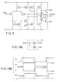
- FIG. 3 shows the first embodiment of a circuit for driving an LED by the basic rectangular voltage pulse of the present invention.
- FIG. 4 shows the second embodiment of the circuit for driving the LED by the basic rectangular voltage pulse of the present invention.
- a reference voltage is temporarily amplified by a buffer so as to hold a predetermined voltage even with a large output current load, and then the voltage is directly switched between power MOS switches Q3 and Q4 and directly output to an LED to drive the LED by the rectangular voltage pulse.
- an output circuit for driving the LED load must have an output impedance lower than Rs by one order of magnitude, e.g., 1 ⁇ or less in the above-mentioned conditions, and must have an ability capable of discharging a peak current of about 100 mA at maximum.
- FIGS. 7 to 9 show circuits which are manufactured by the Bi-CMOS process, can operate with a large amplitude even in low power supply voltage operation, and have a wide band characteristic of several hundred MHz and a high current driving ability of 100 mA or more.
- the embodiment of FIG. 7 is a high-speed buffer amplifier circuit which exploits a differential amplifier made up of bipolar transistors as an input circuit and can reduce noise with a small input/output offset voltage error.
- the maximum output voltage is limited to a voltage lower than Vdd by about 0.8V, which does not pose any problem when the LED of an n-type substrate is used by grounding the cathode.
- a problem arises when the power supply voltage for use is low and an operation condition in which the difference between Vdd and Vh is 1V or less is required.
- the lowest voltage of V1 is limited to about 1V or more.
- a differential amplifier circuit having a large in-phase input voltage allowable range is employed as the input circuit, and a pull-up circuit to Vdd is arranged in the output circuit.
- This embodiment relates to a high-speed buffer amplifier shown in FIG. 8.
- the amplifier can operate within the input range of 0V to (Vdd-0.5V).
- Vdd-0.5V P-channel MOS transistors
- a P-MOS is parallel-connected to an npn transistor on the Vdd side. After the transistor is saturated, the MOS transistor pulls up the output voltage toward Vdd, thus realizing a high speed, high current drivability, and high output voltage.
- this buffer amplifier suffers demerits such as the possibility of generating an offset error from a set input value of mV order, but can operate by fully using the voltage between Vdd and ground regardless of the input signal level, the form of the output load, and the voltage.
- the output circuits of the embodiments shown in FIGS. 7 and 8 tend to increase in high-frequency output impedance and be susceptible to noise fluctuations of a power supply or the like because the bias current of an output bipolar transistor becomes almost 0 in balanced-point operation in which the input and output are balanced.
- An embodiment of a high-speed buffer amplifier shown in FIG. 9 is designed based on that shown in FIG. 8 in order to overcome the drawback.
- This circuit is supported by high-speed pnp transistors as a process prerequisite.
- a bias current always flows through output transistors Q100 and Q101 through diodes D100 and D101 and a resistor R100, and the output circuit achieves class "AB" operation.
- the operation cutoff frequency of the output transistor can always be held around the maximum cutoff frequency of the transistor. High-frequency characteristics of the entire buffer circuit and a constant transient response regardless of operation conditions could be maintained.
- the driving circuits of the first and second embodiments require pulses Ch and Cl for controlling MOS switches, in order to sequentially switch the reference voltage by MOS switches in accordance with an externally input pulse signal Vp, sequentially control the output pulse voltage level, and obtain a rectangular voltage pulse.
- FIGS. 10A and 10B show the sequence and timing waveforms of various signals required for the control pulses.
- a circuit PG for generating the pulses Ch and Cl is constituted by a simple logical circuit shown in FIG. 10A.
- the timing waveforms of various signals and the waveform of an output voltage Vout are illustrated as ideal step responses with an added delay time on the assumption that a circuit signal delays.
- the waveform of the voltage output Vout corresponds to a chain line waveform because Vl is 0V in this embodiment.
- the forward current which exponentially increases with time along with the linear rise of the voltage, i.e., the rise operation waveform of the optical signal was quantitatively examined to find that the delay time td until the current reached 5% of the maximum current amplitude was 19.0 ns, and the time until the current reached 90% of the forward current, i.e., the rise time tr of the optical output signal intensity was 3.5 ns.
- the rise waveform of Vd is expressed by an exponential attenuation function determined by the time constant (Rs ⁇ Cd) and is asymptotic to the final value Vhigh, as shown in FIGS. 25A and 25B.
- the delay time td was 3.7 ns
- the rise time tr was 5.3 ns.
- the numerical values of the simulation results by the two different driving methods are compared to find that the time until the voltage reaches the steady-state emission level of the LED, as the sum of the delay time and rise time from the input level change start of a voltage pulse, is half or less in driving with a constant voltage pulse in comparison with driving with a constant current pulse. Constant-voltage driving is more advantageous than high-speed modulation.
- the transient response time becomes shorter, the total time until the voltage reaches a steady-state value is still 9.0 ns.
- the element capacitance Cd is halved to 100 pF, and Rs is halved to 5 ⁇ , the implementation range of an optical transmittable bit rate is limited to a medium speed range of 100 Mb/s or less.
- the low-level voltage Vl is not decreased to 0 but is always kept at a predetermined DC bias voltage.
- An embodiment of the basic circuit arrangement is almost the same as the circuit diagrams shown in FIGS. 3 and 4, and the input reference voltage Vl is set to not 0V but a predetermined DC bias voltage.
- the switch control logical circuit is also the same as those shown in FIGS. 10A and 11A, and the pulse timing waveforms are also the same as those shown in FIGS. 10B and 11B. Note that the operation waveform of the output voltage pulse Vout is higher in a low level than 0V by application of a DC bias, and corresponds to a response waveform represented by the solid line.
- a DC bias of 1.6V is applied as the Vl value.
- the input voltage changes from a high-level voltage of 2.25V to a low-level voltage of 1.6V, and the voltage across Rs is 0.65V.
- the peak value of the discharge current reaches 65 mA.
- Vl is set as high as 1.6V, a large amount of current injection can be ensured, and the fall time is as short as about 1.5 ns, as will be described later.
- the rise response changes stepwise from an input low-level voltage of 1.6V to a high-level voltage of 2.25V in pulse driving.
- the delay time td obtained by simulating the response waveform was 1.2 ns, and the rise time tr was 5.3 ns.
- the total time until the emission intensity reaches a steady-state value was 6.5 ns from the level change start of an input pulse, that was shorter by 2.5 ns as the shortened time of td than the response obtained when Vl in the initial state was set to 0V.
- the following invention is effectively applied. That is, the voltage waveform in which the high level of a pulse in constant voltage pulse driving is held at a constant single value is replaced by a binary voltage waveform in which the high level value changes midway.
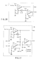
- FIG. 5 is a block diagram showing an LED driving circuit for quantifying an operation of increasing the speed as much as possible.
- the third embodiment concerns an LED driving circuit in which three reference voltages Vh2, Vh1, and Vl which define the pulse level are input and sequentially switched by small-signal MOS voltage switches Q5, Q6, and Q7, and a voltage pulse having two high level values is generated, amplified by a high-speed buffer, and output.
- the high-speed buffer amplifier at the output has already been described in detail by exemplifying the embodiments shown in FIGS. 7 to 9, and a description thereof will be omitted.
- a circuit embodiment of another driving type using a voltage pulse having two high level values is the fourth embodiment of a circuit in FIG. 6 which is similar in circuit operation to the second embodiment of single rectangular pulse driving.
- the fourth embodiment relates to an LED driving circuit in which input reference voltages Vh2, Vh1, and Vl are temporarily amplified by a buffer to enable connection to a large-current load, and these voltages are directly switched by MOS switches Q8, Q9, and Q10 to generate a binary voltage pulse.
- the two types of binary voltage pulse driving circuits adopt the same switch control.
- a necessary pulse generation logic circuit, the timing waveforms of signals, and the waveform of the output voltage Vout are shown in FIGS. 12A and 12B.
- the driving circuit for generating a binary voltage pulse switches a reference voltage source at each timing corresponding to a change in external input signal Vp, determines the pulse peak value, and shapes the pulse into a desired pulse shape.
- Vl may always be fixed as a reference, and the high level may be sequentially added as the difference from the reference voltage Vl.
- FIG. 14 shows the detailed circuit (fifth embodiment).
- a reference voltage -Vl is inversely amplified, and the reference voltage of an output Vout is always fixed to Vl.
- Difference signal voltages (Vh1-Vh2) and (Vl-Vh1) are switched by turning on/off small-signal MOS voltage switches Q11 and Q12.
- both Q11 and Q12 are off, the low level returns to only Vl.
- the output of the LED driving circuit uses an inversion/synthesis buffer amplifier.
- an initial over drive voltage (Vh2-Vh1) in high-level transition of the voltage is input from the switch as a difference from the steady-state high-level voltage Vh1.
- Vh2-Vh1 initial over drive voltage
- Vh1 initial over drive voltage
- Vh1 initial over drive voltage
- Vh1 initial over drive voltage
- Vh1 initial over drive voltage
- Vh1 initial over drive voltage in high-level transition of the voltage
- the output buffer circuit basically requires a differential input amplifier circuit.
- the differential input amplifier circuit in the circuit shown in FIG. 8 or 9 can be directly used by separating the connection of directly feeding back an output voltage to the inverting input terminal.
- the circuit is constituted to be operable by a single power supply by using different voltage addition methods and only a positive reference voltage source.
- FIG. 15 shows the sixth embodiment of an LED driving circuit designed based on this gist.
- two small-signal MOS voltage switches Q13 and Q14 and two small-signal MOS voltage switches Q15 and Q16 are attached to respective reference voltage signal lines to switch whether to input a reference voltage or to ground the line.
- This circuit is based on the circuit operation principle in which Vout is a voltage prepared by always adding and averaging a total of three voltages at a Vl input terminal and two input terminals after the switches.
- FIG. 16A shows the timing waveforms of respective signals and the waveform of the output voltage Vout at the same time.
- the response waveform when the LED was driven by a voltage pulse having two high level values by using any one of the circuits in the third to sixth embodiments was quantitatively analyzed.
- the initial peak voltage Vh2 at the pulse leading edge was set to 2.6V and the subsequent steady-state level voltage Vh1 was set to 2.25V, i.e., when the initial high level value at the pulse rise was set higher by 0.35V than the single-value peak voltage of 2.25V, the delay time was 0.71 ns and the rise time was 1.25 ns.
- the time until the emission intensity reached the steady-state value was greatly shortened to 1.96 ns.
- the instantaneous peak current at the leading edge reached 100 mA, which is five times a steady-state driving current If of 20 mA.
- An impulse-shaped current of 100 mA is injected in transmitting a signal of an arbitrary pattern, and the circuit operation must be so designed as to cope with impulse operation.
- this value does not obstruct implementation.
- the fall time of an optical output pulse at this time was checked to be 1.51 ns. This value is almost equal to a rise time of 1.25 ns in driving with a constant voltage pulse having two high level values, and indicates a transmission possibility of several hundred Mb/s.
- the fall time can be shortened to almost 0.5 ns, which results in unbalanced fall and rise times and does not contribute to an increase in speed.
- the rise delay time with respect to an electrical pulse is only about 0.1 ns.
- the delay time is shortened to about 0.7 ns, which cannot be ignored.
- the pulse width of an output optical signal including rise/fall correction is smaller by about 0.5 ns than the width of the externally input signal pulse Vp. If a high-speed element can be similarly used and either of the element constants Rs and Cd of the LED can be halved, the above-described LED driving circuit of the present invention can be applied to realize an optical data link having a maximum transfer rate of 500 Mb/s.
- the prospective pulse width narrowing amount at this time is 0.25 ns.
- the pulse narrowing phenomenon that the pulse width of an LED output optical signal decreases occurs more or less in principle. If this narrowing amount changes the duty ratio or appears as a time jitter in signal transmission, the pulse narrowing phenomenon can. be prevented by applying the present invention of compensating for a high-pulse width by a pulse narrowing amount generated by the driving method. That is, a circuit of increasing the high-pulse width of an input signal by a pulse narrowing amount in advance is added to widen the LED driving voltage pulse.
- the basic operation principle of a driving circuit for realizing this can be achieved by changing only the control pulse generation circuit in each of the circuits in the first to sixth embodiments.
- the function which should be included in the control pulse generation circuit is an operation function of generating a sequential pulse whose high-level pulse width is increased by the narrowing amount by using a combination of two delay circuits and a logic synthesis circuit at maximum on the basis of a pulse prepared by temporarily shaping an externally input signal waveform into an appropriate rectangular waveform.
- the arrangement of the switch-controlled pulse generation logic circuit is changed in accordance with the voltage pulse generation method.
- FIG. 11A shows a detailed input signal pulse Vp, the sequence waveforms of control pulses Cl and Ch whose pulse widths are increased, and the waveform of the output voltage Vout.
- FIG. 13A shows a switch-controlled pulse generation logic circuit using the binary voltage pulse driving circuit method that can be applied to the third and fourth embodiments.
- FIG. 13B shows the timing waveforms of various signals used in the circuit of FIG. 13A.
- the high-pulse width of the driving voltage pulse Vout is increased by a combination of Ch1 and Cl whose pulse widths are increased and Ch2 whose pulse width is kept unchanged.
- FIGS. 17A and 17B show a switch-controlled pulse generation logic circuit and the timing waveforms of signals which can be applied to the fifth and sixth embodiments that employ the same binary voltage pulse driving method but different circuit arrangements.
- the pulse width of only the control pulse Cl is increased without changing that of the control pulse Ch, thus obtaining the driving voltage pulse Vout whose high-pulse width is increased.
- the narrowing amount of the high-level width is 0.5 ns, so that the optical value of the pulse width increase to be set in the logical synthesis circuit is 0.5 ns.
- the narrowing amount can be satisfactorily compensated for by substantially increasing the pulse width by 2 ns or less.
- the signal delay circuit necessary for the pulse width increase can be small in circuit size, and can be compactly assembled in an IC chip.
- the LED driving circuit itself can be assembled in a small-size one-chip IC.
- the LED driving circuit can be applied to realize an optical data link having a transmission rate up to about 500 Mb/s.
- the LED driving circuit of the present invention can realize a sub-Gbit-rate optical data link using an LED with a minimum increase in power consumption and low cost.
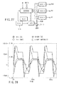
- FIG. 28 shows the results of analyzing the voltage/current operation waveform and output optical signal waveform of an LED in binary voltage pulse driving by using an actual LED diode model described by full parameters almost similar to the electrical characteristics of the LED employed as a typical example.
- FIG. 28 shows characteristics for a repetitive signal of 250 Mb/s.
- a finite transient response pulse different from an ideal rectangular pulse suppresses the peak current in a transient response
- the optical output waveform attains a proper pulse shape which keeps a duty ratio of 2 : 1. It can be easily estimated that transmission at 500 Mb/s or more is enabled by exchanging the LED for one improved in characteristics so as to cope with high speed, and optimizing driving conditions.
- a red LED has a larger band gap than that of an Si diode, but is essentially a diode.
- a forward voltage Vf necessary for flowing a forward current of a predetermined value has a large temperature dependence unique to the diode upon a change in operation temperature, similar to the Si diode.
- N is a parameter which determines the magnitude of the temperature dependence regardless of the element material. N depends on the device, and when a current necessary for emission of the LED actually flows, the diode is in an operation region where the voltage drop at Rs cannot be ignored. From this, the diode behaves out of a simple ideal operation state. By selecting operation conditions, the temperature dependence of the LED exhibits almost the same characteristic as that of the Si diode. Even if their characteristics are different, the difference falls within several tens of %.
- the driving voltage level Vf applied to the current is made to follow the temperature change.
- a circuit is so designed as to be able to always generate, controlled low-level voltage Vl of the DC bias voltage which guarantees high-speed operation of the LED and Vh which determines an optical output intensity, following a temperature change in the forward voltage of the LED.
- FIGS. 18 to 20 show detailed examples of the basic arrangement of a reference voltage generation circuit which matches this purpose.
- a stabilization constant current source I1 using a band gap reference voltage as a reference is used to generate a DC current independent of the temperature.
- Resistors R51, R52, and R53 and an Si diode Si ⁇ D having forward voltage dependence corresponding to the temperature change amount of the LED are selected and cascade-connected to obtain three reference voltages Vl, Vh1, and Vh2.
- the resistance value can be uniquely determined by a DC current value in use, a corresponding forward voltage of Si ⁇ D, and three reference voltages to be generated.
- the reference voltage generation circuit is used for direct reference voltage generation of an LED having the same characteristics as those of an LED used for photoelectric conversion.
- a DC current generated by a constant current source I1 is set equal to a current flowing for a low-level signal when the LED is OFF.
- the resistance values of R54 and R55 are determined to generate voltage differences (Vh1-V1) and (Vh2-V2) on the basis of the current value.
- the embodiment of FIG. 20 concerns a circuit using an Si ⁇ D element having a stabilization reference voltage Vref and the same temperature dependence as that of an LED, and two feedback amplifiers which need not have very-high-frequency characteristics.
- a bias current flowing through Si ⁇ D is given by Vref/R10.
- the circuit temporarily generates Vl and then generates Vh based on Vl.
- the output voltages Vl and Vh can be respectively adjusted by grounded R10 and R14, and the circuit can be easily changed in structure to adjust Vl and Vh from the outside of the IC.
- To generate a voltage Vh2, a circuit identical to one for generating Vh1 Vh is added. This embodiment is shown in FIG. 23.
- the emission efficiency of an LED has a negative temperature coefficient.
- a positive temperature coefficient can be substantially set to a high current value with respect to a temperature change by setting the temperature coefficient smaller than Vf, and a decrease in optical output pulse amplitude along with temperature rise can also be compensated for.
- FIG. 21 shows an embodiment having this function as a modification of the embodiment in FIG. 20.
- a stabilization voltage is temporarily generated to meet a voltage difference (Vh-Vl) at room temperature, and the sum of the stabilization voltage and Vl is calculated to generate Vh.
- Vh is a voltage having a predetermined voltage difference from Vl independently of the temperature.
- Each of the above-described circuits uses a single LED for a voltage reference, or selects an Si diode having the same radiation coefficient N as that of the LED and uses the Si diode for a voltage reference.
- the circuit generates the reference voltages Vl, and Vh or Vh1 and Vh2 while compensating for temperature dependence.
- FIG. 22 shows a circuit example which implements this.
- the method of fixing circuit constants in the IC cannot cope with flexible applications to various LEDs in order to use the LED driving circuit as a general-purpose component.
- temperature characteristic data of the forward voltage of a diode in the IC process which uses temperature characteristic data of an LED used in an EEPROM are written/held, the forward voltage of the Si diode on the IC substrate is converted into EEPROM address data by an A/D converter, and output data from the EEPROM is input to a D/A converter to generate a follow-up voltage.
- the block diagram of this is a temperature-compensated reference voltage generation circuit constituted by a combination of an EEPROM and D/A converters shown in FIG. 27.
- Write data Data is written in the EEPROM in advance under the control of a terminal W.
- digital data to three D/A converters are refreshed by a control circuit Ctrl at a timing based on the internal clock of an LED driver circuit or an externally input clock Clk.
- an intensity monitor photodetector is arranged near the LED as a means for more positively keeping an optical signal constant, and a feedback circuit for controlling the voltage of a driving voltage pulse so as to maintain the average output of the intensity monitor signal at a predetermined value is arranged.
- a feedback circuit for controlling the voltage of a driving voltage pulse so as to maintain the average output of the intensity monitor signal at a predetermined value is arranged.
- the LED driving circuit according to the present invention has been exemplified.
- FIG. 29 is a perspective view showing the schematic arrangement of the main part of the optical transmitting/receiving module according to the present invention.
- the use of the above-described driving circuit can implement a transmitting module which can perform high-speed modulation for an LED essentially having a large junction capacitance, is small in pulse waveform distortion, and can cope with a low-voltage power supply with low power consumption.
- the module shown in FIG. 29 comprises an IC 1 in which the LED driving circuit of the present invention is assembled, an LED element 2, and a capacitor 9 and resistor 10 accessory to operating the module. These components are mounted at once as a submodule on a submodule substrate 4 or plastic mold lead frame.
- the module has a molded optical connector 5 in order to couple an LED on the module to an optical waveguide such as a plastic fiber.
- Leads 6 for electrically coupling the module to the outside are attached to one end of the module.
- the module is molded by a plastic package 7.
- leads are attached to only one end of the module.
- lead-attaching portions can be appropriately selected, and leads may be attached to the other end of the package.
- leads for ensuring the mechanical strength in mounting the module on a printed board may be attached.
- a transceiver module structure constituted by mounting a receiving module parallel to the transmitting module and integrating them also falls within the spirit and scope of the present invention.
- FIG. 29 shows an example of the optical transmitting/receiving module which incorporates a photodetector 3 and reception IC 8.
- the present invention can implement a compact optical connector-coupled plastic transmitting module or optical transmitting/receiving module which operates by a single power supply with low power consumption and can be used in a normal heat dissipation design.
- the optical element driving circuit of the present invention using the Bi-CMOS process have been described.
- the present invention is not limited to them.
- the circuit must be modified in accordance with the characteristics of a transistor element adopted to constitute a concrete circuit.
- a transistor element other than a Bi-CMOS, such as an Si bipolar transistor or CMOS element is applied, an optical semiconductor element driving circuit which operates similarly in principle is implemented without departing from the spirit and scope of the present invention.
- the present invention high-speed modulation is realized by using an LED which cannot be driven at a high speed in the prior art.
- the distortion of an output optical pulse waveform can be reduced, an increase in power consumption can be minimized, and all circuits can be mounted compactly in an IC.
- the present invention can implement an LED driving circuit which can be easily assembled in a one-chip IC and can operate even on a low-voltage power supply.
- the present invention can provide a compact optical connector-coupled plastic optical transmitting module which operates at low power consumption on a power supply voltage from a single power supply shared by another signal processing IC and can be used in a normal heat dissipation design.
Landscapes
- Engineering & Computer Science (AREA)
- Physics & Mathematics (AREA)
- Electromagnetism (AREA)
- Computer Networks & Wireless Communication (AREA)
- Signal Processing (AREA)
- Computer Hardware Design (AREA)
- General Physics & Mathematics (AREA)
- Theoretical Computer Science (AREA)
- Led Devices (AREA)
- Optical Communication System (AREA)
- Electronic Switches (AREA)
Applications Claiming Priority (2)
| Application Number | Priority Date | Filing Date | Title |
|---|---|---|---|
| JP2000143530A JP2001326569A (ja) | 2000-05-16 | 2000-05-16 | Led駆動回路及び光送信モジュール |
| JP2000143530 | 2000-05-16 |
Publications (2)
| Publication Number | Publication Date |
|---|---|
| EP1156603A2 true EP1156603A2 (fr) | 2001-11-21 |
| EP1156603A3 EP1156603A3 (fr) | 2005-04-20 |
Family
ID=18650340
Family Applications (1)
| Application Number | Title | Priority Date | Filing Date |
|---|---|---|---|
| EP01111278A Withdrawn EP1156603A3 (fr) | 2000-05-16 | 2001-05-16 | Circuit de commande d'une diode electroluminescente et module d'émission optique |
Country Status (6)
| Country | Link |
|---|---|
| US (1) | US6724376B2 (fr) |
| EP (1) | EP1156603A3 (fr) |
| JP (1) | JP2001326569A (fr) |
| KR (1) | KR100396724B1 (fr) |
| CN (1) | CN1248434C (fr) |
| TW (1) | TW483203B (fr) |
Cited By (4)
| Publication number | Priority date | Publication date | Assignee | Title |
|---|---|---|---|---|
| DE8902725U1 (fr) * | 1989-03-07 | 1989-07-06 | Ucosan B.V., Roden, Nl | |
| EP1401127A2 (fr) * | 2002-09-18 | 2004-03-24 | Pioneer Corporation | Dispositif de modulation |
| EP1629979A1 (fr) * | 2003-06-04 | 2006-03-01 | Mimaki Engineering Co., Ltd. | Imprimante jets d'encre utilisant de l'encre uv |
| CN103928841A (zh) * | 2014-04-16 | 2014-07-16 | 中国科学院上海微系统与信息技术研究所 | 一种太赫兹量子级联激光器的高速调制方法及装置 |
Families Citing this family (101)
| Publication number | Priority date | Publication date | Assignee | Title |
|---|---|---|---|---|
| JP3508704B2 (ja) * | 2000-07-26 | 2004-03-22 | 日本電気株式会社 | 光送信回路 |
| JP3456987B2 (ja) * | 2001-12-07 | 2003-10-14 | 松下電器産業株式会社 | 光送信装置 |
| EP1461631B1 (fr) * | 2001-12-19 | 2007-06-06 | Koninklijke Philips Electronics N.V. | Procede et dispositif de remedier a des defauts de faible resistivite dans un ecran plat |
| US7215886B2 (en) * | 2002-02-04 | 2007-05-08 | Hitachi, Ltd. | Optical communication module |
| DE10225670A1 (de) * | 2002-06-10 | 2003-12-24 | Patent Treuhand Ges Fuer Elektrische Gluehlampen Mbh | Ansteuerschaltung für mindestens einen LED-Strang |
| JP3835363B2 (ja) * | 2002-07-09 | 2006-10-18 | 株式会社デンソー | 車両用発電制御装置 |
| KR20040014014A (ko) * | 2002-08-09 | 2004-02-14 | 주식회사 케이이씨 | 광 송신용 집적회로 |
| KR100474706B1 (ko) * | 2002-09-11 | 2005-03-10 | 삼성전자주식회사 | 통신시스템에서 티씨피/아이피를 이용한 프로세서 간 통신장치 |
| JP4017960B2 (ja) * | 2002-10-24 | 2007-12-05 | 日本テキサス・インスツルメンツ株式会社 | 駆動回路 |
| JP2004235498A (ja) * | 2003-01-31 | 2004-08-19 | Anden | 発光ダイオードの制御装置 |
| US7170335B2 (en) * | 2004-03-08 | 2007-01-30 | Avago Technologies Ecbu Ip (Singapore) Pte. Ltd. | Driver circuit for driving a light source of an optical pointing device |
| US7499003B2 (en) * | 2004-03-31 | 2009-03-03 | Electrolux Home Products, Inc. | Disappearing interface system |
| US6972530B1 (en) * | 2004-04-05 | 2005-12-06 | National Semiconductor Corporation | Apparatus and method for transparent dynamic range scaling for open loop LED drivers |
| US7646029B2 (en) * | 2004-07-08 | 2010-01-12 | Philips Solid-State Lighting Solutions, Inc. | LED package methods and systems |
| JP4170963B2 (ja) * | 2004-07-22 | 2008-10-22 | 浜松ホトニクス株式会社 | Led駆動回路 |
| JP4224001B2 (ja) * | 2004-07-22 | 2009-02-12 | 浜松ホトニクス株式会社 | Led駆動回路 |
| US8733966B2 (en) | 2004-08-20 | 2014-05-27 | Mag Instrument, Inc. | LED flashlight |
| JP4566692B2 (ja) * | 2004-10-28 | 2010-10-20 | シャープ株式会社 | 発光ダイオード駆動装置及びそれを備えた光伝送装置 |
| KR100885573B1 (ko) * | 2004-12-27 | 2009-02-24 | 교세라 가부시키가이샤 | 화상 표시 장치 및 그 구동 방법, 및 전자 기기의 구동방법 |
| US7453306B2 (en) * | 2005-11-07 | 2008-11-18 | Jds Uniphase Corporation | Pulse shaping circuit |
| US7621655B2 (en) * | 2005-11-18 | 2009-11-24 | Cree, Inc. | LED lighting units and assemblies with edge connectors |
| US7400310B2 (en) * | 2005-11-28 | 2008-07-15 | Draeger Medical Systems, Inc. | Pulse signal drive circuit |
| US7592754B2 (en) * | 2006-03-15 | 2009-09-22 | Cisco Technology, Inc. | Method and apparatus for driving a light emitting diode |
| JP2012034417A (ja) * | 2006-06-20 | 2012-02-16 | Panasonic Corp | パルス変調回路及びパルス変調方法 |
| JP4982260B2 (ja) | 2006-06-20 | 2012-07-25 | パナソニック株式会社 | パルス変調回路 |
| TWI340370B (en) * | 2006-08-24 | 2011-04-11 | Chimei Innolux Corp | System for displaying image |
| KR101152445B1 (ko) | 2006-08-31 | 2012-06-01 | 삼성모바일디스플레이주식회사 | 발광제어구동부 및 그를 이용한 유기전계발광표시장치 |
| KR100811988B1 (ko) | 2006-08-31 | 2008-03-10 | 삼성에스디아이 주식회사 | 발광제어구동부, 발광제어신호 구동방법 및 그를 이용한유기전계발광표시장치 |
| KR100873072B1 (ko) | 2006-08-31 | 2008-12-09 | 삼성모바일디스플레이주식회사 | 발광제어구동부 및 그를 이용한 유기전계발광표시장치 |
| CN100583771C (zh) * | 2006-10-11 | 2010-01-20 | 鸿富锦精密工业(深圳)有限公司 | 网络状态指示电路 |
| US7917040B2 (en) | 2006-11-08 | 2011-03-29 | Electronics & Telecommunications Research Institute | Method and apparatus for controlling wavelength tuning of optical source for optical communication |
| KR100856923B1 (ko) * | 2006-11-08 | 2008-09-05 | 한국전자통신연구원 | 광통신 시스템에서의 광원 파장 가변 제어 방법 및 장치 |
| CN101589647B (zh) * | 2007-01-22 | 2012-12-12 | 皇家飞利浦电子股份有限公司 | 有机发光二极管结构 |
| DE102007004393A1 (de) * | 2007-01-29 | 2008-07-31 | Patent-Treuhand-Gesellschaft für elektrische Glühlampen mbH | Ansteuerschaltung und Verfahren zur Ansteuerung von großflächigen Halbleiterlichtquellen |
| JP2008271503A (ja) * | 2007-03-26 | 2008-11-06 | Matsushita Electric Ind Co Ltd | 参照電流回路 |
| JP5201874B2 (ja) * | 2007-05-14 | 2013-06-05 | キヤノン株式会社 | 画像形成装置 |
| EP2160927B1 (fr) * | 2007-06-19 | 2021-04-14 | Silicon Line GmbH | Circuiterie et procédé pour commander des composants électroluminescents |
| WO2008155384A1 (fr) * | 2007-06-19 | 2008-12-24 | Silicon Line Gmbh | Circuiterie et procédé pour commander des composants électroluminescents |
| US7598683B1 (en) | 2007-07-31 | 2009-10-06 | Lsi Industries, Inc. | Control of light intensity using pulses of a fixed duration and frequency |
| US8903577B2 (en) | 2009-10-30 | 2014-12-02 | Lsi Industries, Inc. | Traction system for electrically powered vehicles |
| US8604709B2 (en) | 2007-07-31 | 2013-12-10 | Lsi Industries, Inc. | Methods and systems for controlling electrical power to DC loads |
| DE102008003089A1 (de) * | 2007-08-06 | 2009-02-26 | Siemens Ag | Datenübertragungssystem und Verfahren zum Übertragen von Daten in einem Datenübertragungssystem |
| CN101431446B (zh) * | 2007-11-09 | 2012-05-23 | 鸿富锦精密工业(深圳)有限公司 | 网络状态指示电路 |
| CN101453270B (zh) * | 2007-12-04 | 2013-04-24 | 无锡江南计算技术研究所 | 激光驱动器及其温度补偿电路 |
| US8115419B2 (en) * | 2008-01-23 | 2012-02-14 | Cree, Inc. | Lighting control device for controlling dimming, lighting device including a control device, and method of controlling lighting |
| US8278831B2 (en) * | 2008-01-28 | 2012-10-02 | Nxp B.V. | LED driver circuit and method, and system and method for estimating the junction temperature of a light emitting diode |
| JP5130975B2 (ja) * | 2008-03-19 | 2013-01-30 | 富士通株式会社 | 光スイッチ駆動回路 |
| US9153297B2 (en) * | 2008-04-03 | 2015-10-06 | Infineon Technologies Ag | Integrated circuit and method for manufacturing the same |
| JP5489180B2 (ja) * | 2008-05-21 | 2014-05-14 | シリコン・ライン・ゲー・エム・ベー・ハー | 発光コンポーネントを制御するための回路構造と方法 |
| JP5151695B2 (ja) * | 2008-05-29 | 2013-02-27 | 富士通株式会社 | 駆動回路および光スイッチ |
| JP5176799B2 (ja) * | 2008-09-08 | 2013-04-03 | 船井電機株式会社 | レーザ駆動回路及びレーザディスプレイ |
| JP5161176B2 (ja) * | 2008-09-26 | 2013-03-13 | 太陽誘電株式会社 | 可視光通信用送信機及び可視光通信システム |
| WO2010040816A2 (fr) | 2008-10-09 | 2010-04-15 | Silicon Line Gmbh | Circuit et procédé de transmission de signaux codés tmds |
| US20120091816A1 (en) * | 2010-11-15 | 2012-04-19 | O2Micro, Inc. | Power systems with multiple power sources |
| US8508142B2 (en) | 2009-03-20 | 2013-08-13 | O2Micro Inc. | Portable lighting device and method thereof |
| US8217591B2 (en) * | 2009-05-28 | 2012-07-10 | Cree, Inc. | Power source sensing dimming circuits and methods of operating same |
| JP4879369B2 (ja) * | 2009-08-24 | 2012-02-22 | 三菱電機株式会社 | 光送信器の誤発光防止回路 |
| US10264637B2 (en) | 2009-09-24 | 2019-04-16 | Cree, Inc. | Solid state lighting apparatus with compensation bypass circuits and methods of operation thereof |
| US9713211B2 (en) * | 2009-09-24 | 2017-07-18 | Cree, Inc. | Solid state lighting apparatus with controllable bypass circuits and methods of operation thereof |
| US8901845B2 (en) | 2009-09-24 | 2014-12-02 | Cree, Inc. | Temperature responsive control for lighting apparatus including light emitting devices providing different chromaticities and related methods |
| US9285103B2 (en) | 2009-09-25 | 2016-03-15 | Cree, Inc. | Light engines for lighting devices |
| US9464801B2 (en) | 2009-09-25 | 2016-10-11 | Cree, Inc. | Lighting device with one or more removable heat sink elements |
| US9068719B2 (en) * | 2009-09-25 | 2015-06-30 | Cree, Inc. | Light engines for lighting devices |
| US9353933B2 (en) * | 2009-09-25 | 2016-05-31 | Cree, Inc. | Lighting device with position-retaining element |
| US8602579B2 (en) * | 2009-09-25 | 2013-12-10 | Cree, Inc. | Lighting devices including thermally conductive housings and related structures |
| US8777449B2 (en) | 2009-09-25 | 2014-07-15 | Cree, Inc. | Lighting devices comprising solid state light emitters |
| US20110081945A1 (en) * | 2009-10-06 | 2011-04-07 | Microvision, Inc. | High Efficiency Laser Drive Apparatus |
| US9217542B2 (en) | 2009-10-20 | 2015-12-22 | Cree, Inc. | Heat sinks and lamp incorporating same |
| US9030120B2 (en) * | 2009-10-20 | 2015-05-12 | Cree, Inc. | Heat sinks and lamp incorporating same |
| CN102076141A (zh) * | 2009-11-21 | 2011-05-25 | 佛山市顺德区汉达精密电子科技有限公司 | 发光二极管驱动电路 |
| US9518715B2 (en) * | 2010-02-12 | 2016-12-13 | Cree, Inc. | Lighting devices that comprise one or more solid state light emitters |
| CN102844619B (zh) | 2010-02-12 | 2016-12-28 | 科锐公司 | 具有散热件的照明设备 |
| KR20120128139A (ko) | 2010-02-12 | 2012-11-26 | 크리, 인코포레이티드 | 하나 이상의 고체 상태 발광기를 포함하는 조명 장치 |
| US9175811B2 (en) | 2010-02-12 | 2015-11-03 | Cree, Inc. | Solid state lighting device, and method of assembling the same |
| US8773007B2 (en) | 2010-02-12 | 2014-07-08 | Cree, Inc. | Lighting devices that comprise one or more solid state light emitters |
| US8476836B2 (en) | 2010-05-07 | 2013-07-02 | Cree, Inc. | AC driven solid state lighting apparatus with LED string including switched segments |
| JP5842090B2 (ja) * | 2010-08-25 | 2016-01-13 | パナソニックIpマネジメント株式会社 | 照明光通信装置 |
| US10030863B2 (en) | 2011-04-19 | 2018-07-24 | Cree, Inc. | Heat sink structures, lighting elements and lamps incorporating same, and methods of making same |
| US9839083B2 (en) | 2011-06-03 | 2017-12-05 | Cree, Inc. | Solid state lighting apparatus and circuits including LED segments configured for targeted spectral power distribution and methods of operating the same |
| US9510413B2 (en) | 2011-07-28 | 2016-11-29 | Cree, Inc. | Solid state lighting apparatus and methods of forming |
| US8742671B2 (en) | 2011-07-28 | 2014-06-03 | Cree, Inc. | Solid state lighting apparatus and methods using integrated driver circuitry |
| JP5333569B2 (ja) * | 2011-12-12 | 2013-11-06 | 日本テキサス・インスツルメンツ株式会社 | 発光ダイオード制御装置 |
| JP5762943B2 (ja) * | 2011-12-27 | 2015-08-12 | 株式会社東芝 | 光送受信回路装置及び受信回路 |
| CN102573235B (zh) | 2012-01-11 | 2013-07-24 | 矽力杰半导体技术(杭州)有限公司 | 一种高效率的led驱动电路及其驱动方法 |
| US9554445B2 (en) | 2012-02-03 | 2017-01-24 | Cree, Inc. | Color point and/or lumen output correction device, lighting system with color point and/or lumen output correction, lighting device, and methods of lighting |
| US10378749B2 (en) | 2012-02-10 | 2019-08-13 | Ideal Industries Lighting Llc | Lighting device comprising shield element, and shield element |
| US9155140B2 (en) | 2012-06-07 | 2015-10-06 | Gabriel Yavor | Optical waveform generator |
| JP5579804B2 (ja) | 2012-08-28 | 2014-08-27 | ミネベア株式会社 | 負荷駆動装置およびその制御方法 |
| DE102012113024A1 (de) * | 2012-12-21 | 2014-06-26 | Hamilton Bonaduz Ag | Optische Messvorrichtung |
| TWI516028B (zh) | 2013-06-20 | 2016-01-01 | 財團法人工業技術研究院 | 高低壓隔離內埋功率模組 |
| CN104078018B (zh) * | 2014-07-15 | 2016-09-21 | 苏州华兴源创电子科技有限公司 | 一种全高清液晶阵列驱动电路 |
| US9705601B2 (en) * | 2014-11-28 | 2017-07-11 | Sumitomo Electric Industries, Ltd. | Driver for pulse amplitude modulation and optical transmitter implementing the same |
| JP6324340B2 (ja) * | 2015-03-27 | 2018-05-16 | アズビル株式会社 | 光電センサ |
| TWI564867B (zh) * | 2016-03-18 | 2017-01-01 | 明陽半導體股份有限公司 | 發光二極體驅動電路及方法 |
| ES2701334T3 (es) * | 2016-08-01 | 2019-02-21 | Knowledge Dev For Pof Sl | Controlador LED para comunicaciones ópticas de alta velocidad en base a modulaciones lineales |
| CN107592163B (zh) * | 2017-09-11 | 2020-04-24 | 东南大学 | 光通信系统中的最佳led串联数量的确定方法 |
| US10295909B2 (en) * | 2017-09-26 | 2019-05-21 | Taiwan Semiconductor Manufacturing Co., Ltd. | Edge-exposure tool with an ultraviolet (UV) light emitting diode (LED) |
| CN110119179B (zh) * | 2019-05-08 | 2020-08-07 | 思瑞浦微电子科技(苏州)股份有限公司 | 应用于多高压源的浮动高压选择电路 |
| CN112018596A (zh) * | 2019-05-31 | 2020-12-01 | 宁波飞芯电子科技有限公司 | 一种辐射驱动电路、辐射驱动方法及辐射发射装置 |
| CN113131920B (zh) * | 2021-04-09 | 2023-05-09 | 成都芯源系统有限公司 | 快速低偏置电压的双向缓冲器 |
| JP7405885B2 (ja) | 2022-03-04 | 2023-12-26 | 菊水電子工業株式会社 | 同期整流回路 |
Citations (4)
| Publication number | Priority date | Publication date | Assignee | Title |
|---|---|---|---|---|
| US3968399A (en) * | 1975-03-19 | 1976-07-06 | The United States Of America As Represented By The Secretary Of The Navy | Method for driving a LED at high speed |
| US4571506A (en) * | 1984-03-28 | 1986-02-18 | At&T Bell Laboratories | LED Driver Circuit |
| EP0469244A2 (fr) * | 1990-08-02 | 1992-02-05 | Sumitomo Electric Industries, Ltd. | Circuit de commande d'un élément émetteur de lumière |
| US5883910A (en) * | 1997-07-03 | 1999-03-16 | Maxim Integrated Products, Inc. | High speed semiconductor laser driver circuits |
Family Cites Families (12)
| Publication number | Priority date | Publication date | Assignee | Title |
|---|---|---|---|---|
| EP0101872B1 (fr) | 1982-07-19 | 1990-01-03 | Kabushiki Kaisha Toshiba | Module de communication optique bidirectionnelle |
| JPS6259914A (ja) | 1985-09-10 | 1987-03-16 | Fuji Photo Optical Co Ltd | 内視鏡 |
| CA2048198C (fr) * | 1990-08-09 | 1996-06-04 | Kai Y. Eng | Commutation modulaire |
| US5343323A (en) * | 1991-10-24 | 1994-08-30 | General Motors Corporation | Lan electro-optical interface |
| IT1268070B1 (it) * | 1994-06-06 | 1997-02-20 | Cselt Centro Studi Lab Telecom | Circuito in tecnologia cmos per il pilotaggo ad alta velocita' di sorgenti ottiche. |
| SE504326C2 (sv) * | 1995-05-17 | 1997-01-13 | Ericsson Telefon Ab L M | Anordningar avseende ljusemitterande organ |
| JP3340345B2 (ja) | 1997-03-26 | 2002-11-05 | 株式会社東芝 | 定電圧発生回路 |
| JP4116133B2 (ja) | 1997-07-31 | 2008-07-09 | 株式会社東芝 | 温度依存型定電流発生回路およびこれを用いた光半導体素子の駆動回路 |
| JP3732345B2 (ja) * | 1998-02-10 | 2006-01-05 | 株式会社沖データ | 駆動回路、ledヘッド及びプリンタ |
| JP3668612B2 (ja) | 1998-06-29 | 2005-07-06 | 株式会社東芝 | 光半導体素子駆動回路及び光送受信モジュール |
| JP4026970B2 (ja) | 1999-02-05 | 2007-12-26 | シャープ株式会社 | 発光ダイオードの駆動方法およびそれを用いた光伝送装置 |
| JP4116198B2 (ja) | 1999-06-29 | 2008-07-09 | 株式会社東芝 | 光半導体素子駆動回路及び光送受信モジュール |
-
2000
- 2000-05-16 JP JP2000143530A patent/JP2001326569A/ja active Pending
-
2001
- 2001-05-01 TW TW090110434A patent/TW483203B/zh not_active IP Right Cessation
- 2001-05-16 CN CNB011178000A patent/CN1248434C/zh not_active Expired - Fee Related
- 2001-05-16 KR KR10-2001-0026771A patent/KR100396724B1/ko not_active IP Right Cessation
- 2001-05-16 EP EP01111278A patent/EP1156603A3/fr not_active Withdrawn
- 2001-05-16 US US09/858,757 patent/US6724376B2/en not_active Expired - Lifetime
Patent Citations (4)
| Publication number | Priority date | Publication date | Assignee | Title |
|---|---|---|---|---|
| US3968399A (en) * | 1975-03-19 | 1976-07-06 | The United States Of America As Represented By The Secretary Of The Navy | Method for driving a LED at high speed |
| US4571506A (en) * | 1984-03-28 | 1986-02-18 | At&T Bell Laboratories | LED Driver Circuit |
| EP0469244A2 (fr) * | 1990-08-02 | 1992-02-05 | Sumitomo Electric Industries, Ltd. | Circuit de commande d'un élément émetteur de lumière |
| US5883910A (en) * | 1997-07-03 | 1999-03-16 | Maxim Integrated Products, Inc. | High speed semiconductor laser driver circuits |
Cited By (8)
| Publication number | Priority date | Publication date | Assignee | Title |
|---|---|---|---|---|
| DE8902725U1 (fr) * | 1989-03-07 | 1989-07-06 | Ucosan B.V., Roden, Nl | |
| EP1401127A2 (fr) * | 2002-09-18 | 2004-03-24 | Pioneer Corporation | Dispositif de modulation |
| EP1401127A3 (fr) * | 2002-09-18 | 2005-04-06 | Pioneer Corporation | Dispositif de modulation |
| EP1629979A1 (fr) * | 2003-06-04 | 2006-03-01 | Mimaki Engineering Co., Ltd. | Imprimante jets d'encre utilisant de l'encre uv |
| EP1629979A4 (fr) * | 2003-06-04 | 2006-06-21 | Mimaki Eng Kk | Imprimante jets d'encre utilisant de l'encre uv |
| US7690781B2 (en) | 2003-06-04 | 2010-04-06 | Mimaki Engineering Co., Ltd. | Ink jet printer using UV ink |
| CN103928841A (zh) * | 2014-04-16 | 2014-07-16 | 中国科学院上海微系统与信息技术研究所 | 一种太赫兹量子级联激光器的高速调制方法及装置 |
| CN103928841B (zh) * | 2014-04-16 | 2017-06-06 | 中国科学院上海微系统与信息技术研究所 | 一种太赫兹量子级联激光器的高速调制方法及装置 |
Also Published As
| Publication number | Publication date |
|---|---|
| CN1324153A (zh) | 2001-11-28 |
| CN1248434C (zh) | 2006-03-29 |
| JP2001326569A (ja) | 2001-11-22 |
| KR100396724B1 (ko) | 2003-09-02 |
| US6724376B2 (en) | 2004-04-20 |
| TW483203B (en) | 2002-04-11 |
| EP1156603A3 (fr) | 2005-04-20 |
| US20010043093A1 (en) | 2001-11-22 |
| KR20010105228A (ko) | 2001-11-28 |
Similar Documents
| Publication | Publication Date | Title |
|---|---|---|
| US6724376B2 (en) | LED driving circuit and optical transmitting module | |
| EP0895325B1 (fr) | Alimentation de courant de valeur constante dépendant de la température et circuit d'alimentation d'un dispositif semiconducteur à l'emission de la lumière | |
| KR101965788B1 (ko) | 단일 종단형 구성가능한 다중 모드 드라이버 | |
| US7269194B2 (en) | High speed laser array driver | |
| US5914622A (en) | Pulse-width controller | |
| EP2112727B1 (fr) | Pilote couplé en CC doté d'une terminaison active | |
| US7154923B2 (en) | Method and apparatus for providing a modulation current | |
| IL133819A (en) | Fast semiconductor laser driving circuits | |
| US6031855A (en) | Light emitting element driving circuit and light emitting device having the same | |
| US6922045B2 (en) | Current driver and method of precisely controlling output current | |
| EP1803222A2 (fr) | Etage de sortie haute vitesse et basse tension pour pilote de laser ou de modulateur | |
| KR100389921B1 (ko) | 원칩으로 구현되며 고속으로 동작하는 광 수신 장치 | |
| JP4116198B2 (ja) | 光半導体素子駆動回路及び光送受信モジュール | |
| JP2000244251A (ja) | 補償回路 | |
| US6606177B1 (en) | Driver circuit and optical-transmission module | |
| US5391933A (en) | Driver circuit for generating pulses | |
| US6922075B1 (en) | Low power driver circuitry | |
| KR100810328B1 (ko) | 전류 구동형 광원 구동 회로 | |
| Chen et al. | A 2.5 Gbps CMOS laser diode driver with preemphasis technique | |
| Li et al. | A 3.5-Gb/s CMOS burst-mode laser driver with automatic power control using single power supply | |
| JP2002064242A (ja) | レーザダイオード駆動方法および回路 | |
| Li et al. | Fast switching gigabit/s CMOS burst-mode transmitter for PON applications | |
| Rau et al. | Receiver with constant active termination | |
| JPH0482283A (ja) | レーザダイオード駆動回路 |
Legal Events
| Date | Code | Title | Description |
|---|---|---|---|
| PUAI | Public reference made under article 153(3) epc to a published international application that has entered the european phase |
Free format text: ORIGINAL CODE: 0009012 |
|
| 17P | Request for examination filed |
Effective date: 20010516 |
|
| AK | Designated contracting states |
Kind code of ref document: A2 Designated state(s): AT BE CH CY DE DK ES FI FR GB GR IE IT LI LU MC NL PT SE TR |
|
| AX | Request for extension of the european patent |
Free format text: AL;LT;LV;MK;RO;SI |
|
| PUAL | Search report despatched |
Free format text: ORIGINAL CODE: 0009013 |
|
| AK | Designated contracting states |
Kind code of ref document: A3 Designated state(s): AT BE CH CY DE DK ES FI FR GB GR IE IT LI LU MC NL PT SE TR |
|
| AX | Request for extension of the european patent |
Extension state: AL LT LV MK RO SI |
|
| AKX | Designation fees paid |
Designated state(s): DE FR GB |
|
| STAA | Information on the status of an ep patent application or granted ep patent |
Free format text: STATUS: THE APPLICATION IS DEEMED TO BE WITHDRAWN |
|
| 18D | Application deemed to be withdrawn |
Effective date: 20060718 |