EP1156517A1 - Method for forming tungsten silicide film and method for fabricating metal-insulator-semiconductor transistor - Google Patents
Method for forming tungsten silicide film and method for fabricating metal-insulator-semiconductor transistor Download PDFInfo
- Publication number
- EP1156517A1 EP1156517A1 EP00962996A EP00962996A EP1156517A1 EP 1156517 A1 EP1156517 A1 EP 1156517A1 EP 00962996 A EP00962996 A EP 00962996A EP 00962996 A EP00962996 A EP 00962996A EP 1156517 A1 EP1156517 A1 EP 1156517A1
- Authority
- EP
- European Patent Office
- Prior art keywords
- film
- tungsten silicide
- forming
- silicon
- deposition
- Prior art date
- Legal status (The legal status is an assumption and is not a legal conclusion. Google has not performed a legal analysis and makes no representation as to the accuracy of the status listed.)
- Withdrawn
Links
- 238000000034 method Methods 0.000 title claims abstract description 61
- 239000004065 semiconductor Substances 0.000 title claims abstract description 30
- WQJQOUPTWCFRMM-UHFFFAOYSA-N tungsten disilicide Chemical compound [Si]#[W]#[Si] WQJQOUPTWCFRMM-UHFFFAOYSA-N 0.000 title claims description 63
- 229910021342 tungsten silicide Inorganic materials 0.000 title claims description 63
- 238000000151 deposition Methods 0.000 claims abstract description 56
- 230000008021 deposition Effects 0.000 claims abstract description 54
- 229910052710 silicon Inorganic materials 0.000 claims abstract description 45
- 239000000758 substrate Substances 0.000 claims abstract description 40
- QGZKDVFQNNGYKY-UHFFFAOYSA-N Ammonia Chemical compound N QGZKDVFQNNGYKY-UHFFFAOYSA-N 0.000 claims abstract description 30
- 238000005229 chemical vapour deposition Methods 0.000 claims abstract description 26
- 229910052721 tungsten Inorganic materials 0.000 claims abstract description 14
- 229910021529 ammonia Inorganic materials 0.000 claims abstract description 13
- 230000015572 biosynthetic process Effects 0.000 claims abstract description 13
- 239000012298 atmosphere Substances 0.000 claims abstract description 11
- 239000013078 crystal Substances 0.000 claims abstract description 11
- 238000004519 manufacturing process Methods 0.000 claims abstract description 10
- XUIMIQQOPSSXEZ-UHFFFAOYSA-N Silicon Chemical compound [Si] XUIMIQQOPSSXEZ-UHFFFAOYSA-N 0.000 claims description 45
- 239000010703 silicon Substances 0.000 claims description 43
- 229910021420 polycrystalline silicon Inorganic materials 0.000 claims description 32
- 229920005591 polysilicon Polymers 0.000 claims description 32
- 238000007669 thermal treatment Methods 0.000 claims description 26
- 239000012212 insulator Substances 0.000 claims description 12
- WFKWXMTUELFFGS-UHFFFAOYSA-N tungsten Chemical compound [W] WFKWXMTUELFFGS-UHFFFAOYSA-N 0.000 claims description 12
- 239000010937 tungsten Substances 0.000 claims description 12
- 229910021417 amorphous silicon Inorganic materials 0.000 claims description 9
- KRHYYFGTRYWZRS-UHFFFAOYSA-N Fluorane Chemical compound F KRHYYFGTRYWZRS-UHFFFAOYSA-N 0.000 claims description 8
- ZOXJGFHDIHLPTG-UHFFFAOYSA-N Boron Chemical compound [B] ZOXJGFHDIHLPTG-UHFFFAOYSA-N 0.000 claims description 5
- OAICVXFJPJFONN-UHFFFAOYSA-N Phosphorus Chemical compound [P] OAICVXFJPJFONN-UHFFFAOYSA-N 0.000 claims description 5
- 229910052796 boron Inorganic materials 0.000 claims description 5
- 229910052732 germanium Inorganic materials 0.000 claims description 5
- GNPVGFCGXDBREM-UHFFFAOYSA-N germanium atom Chemical compound [Ge] GNPVGFCGXDBREM-UHFFFAOYSA-N 0.000 claims description 5
- 229910052698 phosphorus Inorganic materials 0.000 claims description 5
- 239000011574 phosphorus Substances 0.000 claims description 5
- 238000004151 rapid thermal annealing Methods 0.000 claims description 4
- 238000000137 annealing Methods 0.000 abstract description 40
- 239000007789 gas Substances 0.000 description 67
- 239000010410 layer Substances 0.000 description 41
- 238000012545 processing Methods 0.000 description 22
- 230000007423 decrease Effects 0.000 description 15
- 238000010438 heat treatment Methods 0.000 description 15
- 230000000052 comparative effect Effects 0.000 description 12
- 238000009792 diffusion process Methods 0.000 description 10
- 230000008569 process Effects 0.000 description 10
- 230000008859 change Effects 0.000 description 8
- 239000000203 mixture Substances 0.000 description 8
- NJPPVKZQTLUDBO-UHFFFAOYSA-N novaluron Chemical compound C1=C(Cl)C(OC(F)(F)C(OC(F)(F)F)F)=CC=C1NC(=O)NC(=O)C1=C(F)C=CC=C1F NJPPVKZQTLUDBO-UHFFFAOYSA-N 0.000 description 8
- 230000006911 nucleation Effects 0.000 description 7
- 238000010899 nucleation Methods 0.000 description 7
- VYPSYNLAJGMNEJ-UHFFFAOYSA-N Silicium dioxide Chemical compound O=[Si]=O VYPSYNLAJGMNEJ-UHFFFAOYSA-N 0.000 description 6
- 238000002441 X-ray diffraction Methods 0.000 description 6
- 238000002156 mixing Methods 0.000 description 6
- 229910052814 silicon oxide Inorganic materials 0.000 description 6
- 238000010586 diagram Methods 0.000 description 4
- 238000002474 experimental method Methods 0.000 description 4
- 239000012535 impurity Substances 0.000 description 4
- 238000002955 isolation Methods 0.000 description 4
- 229910000069 nitrogen hydride Inorganic materials 0.000 description 4
- 238000001228 spectrum Methods 0.000 description 4
- 229910052581 Si3N4 Inorganic materials 0.000 description 3
- 229910003915 SiCl2H2 Inorganic materials 0.000 description 3
- 238000010521 absorption reaction Methods 0.000 description 3
- 239000012159 carrier gas Substances 0.000 description 3
- 230000001276 controlling effect Effects 0.000 description 3
- 229910021419 crystalline silicon Inorganic materials 0.000 description 3
- 230000032798 delamination Effects 0.000 description 3
- 239000002019 doping agent Substances 0.000 description 3
- 238000001312 dry etching Methods 0.000 description 3
- 229960002050 hydrofluoric acid Drugs 0.000 description 3
- 238000005259 measurement Methods 0.000 description 3
- 230000001105 regulatory effect Effects 0.000 description 3
- 238000011160 research Methods 0.000 description 3
- HQVNEWCFYHHQES-UHFFFAOYSA-N silicon nitride Chemical compound N12[Si]34N5[Si]62N3[Si]51N64 HQVNEWCFYHHQES-UHFFFAOYSA-N 0.000 description 3
- RKTYLMNFRDHKIL-UHFFFAOYSA-N copper;5,10,15,20-tetraphenylporphyrin-22,24-diide Chemical compound [Cu+2].C1=CC(C(=C2C=CC([N-]2)=C(C=2C=CC=CC=2)C=2C=CC(N=2)=C(C=2C=CC=CC=2)C2=CC=C3[N-]2)C=2C=CC=CC=2)=NC1=C3C1=CC=CC=C1 RKTYLMNFRDHKIL-UHFFFAOYSA-N 0.000 description 2
- 239000012299 nitrogen atmosphere Substances 0.000 description 2
- 230000003647 oxidation Effects 0.000 description 2
- 238000007254 oxidation reaction Methods 0.000 description 2
- 238000005001 rutherford backscattering spectroscopy Methods 0.000 description 2
- 238000004544 sputter deposition Methods 0.000 description 2
- 229910000577 Silicon-germanium Inorganic materials 0.000 description 1
- XAGFODPZIPBFFR-UHFFFAOYSA-N aluminium Chemical compound [Al] XAGFODPZIPBFFR-UHFFFAOYSA-N 0.000 description 1
- 229910052782 aluminium Inorganic materials 0.000 description 1
- 238000004458 analytical method Methods 0.000 description 1
- 230000004888 barrier function Effects 0.000 description 1
- 230000033228 biological regulation Effects 0.000 description 1
- 239000005380 borophosphosilicate glass Substances 0.000 description 1
- 239000000919 ceramic Substances 0.000 description 1
- 238000012512 characterization method Methods 0.000 description 1
- 238000012993 chemical processing Methods 0.000 description 1
- 230000003247 decreasing effect Effects 0.000 description 1
- 230000000694 effects Effects 0.000 description 1
- 238000009713 electroplating Methods 0.000 description 1
- 230000001747 exhibiting effect Effects 0.000 description 1
- -1 i.e. Inorganic materials 0.000 description 1
- 230000010354 integration Effects 0.000 description 1
- 239000011229 interlayer Substances 0.000 description 1
- 238000011835 investigation Methods 0.000 description 1
- 238000005468 ion implantation Methods 0.000 description 1
- 239000000463 material Substances 0.000 description 1
- 238000012986 modification Methods 0.000 description 1
- 230000004048 modification Effects 0.000 description 1
- 230000001590 oxidative effect Effects 0.000 description 1
- 238000002161 passivation Methods 0.000 description 1
- 230000004044 response Effects 0.000 description 1
- WNUPENMBHHEARK-UHFFFAOYSA-N silicon tungsten Chemical compound [Si].[W] WNUPENMBHHEARK-UHFFFAOYSA-N 0.000 description 1
- 238000004611 spectroscopical analysis Methods 0.000 description 1
- 238000004381 surface treatment Methods 0.000 description 1
Images


Classifications
-
- H—ELECTRICITY
- H01—ELECTRIC ELEMENTS
- H01L—SEMICONDUCTOR DEVICES NOT COVERED BY CLASS H10
- H01L21/00—Processes or apparatus adapted for the manufacture or treatment of semiconductor or solid state devices or of parts thereof
- H01L21/02—Manufacture or treatment of semiconductor devices or of parts thereof
- H01L21/04—Manufacture or treatment of semiconductor devices or of parts thereof the devices having potential barriers, e.g. a PN junction, depletion layer or carrier concentration layer
- H01L21/18—Manufacture or treatment of semiconductor devices or of parts thereof the devices having potential barriers, e.g. a PN junction, depletion layer or carrier concentration layer the devices having semiconductor bodies comprising elements of Group IV of the Periodic Table or AIIIBV compounds with or without impurities, e.g. doping materials
- H01L21/24—Alloying of impurity materials, e.g. doping materials, electrode materials, with a semiconductor body
-
- H—ELECTRICITY
- H01—ELECTRIC ELEMENTS
- H01L—SEMICONDUCTOR DEVICES NOT COVERED BY CLASS H10
- H01L21/00—Processes or apparatus adapted for the manufacture or treatment of semiconductor or solid state devices or of parts thereof
- H01L21/02—Manufacture or treatment of semiconductor devices or of parts thereof
- H01L21/04—Manufacture or treatment of semiconductor devices or of parts thereof the devices having potential barriers, e.g. a PN junction, depletion layer or carrier concentration layer
- H01L21/18—Manufacture or treatment of semiconductor devices or of parts thereof the devices having potential barriers, e.g. a PN junction, depletion layer or carrier concentration layer the devices having semiconductor bodies comprising elements of Group IV of the Periodic Table or AIIIBV compounds with or without impurities, e.g. doping materials
- H01L21/26—Bombardment with radiation
- H01L21/263—Bombardment with radiation with high-energy radiation
- H01L21/268—Bombardment with radiation with high-energy radiation using electromagnetic radiation, e.g. laser radiation
- H01L21/2686—Bombardment with radiation with high-energy radiation using electromagnetic radiation, e.g. laser radiation using incoherent radiation
-
- H—ELECTRICITY
- H01—ELECTRIC ELEMENTS
- H01L—SEMICONDUCTOR DEVICES NOT COVERED BY CLASS H10
- H01L21/00—Processes or apparatus adapted for the manufacture or treatment of semiconductor or solid state devices or of parts thereof
- H01L21/02—Manufacture or treatment of semiconductor devices or of parts thereof
- H01L21/04—Manufacture or treatment of semiconductor devices or of parts thereof the devices having potential barriers, e.g. a PN junction, depletion layer or carrier concentration layer
- H01L21/18—Manufacture or treatment of semiconductor devices or of parts thereof the devices having potential barriers, e.g. a PN junction, depletion layer or carrier concentration layer the devices having semiconductor bodies comprising elements of Group IV of the Periodic Table or AIIIBV compounds with or without impurities, e.g. doping materials
- H01L21/28—Manufacture of electrodes on semiconductor bodies using processes or apparatus not provided for in groups H01L21/20 - H01L21/268
- H01L21/28008—Making conductor-insulator-semiconductor electrodes
- H01L21/28017—Making conductor-insulator-semiconductor electrodes the insulator being formed after the semiconductor body, the semiconductor being silicon
- H01L21/28026—Making conductor-insulator-semiconductor electrodes the insulator being formed after the semiconductor body, the semiconductor being silicon characterised by the conductor
- H01L21/28035—Making conductor-insulator-semiconductor electrodes the insulator being formed after the semiconductor body, the semiconductor being silicon characterised by the conductor the final conductor layer next to the insulator being silicon, e.g. polysilicon, with or without impurities
- H01L21/28044—Making conductor-insulator-semiconductor electrodes the insulator being formed after the semiconductor body, the semiconductor being silicon characterised by the conductor the final conductor layer next to the insulator being silicon, e.g. polysilicon, with or without impurities the conductor comprising at least another non-silicon conductive layer
- H01L21/28052—Making conductor-insulator-semiconductor electrodes the insulator being formed after the semiconductor body, the semiconductor being silicon characterised by the conductor the final conductor layer next to the insulator being silicon, e.g. polysilicon, with or without impurities the conductor comprising at least another non-silicon conductive layer the conductor comprising a silicide layer formed by the silicidation reaction of silicon with a metal layer
-
- H—ELECTRICITY
- H10—SEMICONDUCTOR DEVICES; ELECTRIC SOLID-STATE DEVICES NOT OTHERWISE PROVIDED FOR
- H10D—INORGANIC ELECTRIC SEMICONDUCTOR DEVICES
- H10D64/00—Electrodes of devices having potential barriers
- H10D64/60—Electrodes characterised by their materials
- H10D64/66—Electrodes having a conductor capacitively coupled to a semiconductor by an insulator, e.g. MIS electrodes
- H10D64/661—Electrodes having a conductor capacitively coupled to a semiconductor by an insulator, e.g. MIS electrodes the conductor comprising a layer of silicon contacting the insulator, e.g. polysilicon having vertical doping variation
- H10D64/662—Electrodes having a conductor capacitively coupled to a semiconductor by an insulator, e.g. MIS electrodes the conductor comprising a layer of silicon contacting the insulator, e.g. polysilicon having vertical doping variation the conductor further comprising additional layers, e.g. multiple silicon layers having different crystal structures
- H10D64/663—Electrodes having a conductor capacitively coupled to a semiconductor by an insulator, e.g. MIS electrodes the conductor comprising a layer of silicon contacting the insulator, e.g. polysilicon having vertical doping variation the conductor further comprising additional layers, e.g. multiple silicon layers having different crystal structures the additional layers comprising a silicide layer contacting the layer of silicon, e.g. polycide gates
Definitions
- the present invention relates to a method of forming a tungsten silicide film, and a method of fabricating a metal-insulator-semiconductor type transistor.
- the polycide structure is employed for the gate electrodes.
- the polycide structure has a two-layer structure consisting of a polysilicon layer and a tungsten silicide (WSi) layer.
- the polysilicon layer is placed between a gate oxide film and the WSi layer in order to stabilize the threshold of the MOS transistor.
- the WSi layer is used for the purpose of decrease in resistance of the gate electrode.
- the WSi film that is formed under reference conditions R familiar to the inventor is low in resistance, but demonstrates great variation in the thickness thereof between before and after annealing. When the variation in thickness is great, internal stress due to this thickness variation remains in the WSi film. What is needed is not only the property of low resistance of the WSi film to be applied to the fine MOS transistors but also the property of reduced thickness variation thereof.
- the tungsten silicide film can be formed on a silicon semiconductor region provided on a principal surface of a substrate.
- the method comprises the steps of: (1) forming a deposition film, containing silicon and tungsten as main constitutive elements and having the hexagonal crystal phase, in a chemical vapor deposition (CVD) method using WF 6 and Si 2 H 2 Cl 2 ; and (2) carrying out a thermal treatment for the substrate having the deposition film thereon in an ammonia atmosphere to form a tungsten silicide film.
- CVD chemical vapor deposition
- the deposition film does not have an amorphous phase but has a hexagonal phase
- the film is formed in the Si composition defined by the hexagonal phase.
- the hexagonal phase film allows the decrease of the number of silicon atoms supplied from the underlying silicon semiconductor region during the thermal treatment, as compared to an amorphous phase film. Therefore, the thickness change is relieved between before and after the thermal treatment.
- the tungsten silicide film can be formed on a silicon semiconductor region provided on a principal surface of a substrate.
- the method comprises the steps of: (3) forming a deposition film, containing silicon and tungsten as main constitutive elements, at a stage temperature over 550°C in a chemical vapor deposition method using WF 6 and Si 2 H 2 Cl 2 ; and (4) carrying out a thermal treatment for the substrate having the deposition film thereon in an ammonia atmosphere to form a tungsten silicide film.
- the deposition film is preferably formed at the stage temperature of not less than 600°C.
- the deposition film Since the deposition film is formed at the stage temperature as shown above, the deposition film does not have an amorphous phase but mainly contains the crystal phase represented by the composition of WSi x . In this WSi x crystal phase, the value of the "x" is approximately two. In the deposition film having this value of x, the number of Si atoms, absorbed from the underlying polysilicon layer during the thermal treatment in the ammonia atmosphere, is reduced. Namely, the thickness change is relieved between before and after the thermal treatment.
- a method of fabricating a metal-insulator-semiconductor transistor comprises the steps of: (5) forming a gate insulator on a principal surface of a substrate, (6) forming a silicon film on the gate insulator, (7) providing a CVD chamber with the substrate having the silicon film thereon, (8) forming a deposition film, containing silicon and tungsten as main constitutive elements, at a stage temperature over 550°C in a CVD method using WF 6 and Si 2 H 2 Cl 2 , (9) providing a thermal treatment chamber with the substrate having the deposition film thereon, (10) carrying out a thermal treatment to the deposition film in an ammonia atmosphere in the thermal treatment chamber to form a tungsten silicide film, and (11) forming a gate electrode from the silicon film and tungsten silicide film subjected to the thermal treatment.
- the deposition film is preferably formed at the stage temperature of not less than 600°C.
- the tungsten silicide film thus formed is applicable to polycide gate electrodes.
- the stage temperature can be not more than 800°C. In the temperature range over this temperature, it is difficult to implement the formation of films in the CVD method. However, high stage temperatures are effective to increase in grain sizes.
- the silicon semiconductor region can be treated with a solution containing hydrofluoric acid prior to the formation of the deposition film.
- the silicon semiconductor region means a region made of at least one of a polysilicon layer, an amorphous silicon layer, a single crystalline silicon region, and a silicon layer containing germanium.
- the silicon layer means at least one of the polysilicon layer, the amorphous silicon layer, the single crystalline silicon region, and the silicon layer containing germanium.
- the formation of the polysilicon layer also embraces a process of first forming an amorphous silicon layer and then forming the polysilicon layer through a thermal treatment.
- the thermal treatment in the ammonia atmosphere is carried out in a rapid thermal annealing apparatus.
- This thermal treatment can decrease the resistance of the tungsten silicide film more than that in an annealing furnace.
- the silicon semiconductor region preferably contains at least one element of phosphorus and boron. This can also decrease the resistance of the tungsten silicide film, as well as the resistance of the silicon semiconductor region.
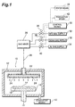
- Fig. 1 shows a chemical vapor deposition (CVD) apparatus capable of carrying out a method of forming the tungsten silicide film according to the present embodiment.
- the CVD apparatus 10 is provided with a processing chamber 12 that can be depressurized to a desired vacuum degree.
- a substrate support means e.g., pedestal 16, for supporting a substrate 14 to be processed such as a silicon wafer is provided in the processing chamber 12.
- the pedestal 16 is equipped with a heating means 18, such as a ceramic heater, for heating the silicon wafer 14.
- the heating means 18 is controlled by a control means 20, comprising a microcomputer, a memory, and so on, for controlling the entire apparatus.
- the heating means 18 controls the temperature of the pedestal 16, i.e., the stage temperature, so as to be kept at a temperature suitable for deposition. In this configuration, the heating means 18 can control the temperature of the substrate 14.
- a gas distributing plate 22 is arranged opposite to the pedestal 16.
- the gas distributing plate 22 is placed in parallel to the pedestal 16 so as to uniformly supply gas toward the substrate 14.
- the gas distributing plate 22 is a hollow plate and is provided with a plurality of gas supply ports 24 in the surface facing to the pedestal 16.
- Predetermined process gas is supplied from a gas mixing chamber 28 outside the processing chamber through a pipe 26 into the interior space of the gas distributing plate 22. Source gases and carrier gas necessary for the deposition are uniformly mixed in the gas mixing chamber 28 preliminarily.
- the apparatus is provided with process gas supply means 30, 32, 24 to form the tungsten silicide film.
- the WF 6 gas supply means 30, SiCl 2 H 2 gas (DCS gas) supply means 32, and Ar gas supply means 34 are connected via respective flow control valves 36, 38, 40 to the gas mixing chamber 28. Since the gas flow control valves 36, 38, 40 can be controlled by the control means 20, the flow rates of the respective gases are controlled in association with each other.
- the gas distributing plate 22 is made of an electroconductive material such as aluminum.
- An evacuation means 42 such as a vacuum pump is connected to the processing chamber 12. By actuating the vacuum pump, it becomes feasible to evacuate the interior of the processing chamber 12 to a desired vacuum.
- the evacuation means 42 is also controlled by the control means 20.
- the silicon semiconductor region means a polysilicon film, an amorphous silicon film, a polysilicon film made from an amorphous silicon film, or a single crystalline silicon region.
- the amorphous silicon film turns into the polysilicon film through the thermal treatment.
- the term "silicon semiconductor region" also embraces a silicon region containing germanium, i.e., SiGe.
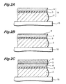
- a gate insulator film 3 is formed on the principal surface of the substrate 2 such as a silicon wafer.
- the gate insulator 3 is formed, for example, by thermally oxidizing the silicon substrate in a thermal oxidation method.
- Either of a polysilicon film and an amorphous silicon film can be deposited on the insulator 3, using a deposition apparatus such as the CVD apparatus.
- the description below concerns formation of the polysilicon film 4.
- the polysilicon film 4 can be doped with an n-type impurity such as phosphorus (P) during or after the deposition.
- the substrate 14 has the insulator 3 and polysilicon film 4 thereon.
- the substrate 14 is chemically treated with a solution containing hydrofluoric acid. This treatment removes native oxide from the surface of the polysilicon film 4.
- the substrate 14 is loaded into the CVD processing chamber 12 so as to be placed on the pedestal 16, as illustrated in Fig. 2A.
- the heating means 18 is regulated so as to maintain the stage temperature at 600°C.
- a nucleation film is formed on the polysilicon film.
- the processing chamber 12 is depressurized to a predetermined vacuum, e.g., to 1.2 Torr.
- the source gases are SiCl 2 H 2 (DSC) gas and WF 6 gas.
- the WF 6 gas supply 30, SiCl 2 H 2 (DSC) gas supply 32, and Ar gas supply 34 provide the DSC gas, WF 6 gas, and Ar carrier gas to the gas mixing chamber 28 in response to regulation of the respective valves 36, 38, 49, respectively.
- the mixed process gas is introduced via the gas distributing plate 22 into the processing chamber 12.
- the process gas is adjusted in a gas composition suitable for deposition of silicon-rich WSix film.
- the nucleation film 5 is deposited on the polysilicon film 4, as illustrated in Fig. 2B.
- the nucleation film 5 was grown to the thickness of 13 nm.
- the nucleation film 5 serves for nucleation of a subsequently grown film.
- a deposition film containing main components of tungsten and silicon is formed.
- the flow rate ratio of DSC gas/WF 6 gas is maintained at 18.4.
- the source gases of this flow rate ratio and the Ar carrier gas are supplied to the gas mixing chamber 28.
- the mixed gas is introduced through the gas distributing plate 22 into the processing chamber 12.
- the deposition film 6 is formed on the nucleation film 5, as illustrated in Fig. 2C.
- the deposition film 6 was grown to the thickness of 87 nm.
- an annealing treatment is carried out to anneal the substrate having the nucleation film 5 and the deposited film 6 thereon.
- the annealing treatment is carried out in a thermal treatment apparatus in order to change the deposited film 6 into a thermally stabler phase.
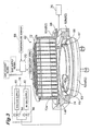
- Fig. 3 schematically shows an RTP (Rapid Thermal Processing) apparatus. This RTP apparatus is suitable for carrying out the annealing treatment for formation of the tungsten silicide film according to the present embodiment.
- the RTP apparatus 60 is provided with a processing chamber 62.
- the processing chamber 62 has a base portion 62a, a side wall portion 62b, and a lid portion 62c.
- a substrate support section 66 is provided in the processing chamber 62 so as to support a wafer (W) 64.
- the substrate support section 66 includes a cylinder frame 65 and a ring frame 65 .
- the cylinder frame 65 is mounted through a bearing on the base portion 62a.
- the ring frame 65 is arranged at the upper end of the cylinder frame 65.
- the ring frame 65 has a support step 66a supporting the edge of the wafer W at the inside edge of the frame 65.
- the wafer W is mounted so as to fit the support step 66a.
- a heating lamp array 72 is located above the lid portion 62c.
- the heating lamp array 72 includes a plurality of heating lamps 72a for heating the wafer W placed on the substrate support section 66.
- the lid portion 62c is provided with lamp windows Lw at locations of the respective heating lamps 72a. Heat from the heating lamps 72a transfers through the lamp windows Lw onto the wafer surface.
- Temperature sensors 68 for optically detecting the temperature of the wafer W are provided on a circular plate 63 of the base portion 62a. In the drawing, only one temperature sensor 68 is depicted as an example.
- the temperature sensors 68 are able to send signals concerning the temperature to a control circuit 70 including a microcomputer and memory for controlling the entire apparatus.
- Each of the heating lamps 72a is controlled according to a signal from the control circuit 70 so as to keep the temperature constant on the surface of the substrate 64. This control makes it feasible to uniformly activate a deposited film on the substrate 64.
- a gas inlet 74 and a gas outlet 88 are provided in the side wall portion 62b of the processing chamber 62.
- a gas supply means 78 is connected via flow control valves 84, 86 to the gas inlet 74.
- the gas supply means 78 includes an ammonia supply 80 and an N 2 supply 82.
- the ammonia supply 80 and N 2 supply 82 feed the process gases for the annealing to the processing chamber 62.
- a gas exhaust means 76 is connected to the gas outlet 88.
- the gas supply means 78 and the gas exhaust means 76 are controlled by the control circuit 70. In this apparatus, the controls such as the switching of the gases and the flow rate thereof are carried out in predetermined procedures.
- the substrate 64 having the deposited film 6 thereon is provided with the annealing treatment.
- the surface of the substrate 64 is chemically treated with a surface treatment solution such as a hydrofluoric-acid-based solution. This treatment removes native oxide from the surface of the substrate 64.
- the substrate 64 is loaded into the processing chamber 62 so as to be placed on the pedestal 66.
- the processing chamber 62 is depressurized to a predetermined vacuum, e.g., to 740 Torr. Only N 2 gas is first supplied as a process gas by regulating the valve 86. Then only NH 3 gas is supplied to the gas mixing chamber 78 by regulating the valve 84 of the NH 3 gas supply 80 and the valve 86 of the N 2 gas supply means 82. This process gas is introduced through a pipe 76 and via the gas inlet 74 into the processing chamber 62. This provides an ammonia atmosphere in the processing chamber 62. In the present embodiment, the flow rate of the NH 3 gas was set to 2 liters per minute.
- the heating lamps 72 are turned on to quickly increase the temperature of the substrate 64 to 1000°C.
- the temperature of the substrate 64 is maintained at 1000°C for 30 seconds.
- the heating lamps 72 are turned off to quickly decrease the temperature of the substrate 64. This completes the annealing.
- the temperature range of not less than 900°C and not more than 1100°C is also applicable to the annealing.
- a silicon nitride film is formed on the surface of the tungsten silicide film.
- This silicon nitride film is effective to protect the tungsten silicide film from chemical processing carried out in post-stages and is also effective as a barrier for preventing the dopant of phosphorus (P) and/or boron (B) in the polysilicon layer from migrating from the tungsten silicide film during the annealing.
- P phosphorus
- B boron
- the silicon nitride film can also prevent the diffusion of the dopant (impurity) in the underlying polysilicon film. Therefore, this also results in the decrease in the resistance of the underlying polysilicon film.
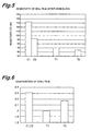
- Fig. 4A is a spectrum showing X-ray diffraction patterns measured just after the deposition in the CVD method.
- the horizontal axis represents double diffraction angles ⁇ , i.e., 2 ⁇ in units of degrees, and the vertical axis represents diffraction intensity in arbitrary units.
- the peak corresponding to (100) of the hexagonal phase becomes prominent in the deposition at stage temperatures over 550°C, e.g., at 600°C,. This peak becomes larger as the stage temperature increases. This indicates that the hexagonal phase grows during the deposition. On the other hand, this peak is not prominent in the deposition at the stage temperature of 550°C.
- Fig. 4B is a spectrum showing X-ray diffraction patterns measured after the annealing treatment of the tungsten silicide film.
- the horizontal axis represents double diffraction angles ⁇ , i.e., 2 ⁇ in units of degrees, and the vertical axis represents diffraction intensity in arbitrary units.
- the peak corresponding to (002) of the tetragonal phase becomes prominent in the deposition at stage temperatures over 550°C. This peak becomes larger as the stage temperature increases. This indicates that the tetragonal phase polycrystal is formed in the annealing. However, no specific peak appears prominent in the deposition at the stage temperature of 550°C.
- the main crystalline phase in the tungsten silicide film as deposited is preferably the hexagonal phase when the tungsten silicide film is deposited in a CVD method.
- Conditions T2 correspond to the present embodiment.
- the flow rate ratio means a flow rate ratio of DSC gas/WF 6 gas.
- RTA indicates Rapid Thermal Annealing.
- RTN represents Rapid Thermal Nitridation.
- the annealing time under the conditions C1 is about 30 minutes and the annealing time is 30 seconds under the conditions C2, T1, and T2. Under the conditions C1, the annealing treatment was conducted at the temperature of 850°C in the N 2 atmosphere, and under the condition C2 the annealing treatment was conducted at the temperature of 1000°C in the N 2 atmosphere.
- Fig. 5 shows the resistivities after the annealing. Samples used in this measurement exhibited the following resistivities:
- Fig. 6 shows compositions of deposition films before the annealing treatment.
- the Si/W ratio is over 2.3.
- the Si/W ratio is less than 2.0.
- the Si/W ratio is approximately 2.2.
- the stage temperature is preferably higher than 550°C.
- the ratios in Fig. 6 were determined based on the measurement by RBS (Rutherford Back Scattering) spectroscopy.
- Fig. 7 shows thickness differences of the tungsten silicide (WSix) film and the underlying polysilicon (DASi) film between before and after the annealing treatment for the conditions T1 and T2.
- the horizontal axis indicates each of the conditions and the vertical axis indicates change of thickness in units of nm.
- the left part indicates the Wsix film and the right part indicates the DASi film.
- the negative sign indicates decrease of thickness.
- the conditions T2 provide the tungsten silicide film with the reduced thickness variation between before and after the annealing treatment.
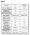
- Fig. 8 shows data under the conditions T2 according to the present embodiment, and the comparative data under the reference conditions R.
- stage temperature The deposition temperature is 600°C in the conditions T2, whereas the deposition temperature is 510°C in the reference conditions R for comparative data. From the data presented above, the inventor thought that it was preferable to carry out the formation of the tungsten silicide film at the high temperatures as disclosed in the present specification.
- the flow rate ratio means a ratio of flow rates of DSC gas/WF 6 gas. In the conditions T2, the flow rate ratio is 18.4, whereas the flow rate ratio is 43.8 in the reference conditions R for comparative data.
- the main crystal phase is the hexagonal phase in the conditions T2, whereas the amorphous phase is formed in the reference conditions R for comparative data.
- the resistivity before the annealing treatment is 825 ⁇ ⁇ cm, while the resistivity after the annealing is 68.8 ⁇ ⁇ cm.
- the annealing treatment decreases the resistivity to below about one tenth.
- the resistivity is 240 ⁇ ⁇ cm before the annealing treatment and the resistivity is 36 ⁇ ⁇ cm after the annealing treatment.
- the data demonstrates the resistivity is larger than that of the comparative data, but even the resistivity in the data is satisfactorily applicable in practice.
- the tungsten silicide film exhibits the thickness increase of about 5 nm (50 ⁇ ), whereas the underlying polysilicon film exhibits the thickness decrease of about 0 nm (0 ⁇ ).
- the tungsten silicide film demonstrates the thickness increase of about 35 nm (350 ⁇ ). Accordingly, the data in the conditions T2 of the present specification is overwhelmingly superior to the comparative data.
- the deposited film is annealed at 1000°C for 30 seconds.
- the reference conditions R for comparative data the deposited film is annealed at 900°C for 30 seconds. The experiments indicate that increase in the annealing temperature yields the WSi film having lower resistivity.
- the deposited film is particularly superior in the thickness variation in the conditions T2 according to the present embodiment. This makes it feasible to avoid the problem of delamination of the polycide film, even with further progress in scaling-down semiconductor integrated circuits.
- the resistivity of the tungsten silicide film has also been lowered to the practically applicable level.
- FIG. 9 is a cross-sectional view showing an embodiment of the method of fabricating metal-oxide-semiconductor (MOS) transistors.
- N-channel MOS device 110 and p-channel MOS device 120 will be formed on a substrate 102.
- the substrate 102 has a p-type epitaxial layer 106 on a p-type high-concentration wafer 104.
- the n-channel device 110 is formed on the p-type epitaxial layer 106.
- an n-well 108 is formed so as to include a predetermined region on the substrate.
- Device isolation film 130a, 130b, 130c are formed in order to isolate the n-channel device 110 and p-channel device 120 from each other.
- the device isolation film 130a to 130c surrounds individual device-forming regions.
- the n-channel device 110 is located between the device isolation film 130a, 130b.
- the p-channel device 110 is located between the device isolation film 130b, 130c.
- a gate insulator film 132 is formed.
- the gate insulators are formed in the respective device-forming regions in the thermal oxidation method.
- Gate electrodes 134a to 134e having the polycide structure are formed on the gate insulators 132.
- a phosphorus-doped polysilicon film is formed on the gate insulators 132 and then a tungsten silicide film is formed thereon.
- the deposition method of the embodiment as described previously can be applied to the formation of this tungsten silicide layer.
- a resist layer is formed using the photolithographic method.
- the tungsten silicide film and the polysilicon layer are etched in a dry etching method using this resist layer as a mask, thereby forming the gate electrodes 134a to 134e.
- impurities are introduced into regions 118, 128 immediately below the gate electrodes 134a, 130b in an ion implantation method.
- n-type source diffusion region 112 and n-type drain diffusion region 114 are formed in a self-aligning manner with reference to the gate electrode 134a.
- P-type source diffusion region 122 and p-type drain diffusion region 124 are formed in a self-aligning manner with reference to the gate electrode 134b.
- N-type diffusion layer 116 is a contact diffusion layer to the p-type epitaxial layer 106
- p-type diffusion layer 126 is a contact diffusion layer to the n-well 108.
- a silicon oxide film 138 such as a BPSG film is formed.
- the silicon oxide film 138 works as an interlayer dielectric film.
- the silicon oxide film 138 is formed, for example, in the thickness of 800 nm using the CVD method.
- contact holes are formed in the silicon oxide film 138 so as to reach the diffusion layers and gate electrodes on the surface of the substrate 102. These contact holes are formed, for example, by the photolithographic process and dry etching process.
- Buried plugs 140 such as tungsten plugs (W-plugs), are formed in the contact holes. Prior to the burying step of tungsten, TiW films can be formed on the bottom and side surfaces of the contact holes if necessary.
- the TiW films and W-plugs are formed, for example, in the sputtering method and in the CVD method, respectively.
- the silicon oxide film 138 and buried plugs 140 are planarized in the CMP method.
- a wiring layer 142 is formed on the planarized silicon oxide film 138.
- the wiring layer 142 can comprise, for example, three layers of TiW film, Cu film, and TiW film.
- the TiW film is made by sputtering and the Cu film is made by electroplating. Then, a predetermined wiring pattern is formed in the photolithographic method and the dry etching method.
- the wiring layer 142 has the thickness of 500 nm, for example.
- a passivation film 144 such as a plasma-nitrided film, is formed on the wiring layer 142.
- the embodiment as described above realizes the polycide gates meeting both the increasing needs for lower resistance and for smaller thickness change with progress in scaling-down for higher integration. Therefore, the scaling-down can be advanced without employing polymetal gates for the gate electrodes. Accordingly, there is no need for bearing the cost for facilities and techniques necessary for realizing the polymetal gates.
- the CVD method is adopted using the source gases including WF 6 and Si 2 H 2 Cl 2 .
- the deposited film, containing silicon and tungsten as main constitutive elements, is formed in this CVD method.
- This deposited film can mainly include the hexagonal crystal phase, or is formed at the temperature over the stage temperature of 550°C. Then, this deposited film is thermally treated in the ammonia atmosphere.
- This step ensures the composition defined by the formation of the hexagonal crystal phase, i.e., the value of x in WSi x , so that change the thickness difference of the tungsten silicide film is reduced between before and after the thermal treatment.
- This tungsten silicide film can be applied to the gate electrodes of the MIS transistors. This application reduces the occurrence of troubles, such as delamination of the gate electrode, and allows the fabrication of the MIS transistors having gate electrodes of low resistance.
- the invention provides the method of forming the tungsten silicide film exhibiting small change in the thickness of the WSi film between before and after the thermal treatment, and the method of fabricating the metal-insulator-semiconductor transistor.
Landscapes
- Engineering & Computer Science (AREA)
- Physics & Mathematics (AREA)
- Power Engineering (AREA)
- Microelectronics & Electronic Packaging (AREA)
- Computer Hardware Design (AREA)
- Manufacturing & Machinery (AREA)
- General Physics & Mathematics (AREA)
- Condensed Matter Physics & Semiconductors (AREA)
- High Energy & Nuclear Physics (AREA)
- Optics & Photonics (AREA)
- Toxicology (AREA)
- Health & Medical Sciences (AREA)
- Electromagnetism (AREA)
- Chemical & Material Sciences (AREA)
- Chemical Kinetics & Catalysis (AREA)
- Electrodes Of Semiconductors (AREA)
- Insulated Gate Type Field-Effect Transistor (AREA)
- Internal Circuitry In Semiconductor Integrated Circuit Devices (AREA)
- Chemical Vapour Deposition (AREA)
Applications Claiming Priority (3)
| Application Number | Priority Date | Filing Date | Title |
|---|---|---|---|
| JP27960999 | 1999-09-30 | ||
| JP27960999A JP2001110750A (ja) | 1999-09-30 | 1999-09-30 | タングステンシリサイド膜を形成する方法、および金属−絶縁膜−半導体型トランジスタを製造する方法 |
| PCT/JP2000/006791 WO2001024238A1 (fr) | 1999-09-30 | 2000-09-29 | Procede de formation de films de siliciure de tungstene et procede de fabrication de transistors metal-isolant-semi-conducteur |
Publications (1)
| Publication Number | Publication Date |
|---|---|
| EP1156517A1 true EP1156517A1 (en) | 2001-11-21 |
Family
ID=17613378
Family Applications (1)
| Application Number | Title | Priority Date | Filing Date |
|---|---|---|---|
| EP00962996A Withdrawn EP1156517A1 (en) | 1999-09-30 | 2000-09-29 | Method for forming tungsten silicide film and method for fabricating metal-insulator-semiconductor transistor |
Country Status (5)
| Country | Link |
|---|---|
| EP (1) | EP1156517A1 (enExample) |
| JP (1) | JP2001110750A (enExample) |
| KR (1) | KR20010080635A (enExample) |
| TW (1) | TW469517B (enExample) |
| WO (1) | WO2001024238A1 (enExample) |
Cited By (2)
| Publication number | Priority date | Publication date | Assignee | Title |
|---|---|---|---|---|
| US6827796B2 (en) * | 2000-11-02 | 2004-12-07 | Composite Tool Company, Inc. | High strength alloys and methods for making same |
| US10763373B2 (en) | 2015-07-14 | 2020-09-01 | Semiconductor Energy Laboratory Co., Ltd. | Semiconductor device |
Families Citing this family (7)
| Publication number | Priority date | Publication date | Assignee | Title |
|---|---|---|---|---|
| KR100669141B1 (ko) * | 2005-01-17 | 2007-01-15 | 삼성전자주식회사 | 오믹막 및 이의 형성 방법, 오믹막을 포함하는 반도체장치 및 이의 제조 방법 |
| KR100680969B1 (ko) * | 2005-08-18 | 2007-02-09 | 주식회사 하이닉스반도체 | 텅스텐실리사이드 박막 형성방법 |
| TWI395254B (zh) * | 2006-01-25 | 2013-05-01 | Air Water Inc | Film forming device |
| TWI341012B (en) | 2007-09-03 | 2011-04-21 | Macronix Int Co Ltd | Methods of forming nitride read only memory and word lines thereof |
| JP2011258811A (ja) * | 2010-06-10 | 2011-12-22 | Ulvac Japan Ltd | 半導体装置の製造方法 |
| KR101035738B1 (ko) * | 2011-02-24 | 2011-05-20 | 주식회사 문라이트 | 보행자 및 자전거 도로용 조명기구 |
| KR102349420B1 (ko) | 2015-02-17 | 2022-01-10 | 삼성전자 주식회사 | 메탈 실리사이드층 형성방법 및 그 방법을 이용한 반도체 소자의 제조방법 |
Family Cites Families (5)
| Publication number | Priority date | Publication date | Assignee | Title |
|---|---|---|---|---|
| JP2657306B2 (ja) * | 1988-07-29 | 1997-09-24 | 東京エレクトロン株式会社 | 金属シリサイド膜の形成方法 |
| JPH06216066A (ja) * | 1993-01-14 | 1994-08-05 | Fujitsu Ltd | 半導体装置の製造方法 |
| EP0704551B1 (en) * | 1994-09-27 | 2000-09-06 | Applied Materials, Inc. | Method of processing a substrate in a vacuum processing chamber |
| EP0746027A3 (en) * | 1995-05-03 | 1998-04-01 | Applied Materials, Inc. | Polysilicon/tungsten silicide multilayer composite formed on an integrated circuit structure, and improved method of making same |
| JPH0917998A (ja) * | 1995-06-28 | 1997-01-17 | Sony Corp | Mosトランジスタの製造方法 |
-
1999
- 1999-09-30 JP JP27960999A patent/JP2001110750A/ja not_active Withdrawn
-
2000
- 2000-09-29 KR KR1020017006766A patent/KR20010080635A/ko not_active Ceased
- 2000-09-29 TW TW089120316A patent/TW469517B/zh not_active IP Right Cessation
- 2000-09-29 WO PCT/JP2000/006791 patent/WO2001024238A1/ja not_active Ceased
- 2000-09-29 EP EP00962996A patent/EP1156517A1/en not_active Withdrawn
Non-Patent Citations (1)
| Title |
|---|
| See references of WO0124238A1 * |
Cited By (5)
| Publication number | Priority date | Publication date | Assignee | Title |
|---|---|---|---|---|
| US6827796B2 (en) * | 2000-11-02 | 2004-12-07 | Composite Tool Company, Inc. | High strength alloys and methods for making same |
| US10763373B2 (en) | 2015-07-14 | 2020-09-01 | Semiconductor Energy Laboratory Co., Ltd. | Semiconductor device |
| US11393930B2 (en) | 2015-07-14 | 2022-07-19 | Semiconductor Energy Laboratory Co., Ltd. | Semiconductor device |
| US12046683B2 (en) | 2015-07-14 | 2024-07-23 | Semiconductor Energy Laboratory Co., Ltd. | Semiconductor device |
| US12389636B2 (en) | 2015-07-14 | 2025-08-12 | Semiconductor Energy Laboratory Co., Ltd. | Semiconductor device |
Also Published As
| Publication number | Publication date |
|---|---|
| WO2001024238A1 (fr) | 2001-04-05 |
| TW469517B (en) | 2001-12-21 |
| JP2001110750A (ja) | 2001-04-20 |
| KR20010080635A (ko) | 2001-08-22 |
Similar Documents
| Publication | Publication Date | Title |
|---|---|---|
| US8476714B2 (en) | Semiconductor device | |
| US20080246101A1 (en) | Method of poly-silicon grain structure formation | |
| US8110457B2 (en) | Method of manufacturing semiconductor device | |
| US6991999B2 (en) | Bi-layer silicon film and method of fabrication | |
| US20040178437A1 (en) | Methods for forming wordlines, transistor gates, and conductive interconnects, and wordline, transistor gate, and conductive interconnect structures | |
| WO2003060184A2 (en) | Method and apparatus for forming silicon containing films | |
| US20090065816A1 (en) | Modulating the stress of poly-crystaline silicon films and surrounding layers through the use of dopants and multi-layer silicon films with controlled crystal structure | |
| US7193270B2 (en) | Semiconductor device with a vertical transistor | |
| US7875939B2 (en) | Semiconductor device including an ohmic layer | |
| EP1156517A1 (en) | Method for forming tungsten silicide film and method for fabricating metal-insulator-semiconductor transistor | |
| US6632721B1 (en) | Method of manufacturing semiconductor devices having capacitors with electrode including hemispherical grains | |
| US6930335B2 (en) | Field effect transistor with metal oxide gate insulator and sidewall insulating film | |
| JP4441109B2 (ja) | 半導体装置の製造方法 | |
| JP3156590B2 (ja) | 半導体装置及びその製造方法 | |
| US20050085071A1 (en) | Methods of forming conductive metal silicides by reaction of metal with silicon | |
| US6599820B1 (en) | Method of producing a semiconductor device | |
| GB2306781A (en) | Method for forming metal wiring of semiconductor devices | |
| US8115263B2 (en) | Laminated silicon gate electrode | |
| US7375015B2 (en) | Manufacturing method which prevents abnormal gate oxidation | |
| US20030045081A1 (en) | MOSFET having a stacked silicon structure and method | |
| JPH04336466A (ja) | 半導体装置の製造方法 | |
| JP3092594B2 (ja) | 高融点金属ポリサイド構造を有する半導体装置及びその製造方法 | |
| KR100472855B1 (ko) | 반도체소자의다결정실리콘박막제조방법 | |
| KR100364524B1 (ko) | 텅스텐 실리사이드 단층 게이트 구조를 갖는 모스 트랜지스터의 제조방법 | |
| KR20010043753A (ko) | 박막의 열처리방법 및 박막의 형성방법 |
Legal Events
| Date | Code | Title | Description |
|---|---|---|---|
| PUAI | Public reference made under article 153(3) epc to a published international application that has entered the european phase |
Free format text: ORIGINAL CODE: 0009012 |
|
| 17P | Request for examination filed |
Effective date: 20010612 |
|
| AK | Designated contracting states |
Kind code of ref document: A1 Designated state(s): AT BE CH CY DE DK ES FI FR GB GR IE IT LI LU MC NL PT SE |
|
| STAA | Information on the status of an ep patent application or granted ep patent |
Free format text: STATUS: THE APPLICATION HAS BEEN WITHDRAWN |
|
| 18W | Application withdrawn |
Effective date: 20041215 |