US8110457B2 - Method of manufacturing semiconductor device - Google Patents
Method of manufacturing semiconductor device Download PDFInfo
- Publication number
- US8110457B2 US8110457B2 US12/563,144 US56314409A US8110457B2 US 8110457 B2 US8110457 B2 US 8110457B2 US 56314409 A US56314409 A US 56314409A US 8110457 B2 US8110457 B2 US 8110457B2
- Authority
- US
- United States
- Prior art keywords
- heat treatment
- alloy film
- silicide layer
- metal silicide
- thickness
- Prior art date
- Legal status (The legal status is an assumption and is not a legal conclusion. Google has not performed a legal analysis and makes no representation as to the accuracy of the status listed.)
- Active, expires
Links
- 239000004065 semiconductor Substances 0.000 title claims abstract description 377
- 238000004519 manufacturing process Methods 0.000 title claims description 67
- 229910045601 alloy Inorganic materials 0.000 claims abstract description 452
- 239000000956 alloy Substances 0.000 claims abstract description 452
- 238000010438 heat treatment Methods 0.000 claims abstract description 427
- 229910052751 metal Inorganic materials 0.000 claims abstract description 399
- 239000002184 metal Substances 0.000 claims abstract description 378
- 229910021332 silicide Inorganic materials 0.000 claims abstract description 293
- FVBUAEGBCNSCDD-UHFFFAOYSA-N silicide(4-) Chemical compound [Si-4] FVBUAEGBCNSCDD-UHFFFAOYSA-N 0.000 claims abstract description 293
- 238000000034 method Methods 0.000 claims abstract description 99
- 239000000758 substrate Substances 0.000 claims abstract description 67
- 238000009792 diffusion process Methods 0.000 claims abstract description 44
- PXHVJJICTQNCMI-UHFFFAOYSA-N Nickel Chemical compound [Ni] PXHVJJICTQNCMI-UHFFFAOYSA-N 0.000 claims description 186
- 229910052759 nickel Inorganic materials 0.000 claims description 27
- 229910052697 platinum Inorganic materials 0.000 claims description 19
- 238000005530 etching Methods 0.000 claims description 11
- 238000001312 dry etching Methods 0.000 claims description 4
- 229910052691 Erbium Inorganic materials 0.000 claims description 2
- 229910052769 Ytterbium Inorganic materials 0.000 claims description 2
- 229910052763 palladium Inorganic materials 0.000 claims description 2
- 229910052720 vanadium Inorganic materials 0.000 claims description 2
- 230000008569 process Effects 0.000 abstract description 60
- 239000010410 layer Substances 0.000 description 319
- BASFCYQUMIYNBI-UHFFFAOYSA-N platinum Substances [Pt] BASFCYQUMIYNBI-UHFFFAOYSA-N 0.000 description 209
- XUIMIQQOPSSXEZ-UHFFFAOYSA-N Silicon Chemical compound [Si] XUIMIQQOPSSXEZ-UHFFFAOYSA-N 0.000 description 136
- 229910052710 silicon Inorganic materials 0.000 description 136
- 239000010703 silicon Substances 0.000 description 136
- 235000012431 wafers Nutrition 0.000 description 114
- 229910015509 Ni1-yMy Inorganic materials 0.000 description 70
- 229910015258 Ni1−yMy Inorganic materials 0.000 description 70
- 239000007789 gas Substances 0.000 description 61
- 238000006243 chemical reaction Methods 0.000 description 60
- 238000000151 deposition Methods 0.000 description 56
- 230000008021 deposition Effects 0.000 description 52
- 230000015572 biosynthetic process Effects 0.000 description 51
- 230000004888 barrier function Effects 0.000 description 43
- 230000001965 increasing effect Effects 0.000 description 32
- 239000012535 impurity Substances 0.000 description 29
- 150000002500 ions Chemical class 0.000 description 25
- 238000010586 diagram Methods 0.000 description 21
- 229910015500 Ni1-xMx Inorganic materials 0.000 description 20
- 229910001260 Pt alloy Inorganic materials 0.000 description 19
- 230000003247 decreasing effect Effects 0.000 description 18
- 238000005108 dry cleaning Methods 0.000 description 18
- 230000007423 decrease Effects 0.000 description 17
- 229910021334 nickel silicide Inorganic materials 0.000 description 17
- RUFLMLWJRZAWLJ-UHFFFAOYSA-N nickel silicide Chemical compound [Ni]=[Si]=[Ni] RUFLMLWJRZAWLJ-UHFFFAOYSA-N 0.000 description 17
- IJGRMHOSHXDMSA-UHFFFAOYSA-N Atomic nitrogen Chemical compound N#N IJGRMHOSHXDMSA-UHFFFAOYSA-N 0.000 description 16
- 230000000694 effects Effects 0.000 description 15
- 239000000463 material Substances 0.000 description 15
- 229920002120 photoresistant polymer Polymers 0.000 description 13
- 238000004544 sputter deposition Methods 0.000 description 12
- VYPSYNLAJGMNEJ-UHFFFAOYSA-N Silicium dioxide Chemical compound O=[Si]=O VYPSYNLAJGMNEJ-UHFFFAOYSA-N 0.000 description 11
- 230000002159 abnormal effect Effects 0.000 description 11
- 239000000203 mixture Substances 0.000 description 11
- 238000007254 oxidation reaction Methods 0.000 description 11
- 230000003647 oxidation Effects 0.000 description 10
- 239000002245 particle Substances 0.000 description 10
- 230000005669 field effect Effects 0.000 description 9
- 239000011261 inert gas Substances 0.000 description 9
- 238000005468 ion implantation Methods 0.000 description 9
- 229910021420 polycrystalline silicon Inorganic materials 0.000 description 9
- 229920005591 polysilicon Polymers 0.000 description 9
- 229910052814 silicon oxide Inorganic materials 0.000 description 9
- 239000013078 crystal Substances 0.000 description 8
- ZOXJGFHDIHLPTG-UHFFFAOYSA-N Boron Chemical compound [B] ZOXJGFHDIHLPTG-UHFFFAOYSA-N 0.000 description 7
- OKTJSMMVPCPJKN-UHFFFAOYSA-N Carbon Chemical compound [C] OKTJSMMVPCPJKN-UHFFFAOYSA-N 0.000 description 7
- 229910052785 arsenic Inorganic materials 0.000 description 7
- RQNWIZPPADIBDY-UHFFFAOYSA-N arsenic atom Chemical compound [As] RQNWIZPPADIBDY-UHFFFAOYSA-N 0.000 description 7
- 230000008901 benefit Effects 0.000 description 7
- 229910052796 boron Inorganic materials 0.000 description 7
- 229910052799 carbon Inorganic materials 0.000 description 7
- 229910052732 germanium Inorganic materials 0.000 description 7
- GNPVGFCGXDBREM-UHFFFAOYSA-N germanium atom Chemical compound [Ge] GNPVGFCGXDBREM-UHFFFAOYSA-N 0.000 description 7
- 229910052754 neon Inorganic materials 0.000 description 7
- 238000005268 plasma chemical vapour deposition Methods 0.000 description 7
- 229910019975 (NH4)2SiF6 Inorganic materials 0.000 description 6
- OAICVXFJPJFONN-UHFFFAOYSA-N Phosphorus Chemical compound [P] OAICVXFJPJFONN-UHFFFAOYSA-N 0.000 description 6
- 229910052581 Si3N4 Inorganic materials 0.000 description 6
- NRTOMJZYCJJWKI-UHFFFAOYSA-N Titanium nitride Chemical compound [Ti]#N NRTOMJZYCJJWKI-UHFFFAOYSA-N 0.000 description 6
- 229910017052 cobalt Inorganic materials 0.000 description 6
- 239000010941 cobalt Substances 0.000 description 6
- GUTLYIVDDKVIGB-UHFFFAOYSA-N cobalt atom Chemical compound [Co] GUTLYIVDDKVIGB-UHFFFAOYSA-N 0.000 description 6
- 229910001873 dinitrogen Inorganic materials 0.000 description 6
- 229910052734 helium Inorganic materials 0.000 description 6
- 239000012212 insulator Substances 0.000 description 6
- 238000002955 isolation Methods 0.000 description 6
- GKAOGPIIYCISHV-UHFFFAOYSA-N neon atom Chemical compound [Ne] GKAOGPIIYCISHV-UHFFFAOYSA-N 0.000 description 6
- 229910052698 phosphorus Inorganic materials 0.000 description 6
- 239000011574 phosphorus Substances 0.000 description 6
- HQVNEWCFYHHQES-UHFFFAOYSA-N silicon nitride Chemical compound N12[Si]34N5[Si]62N3[Si]51N64 HQVNEWCFYHHQES-UHFFFAOYSA-N 0.000 description 6
- 239000010936 titanium Substances 0.000 description 6
- RYGMFSIKBFXOCR-UHFFFAOYSA-N Copper Chemical compound [Cu] RYGMFSIKBFXOCR-UHFFFAOYSA-N 0.000 description 5
- 229910000676 Si alloy Inorganic materials 0.000 description 5
- 230000001133 acceleration Effects 0.000 description 5
- 238000004140 cleaning Methods 0.000 description 5
- 238000001816 cooling Methods 0.000 description 5
- 229910052802 copper Inorganic materials 0.000 description 5
- 239000010949 copper Substances 0.000 description 5
- 239000001307 helium Substances 0.000 description 5
- SWQJXJOGLNCZEY-UHFFFAOYSA-N helium atom Chemical compound [He] SWQJXJOGLNCZEY-UHFFFAOYSA-N 0.000 description 5
- 238000003475 lamination Methods 0.000 description 5
- 230000007246 mechanism Effects 0.000 description 5
- 229910021421 monocrystalline silicon Inorganic materials 0.000 description 5
- XKRFYHLGVUSROY-UHFFFAOYSA-N Argon Chemical compound [Ar] XKRFYHLGVUSROY-UHFFFAOYSA-N 0.000 description 4
- QAOWNCQODCNURD-UHFFFAOYSA-N Sulfuric acid Chemical compound OS(O)(=O)=O QAOWNCQODCNURD-UHFFFAOYSA-N 0.000 description 4
- RTAQQCXQSZGOHL-UHFFFAOYSA-N Titanium Chemical compound [Ti] RTAQQCXQSZGOHL-UHFFFAOYSA-N 0.000 description 4
- 238000005054 agglomeration Methods 0.000 description 4
- 230000002776 aggregation Effects 0.000 description 4
- 229910052757 nitrogen Inorganic materials 0.000 description 4
- 230000001629 suppression Effects 0.000 description 4
- 238000007669 thermal treatment Methods 0.000 description 4
- 229910052719 titanium Inorganic materials 0.000 description 4
- BOTDANWDWHJENH-UHFFFAOYSA-N Tetraethyl orthosilicate Chemical compound CCO[Si](OCC)(OCC)OCC BOTDANWDWHJENH-UHFFFAOYSA-N 0.000 description 3
- 230000002411 adverse Effects 0.000 description 3
- QVGXLLKOCUKJST-UHFFFAOYSA-N atomic oxygen Chemical compound [O] QVGXLLKOCUKJST-UHFFFAOYSA-N 0.000 description 3
- 239000001301 oxygen Substances 0.000 description 3
- 229910052760 oxygen Inorganic materials 0.000 description 3
- KDLHZDBZIXYQEI-UHFFFAOYSA-N palladium Substances [Pd] KDLHZDBZIXYQEI-UHFFFAOYSA-N 0.000 description 3
- 238000000206 photolithography Methods 0.000 description 3
- 238000001020 plasma etching Methods 0.000 description 3
- 238000007747 plating Methods 0.000 description 3
- 230000002265 prevention Effects 0.000 description 3
- 125000006850 spacer group Chemical group 0.000 description 3
- WFKWXMTUELFFGS-UHFFFAOYSA-N tungsten Chemical compound [W] WFKWXMTUELFFGS-UHFFFAOYSA-N 0.000 description 3
- KRHYYFGTRYWZRS-UHFFFAOYSA-N Fluorane Chemical compound F KRHYYFGTRYWZRS-UHFFFAOYSA-N 0.000 description 2
- 229910000990 Ni alloy Inorganic materials 0.000 description 2
- 229910012990 NiSi2 Inorganic materials 0.000 description 2
- 229910052786 argon Inorganic materials 0.000 description 2
- 238000005229 chemical vapour deposition Methods 0.000 description 2
- 239000004020 conductor Substances 0.000 description 2
- 238000005137 deposition process Methods 0.000 description 2
- 239000000428 dust Substances 0.000 description 2
- -1 for example Chemical compound 0.000 description 2
- 230000012447 hatching Effects 0.000 description 2
- 239000001257 hydrogen Substances 0.000 description 2
- 229910052739 hydrogen Inorganic materials 0.000 description 2
- 230000006872 improvement Effects 0.000 description 2
- 238000002354 inductively-coupled plasma atomic emission spectroscopy Methods 0.000 description 2
- 230000005764 inhibitory process Effects 0.000 description 2
- 239000011229 interlayer Substances 0.000 description 2
- 239000002923 metal particle Substances 0.000 description 2
- 150000004767 nitrides Chemical class 0.000 description 2
- 230000035515 penetration Effects 0.000 description 2
- 230000000087 stabilizing effect Effects 0.000 description 2
- 239000000126 substance Substances 0.000 description 2
- 229910052721 tungsten Inorganic materials 0.000 description 2
- 239000010937 tungsten Substances 0.000 description 2
- 230000007306 turnover Effects 0.000 description 2
- PXGOKWXKJXAPGV-UHFFFAOYSA-N Fluorine Chemical compound FF PXGOKWXKJXAPGV-UHFFFAOYSA-N 0.000 description 1
- YCKRFDGAMUMZLT-UHFFFAOYSA-N Fluorine atom Chemical compound [F] YCKRFDGAMUMZLT-UHFFFAOYSA-N 0.000 description 1
- UFHFLCQGNIYNRP-UHFFFAOYSA-N Hydrogen Chemical compound [H][H] UFHFLCQGNIYNRP-UHFFFAOYSA-N 0.000 description 1
- MHAJPDPJQMAIIY-UHFFFAOYSA-N Hydrogen peroxide Chemical compound OO MHAJPDPJQMAIIY-UHFFFAOYSA-N 0.000 description 1
- 229910018062 Ni-M Inorganic materials 0.000 description 1
- 230000003213 activating effect Effects 0.000 description 1
- 230000004913 activation Effects 0.000 description 1
- 229910002065 alloy metal Inorganic materials 0.000 description 1
- 229910021417 amorphous silicon Inorganic materials 0.000 description 1
- 238000000137 annealing Methods 0.000 description 1
- 239000003963 antioxidant agent Substances 0.000 description 1
- 230000003078 antioxidant effect Effects 0.000 description 1
- 238000004380 ashing Methods 0.000 description 1
- 229910001423 beryllium ion Inorganic materials 0.000 description 1
- 238000004364 calculation method Methods 0.000 description 1
- 230000008859 change Effects 0.000 description 1
- 229910052681 coesite Inorganic materials 0.000 description 1
- 230000000295 complement effect Effects 0.000 description 1
- 229910052906 cristobalite Inorganic materials 0.000 description 1
- 230000007547 defect Effects 0.000 description 1
- 230000009977 dual effect Effects 0.000 description 1
- 238000009713 electroplating Methods 0.000 description 1
- 230000003028 elevating effect Effects 0.000 description 1
- UYAHIZSMUZPPFV-UHFFFAOYSA-N erbium Chemical compound [Er] UYAHIZSMUZPPFV-UHFFFAOYSA-N 0.000 description 1
- 230000005284 excitation Effects 0.000 description 1
- 239000011737 fluorine Substances 0.000 description 1
- 229910052731 fluorine Inorganic materials 0.000 description 1
- XLYOFNOQVPJJNP-ZSJDYOACSA-N heavy water Substances [2H]O[2H] XLYOFNOQVPJJNP-ZSJDYOACSA-N 0.000 description 1
- BHEPBYXIRTUNPN-UHFFFAOYSA-N hydridophosphorus(.) (triplet) Chemical compound [PH] BHEPBYXIRTUNPN-UHFFFAOYSA-N 0.000 description 1
- 150000002431 hydrogen Chemical class 0.000 description 1
- 230000010354 integration Effects 0.000 description 1
- 230000004048 modification Effects 0.000 description 1
- 238000012986 modification Methods 0.000 description 1
- 238000003032 molecular docking Methods 0.000 description 1
- PCLURTMBFDTLSK-UHFFFAOYSA-N nickel platinum Chemical compound [Ni].[Pt] PCLURTMBFDTLSK-UHFFFAOYSA-N 0.000 description 1
- 229910021340 platinum monosilicide Inorganic materials 0.000 description 1
- 238000005498 polishing Methods 0.000 description 1
- 230000001681 protective effect Effects 0.000 description 1
- 239000012495 reaction gas Substances 0.000 description 1
- 239000000377 silicon dioxide Substances 0.000 description 1
- 239000002356 single layer Substances 0.000 description 1
- 229910052682 stishovite Inorganic materials 0.000 description 1
- 230000000153 supplemental effect Effects 0.000 description 1
- 229910052715 tantalum Inorganic materials 0.000 description 1
- GUVRBAGPIYLISA-UHFFFAOYSA-N tantalum atom Chemical compound [Ta] GUVRBAGPIYLISA-UHFFFAOYSA-N 0.000 description 1
- MZLGASXMSKOWSE-UHFFFAOYSA-N tantalum nitride Chemical compound [Ta]#N MZLGASXMSKOWSE-UHFFFAOYSA-N 0.000 description 1
- 229910052905 tridymite Inorganic materials 0.000 description 1
- GPPXJZIENCGNKB-UHFFFAOYSA-N vanadium Chemical compound [V]#[V] GPPXJZIENCGNKB-UHFFFAOYSA-N 0.000 description 1
- 238000001039 wet etching Methods 0.000 description 1
- NAWDYIZEMPQZHO-UHFFFAOYSA-N ytterbium Chemical compound [Yb] NAWDYIZEMPQZHO-UHFFFAOYSA-N 0.000 description 1
Images


Classifications
-
- H—ELECTRICITY
- H01—ELECTRIC ELEMENTS
- H01L—SEMICONDUCTOR DEVICES NOT COVERED BY CLASS H10
- H01L21/00—Processes or apparatus adapted for the manufacture or treatment of semiconductor or solid state devices or of parts thereof
- H01L21/67—Apparatus specially adapted for handling semiconductor or electric solid state devices during manufacture or treatment thereof; Apparatus specially adapted for handling wafers during manufacture or treatment of semiconductor or electric solid state devices or components ; Apparatus not specifically provided for elsewhere
- H01L21/683—Apparatus specially adapted for handling semiconductor or electric solid state devices during manufacture or treatment thereof; Apparatus specially adapted for handling wafers during manufacture or treatment of semiconductor or electric solid state devices or components ; Apparatus not specifically provided for elsewhere for supporting or gripping
- H01L21/687—Apparatus specially adapted for handling semiconductor or electric solid state devices during manufacture or treatment thereof; Apparatus specially adapted for handling wafers during manufacture or treatment of semiconductor or electric solid state devices or components ; Apparatus not specifically provided for elsewhere for supporting or gripping using mechanical means, e.g. chucks, clamps or pinches
- H01L21/68714—Apparatus specially adapted for handling semiconductor or electric solid state devices during manufacture or treatment thereof; Apparatus specially adapted for handling wafers during manufacture or treatment of semiconductor or electric solid state devices or components ; Apparatus not specifically provided for elsewhere for supporting or gripping using mechanical means, e.g. chucks, clamps or pinches the wafers being placed on a susceptor, stage or support
- H01L21/68735—Apparatus specially adapted for handling semiconductor or electric solid state devices during manufacture or treatment thereof; Apparatus specially adapted for handling wafers during manufacture or treatment of semiconductor or electric solid state devices or components ; Apparatus not specifically provided for elsewhere for supporting or gripping using mechanical means, e.g. chucks, clamps or pinches the wafers being placed on a susceptor, stage or support characterised by edge profile or support profile
-
- H—ELECTRICITY
- H01—ELECTRIC ELEMENTS
- H01L—SEMICONDUCTOR DEVICES NOT COVERED BY CLASS H10
- H01L21/00—Processes or apparatus adapted for the manufacture or treatment of semiconductor or solid state devices or of parts thereof
- H01L21/02—Manufacture or treatment of semiconductor devices or of parts thereof
- H01L21/04—Manufacture or treatment of semiconductor devices or of parts thereof the devices having at least one potential-jump barrier or surface barrier, e.g. PN junction, depletion layer or carrier concentration layer
- H01L21/18—Manufacture or treatment of semiconductor devices or of parts thereof the devices having at least one potential-jump barrier or surface barrier, e.g. PN junction, depletion layer or carrier concentration layer the devices having semiconductor bodies comprising elements of Group IV of the Periodic System or AIIIBV compounds with or without impurities, e.g. doping materials
- H01L21/28—Manufacture of electrodes on semiconductor bodies using processes or apparatus not provided for in groups H01L21/20 - H01L21/268
- H01L21/28008—Making conductor-insulator-semiconductor electrodes
- H01L21/28017—Making conductor-insulator-semiconductor electrodes the insulator being formed after the semiconductor body, the semiconductor being silicon
- H01L21/28026—Making conductor-insulator-semiconductor electrodes the insulator being formed after the semiconductor body, the semiconductor being silicon characterised by the conductor
- H01L21/28035—Making conductor-insulator-semiconductor electrodes the insulator being formed after the semiconductor body, the semiconductor being silicon characterised by the conductor the final conductor layer next to the insulator being silicon, e.g. polysilicon, with or without impurities
- H01L21/28044—Making conductor-insulator-semiconductor electrodes the insulator being formed after the semiconductor body, the semiconductor being silicon characterised by the conductor the final conductor layer next to the insulator being silicon, e.g. polysilicon, with or without impurities the conductor comprising at least another non-silicon conductive layer
- H01L21/28052—Making conductor-insulator-semiconductor electrodes the insulator being formed after the semiconductor body, the semiconductor being silicon characterised by the conductor the final conductor layer next to the insulator being silicon, e.g. polysilicon, with or without impurities the conductor comprising at least another non-silicon conductive layer the conductor comprising a silicide layer formed by the silicidation reaction of silicon with a metal layer
-
- H—ELECTRICITY
- H01—ELECTRIC ELEMENTS
- H01L—SEMICONDUCTOR DEVICES NOT COVERED BY CLASS H10
- H01L21/00—Processes or apparatus adapted for the manufacture or treatment of semiconductor or solid state devices or of parts thereof
- H01L21/02—Manufacture or treatment of semiconductor devices or of parts thereof
- H01L21/04—Manufacture or treatment of semiconductor devices or of parts thereof the devices having at least one potential-jump barrier or surface barrier, e.g. PN junction, depletion layer or carrier concentration layer
- H01L21/18—Manufacture or treatment of semiconductor devices or of parts thereof the devices having at least one potential-jump barrier or surface barrier, e.g. PN junction, depletion layer or carrier concentration layer the devices having semiconductor bodies comprising elements of Group IV of the Periodic System or AIIIBV compounds with or without impurities, e.g. doping materials
- H01L21/28—Manufacture of electrodes on semiconductor bodies using processes or apparatus not provided for in groups H01L21/20 - H01L21/268
- H01L21/283—Deposition of conductive or insulating materials for electrodes conducting electric current
- H01L21/285—Deposition of conductive or insulating materials for electrodes conducting electric current from a gas or vapour, e.g. condensation
- H01L21/28506—Deposition of conductive or insulating materials for electrodes conducting electric current from a gas or vapour, e.g. condensation of conductive layers
- H01L21/28512—Deposition of conductive or insulating materials for electrodes conducting electric current from a gas or vapour, e.g. condensation of conductive layers on semiconductor bodies comprising elements of Group IV of the Periodic System
- H01L21/28518—Deposition of conductive or insulating materials for electrodes conducting electric current from a gas or vapour, e.g. condensation of conductive layers on semiconductor bodies comprising elements of Group IV of the Periodic System the conductive layers comprising silicides
-
- H—ELECTRICITY
- H01—ELECTRIC ELEMENTS
- H01L—SEMICONDUCTOR DEVICES NOT COVERED BY CLASS H10
- H01L21/00—Processes or apparatus adapted for the manufacture or treatment of semiconductor or solid state devices or of parts thereof
- H01L21/67—Apparatus specially adapted for handling semiconductor or electric solid state devices during manufacture or treatment thereof; Apparatus specially adapted for handling wafers during manufacture or treatment of semiconductor or electric solid state devices or components ; Apparatus not specifically provided for elsewhere
- H01L21/67005—Apparatus not specifically provided for elsewhere
- H01L21/67011—Apparatus for manufacture or treatment
- H01L21/67098—Apparatus for thermal treatment
- H01L21/67109—Apparatus for thermal treatment mainly by convection
-
- H—ELECTRICITY
- H01—ELECTRIC ELEMENTS
- H01L—SEMICONDUCTOR DEVICES NOT COVERED BY CLASS H10
- H01L21/00—Processes or apparatus adapted for the manufacture or treatment of semiconductor or solid state devices or of parts thereof
- H01L21/67—Apparatus specially adapted for handling semiconductor or electric solid state devices during manufacture or treatment thereof; Apparatus specially adapted for handling wafers during manufacture or treatment of semiconductor or electric solid state devices or components ; Apparatus not specifically provided for elsewhere
- H01L21/67005—Apparatus not specifically provided for elsewhere
- H01L21/67011—Apparatus for manufacture or treatment
- H01L21/67155—Apparatus for manufacturing or treating in a plurality of work-stations
- H01L21/67184—Apparatus for manufacturing or treating in a plurality of work-stations characterized by the presence of more than one transfer chamber
-
- H—ELECTRICITY
- H01—ELECTRIC ELEMENTS
- H01L—SEMICONDUCTOR DEVICES NOT COVERED BY CLASS H10
- H01L21/00—Processes or apparatus adapted for the manufacture or treatment of semiconductor or solid state devices or of parts thereof
- H01L21/67—Apparatus specially adapted for handling semiconductor or electric solid state devices during manufacture or treatment thereof; Apparatus specially adapted for handling wafers during manufacture or treatment of semiconductor or electric solid state devices or components ; Apparatus not specifically provided for elsewhere
- H01L21/67005—Apparatus not specifically provided for elsewhere
- H01L21/67011—Apparatus for manufacture or treatment
- H01L21/67155—Apparatus for manufacturing or treating in a plurality of work-stations
- H01L21/6719—Apparatus for manufacturing or treating in a plurality of work-stations characterized by the construction of the processing chambers, e.g. modular processing chambers
-
- H—ELECTRICITY
- H01—ELECTRIC ELEMENTS
- H01L—SEMICONDUCTOR DEVICES NOT COVERED BY CLASS H10
- H01L29/00—Semiconductor devices adapted for rectifying, amplifying, oscillating or switching, or capacitors or resistors with at least one potential-jump barrier or surface barrier, e.g. PN junction depletion layer or carrier concentration layer; Details of semiconductor bodies or of electrodes thereof ; Multistep manufacturing processes therefor
- H01L29/66—Types of semiconductor device ; Multistep manufacturing processes therefor
- H01L29/66007—Multistep manufacturing processes
- H01L29/66075—Multistep manufacturing processes of devices having semiconductor bodies comprising group 14 or group 13/15 materials
- H01L29/66227—Multistep manufacturing processes of devices having semiconductor bodies comprising group 14 or group 13/15 materials the devices being controllable only by the electric current supplied or the electric potential applied, to an electrode which does not carry the current to be rectified, amplified or switched, e.g. three-terminal devices
- H01L29/66409—Unipolar field-effect transistors
- H01L29/66477—Unipolar field-effect transistors with an insulated gate, i.e. MISFET
- H01L29/665—Unipolar field-effect transistors with an insulated gate, i.e. MISFET using self aligned silicidation, i.e. salicide
-
- H—ELECTRICITY
- H01—ELECTRIC ELEMENTS
- H01L—SEMICONDUCTOR DEVICES NOT COVERED BY CLASS H10
- H01L29/00—Semiconductor devices adapted for rectifying, amplifying, oscillating or switching, or capacitors or resistors with at least one potential-jump barrier or surface barrier, e.g. PN junction depletion layer or carrier concentration layer; Details of semiconductor bodies or of electrodes thereof ; Multistep manufacturing processes therefor
- H01L29/66—Types of semiconductor device ; Multistep manufacturing processes therefor
- H01L29/66007—Multistep manufacturing processes
- H01L29/66075—Multistep manufacturing processes of devices having semiconductor bodies comprising group 14 or group 13/15 materials
- H01L29/66227—Multistep manufacturing processes of devices having semiconductor bodies comprising group 14 or group 13/15 materials the devices being controllable only by the electric current supplied or the electric potential applied, to an electrode which does not carry the current to be rectified, amplified or switched, e.g. three-terminal devices
- H01L29/66409—Unipolar field-effect transistors
- H01L29/66477—Unipolar field-effect transistors with an insulated gate, i.e. MISFET
- H01L29/6656—Unipolar field-effect transistors with an insulated gate, i.e. MISFET using multiple spacer layers, e.g. multiple sidewall spacers
Definitions
- the present invention relates to a method of manufacturing a semiconductor device, and more particularly, to a technique effectively applied to the manufacture of a semiconductor element with a metal silicide layer.
- MISFETs metal insulator semiconductor field effect transistors
- a salicide (self-aligned silicide) technique which is designed to decrease the resistance of a gate or source/drain by forming a low-resistance metal silicide layer, for example, a nickel silicide layer or a cobalt silicide layer, by a self-alignment process on the surface of a conductive film forming the gate and on the surface of a semiconductor region forming the source/drain.
- Patent Document 1 discloses a technique for forming a nickel platinum monosilicide layer.
- Patent Document 2 discloses a technique that can make the thickness of a silicide layer formed at an edge of a silicon electrode substantially equal to that at the center of the electrode.
- Patent Document 3 discloses a technique regarding formation of a nickel silicide layer.
- a metal silicide layer is formed on the surfaces of a conductive film forming a gate, and of a semiconductor region forming a source/drain by a salicide process.
- the metal silicide layer is preferably comprised of nickel silicide rather than cobalt silicide from the requirements for decreasing a resistance by microfabrication.
- the formation of the metal silicide layer using not cobalt silicide, but nickel silicide can further decrease the resistance of the metal silicide layer, and can also decrease the diffusion resistance, the contact resistance, or the like of the source/drain.
- the formation of the metal silicide layer using not cobalt silicide, but nickel silicide can make the metal silicide layer thinner, and can also make a junction depth of the source/drain shallow, which has an advantage in microfabrication of the metal insulator semiconductor field effect transistor.
- a metal silicide layer comprised of silicide containing Ni and Pt is formed by forming a Ni—Pt alloy film with Pt added to Ni on a semiconductor substrate after forming a MISFET on the semiconductor substrate, and reacting the alloy film with a semiconductor region forming the source/drain and a conductive film forming a gate electrode.
- Ni and Pt differ from each other in sputtering angle.
- an increase in concentration of Pt in the Ni—Pt alloy film can result in formation of the nonuniform Ni—Pt alloy film over the semiconductor substrate.
- the Pt concentration in the Ni—Pt alloy film is intended to be increased so as to uniformly deposit the Ni—Pt alloy film on the semiconductor substrate, the Ni—Pt alloy film may be much deposited on a honeycomb collimator even by adjusting a sputtering angle of Pt by use of the honeycomb collimator or the like.
- there is a limit on increasing the concentration of Pt there is a limit on increasing the concentration of Pt.
- a method of manufacturing a semiconductor device after forming a semiconductor region in a semiconductor substrate, an alloy film comprised of nickel and a first metal element is formed over the semiconductor substrate, and the alloy film is reacted with the semiconductor region by a first heat treatment to form a metal silicide layer comprised of silicide containing nickel and the first metal element.
- the rate of the first metal element included in metal elements forming the metal silicide layer is larger than that of the first metal element included in the alloy film.
- a part of the alloy film not reacted with the semiconductor region is removed from the metal silicide layer, and then a second heat treatment is performed at a heat treatment temperature higher than that of the first heat treatment.
- the reliability of the semiconductor device can be improved.
- FIG. 1 is a cross-sectional view of a main part of a semiconductor device in a manufacturing procedure thereof according to one embodiment of the invention
- FIG. 2 is a cross-sectional view of a main part of the semiconductor device in the manufacturing procedure thereof, following the step shown in FIG. 1 ,
- FIG. 3 is a cross-sectional view of a main part of the semiconductor device in the manufacturing procedure thereof, following the step shown in FIG. 2 ,
- FIG. 4 is a cross-sectional view of a main part of the semiconductor device in the manufacturing procedure thereof, following the step shown in FIG. 3 ,
- FIG. 5 is a cross-sectional view of a main part of the semiconductor device in the manufacturing procedure thereof, following the step shown in FIG. 4 ,
- FIG. 6 is a flowchart of a manufacturing process showing parts of the manufacturing procedure of the semiconductor device in the embodiment of the invention.
- FIG. 7 is a schematic plan view showing a deposition device of silicide material in the embodiment of the invention.
- FIG. 8 is a diagram showing a deposition process of silicide material in the embodiment of the invention.
- FIG. 9 is a schematic cross-sectional view of a chamber for a dry cleaning process included in the deposition device of the silicide material in the embodiment of the invention.
- FIG. 10A is a schematic cross-sectional view of the chamber for explaining process steps of a semiconductor wafer in the chamber for the dry cleaning process included in the deposition device of the silicide material in a first embodiment of the invention
- FIG. 10B is a schematic cross-sectional view of the chamber for explaining process steps of a semiconductor wafer in the chamber for the dry cleaning process included in the deposition device of the silicide material in the first embodiment of the invention
- FIG. 10C is a schematic cross-sectional view of the chamber for explaining process steps of a semiconductor wafer in the chamber for the dry cleaning process included in the deposition device of the silicide material in the first embodiment of the invention
- FIG. 11 is a cross-sectional view of a main part of the semiconductor device in the manufacturing procedure thereof, following the step shown in FIG. 5 ,
- FIG. 12 is a cross-sectional view of a main part of the semiconductor device in the manufacturing procedure thereof, following the step shown in FIG. 11 ,
- FIG. 13 is a cross-sectional view of a main part of the semiconductor device in the manufacturing procedure thereof, following the step shown in FIG. 12 ,
- FIG. 14 is a cross-sectional view of a main part of the semiconductor device in the manufacturing procedure thereof, following the step shown in FIG. 13 ,
- FIG. 15 is a cross-sectional view of a main part of the semiconductor device in the manufacturing procedure thereof, following the step shown in FIG. 14 ,
- FIG. 16 is a cross-sectional view of a main part of the semiconductor device in the manufacturing procedure thereof (on the stage before formation of an alloy film) in the embodiment of the invention.
- FIG. 17 is a cross-sectional view of a main part of the semiconductor device in the manufacturing procedure thereof (on the stage where the alloy film is formed) in the embodiment of the invention.
- FIG. 18 is a cross-sectional view of a main part of the semiconductor device in the manufacturing procedure thereof (on the stage where a barrier film is formed) in the embodiment of the invention.
- FIG. 19 is a cross-sectional view of a main part of the semiconductor device in the manufacturing procedure thereof (on the stage where a first heat treatment is performed) in the embodiment of the invention.
- FIG. 20 is a cross-sectional view of a main part of the semiconductor device in the manufacturing procedure thereof (on the stage where the barrier film and an unreacted part of the alloy film are removed) in the embodiment of the invention,
- FIG. 21 is a cross-sectional view of a main part of the semiconductor device in the manufacturing procedure thereof (on the stage where a second heat treatment is performed) in the embodiment of the invention.
- FIG. 22 is a graph showing diffusion coefficients of Ni and Pt in a Si region
- FIG. 23 is a graph showing a specific resistance of a metal silicide layer
- FIG. 24 is a table of a summary of various formation conditions and properties of Ni 1 ⁇ y Pt y Si layers formed when the Ni 1 ⁇ y Pt y Si layers are formed,
- FIG. 25 is an explanatory diagram showing an SEM photograph of a Ni 1 ⁇ y Pt y Si layer in a specimen No. 4 shown in FIG. 24 ,
- FIG. 26 is an explanatory diagram showing an SEM photograph of a Ni 1 ⁇ y Pt y Si layer in a specimen No. 2 shown in FIG. 24 ,
- FIG. 27 is an explanatory diagram showing an SEM photograph of a Ni 1 ⁇ y Pt y Si layer in a specimen No. 1 shown in FIG. 24 ,
- FIG. 28 is an explanatory diagram showing an SEM photograph of a Ni 1 ⁇ y Pt y Si layer in a specimen No. 3 shown in FIG. 24 ,
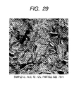
- FIG. 29 is an explanatory diagram showing an SEM photograph of a Ni 1 ⁇ y Pt y Si layer in a specimen No. 8 shown in FIG. 24 ,
- FIG. 30 is an explanatory diagram showing an SEM photograph of a Ni 1 ⁇ y Pt y Si layer in a specimen No. 6 shown in FIG. 24 ,
- FIG. 31 is an explanatory diagram showing an SEM photograph of a Ni 1 ⁇ y Pt y Si layer in a specimen No. 5 shown in FIG. 24 ,
- FIG. 32 is an explanatory diagram showing an SEM photograph of a Ni 1 ⁇ y Pt y Si layer in a specimen No. 7 shown in FIG. 24 ,
- FIG. 33 is a graph of the plot with alloy film consumption rates of the first heat treatment on the horizontal axis and with “concentrations of Pt” on the longitudinal direction about the specimens shown in the table of FIG. 24 ,
- FIG. 34 is a graph of the plot with alloy film consumption rates of the first heat treatment on the horizontal axis and with particle sizes on the longitudinal direction about the specimens shown in the table of FIG. 24 ,
- FIG. 35 is a graph of the plot with excess alloy film ratios on the horizontal axis and with concentrations of Pt on the longitudinal direction about the specimens shown in the table of FIG. 24 ,
- FIG. 36 is a graph of the plot with excess alloy film ratios of on the horizontal axis and with particle sizes on the longitudinal direction about the specimens shown in the table of FIG. 24 ,
- FIG. 37 is an explanatory diagram for explaining an increase in concentration of Pt
- FIG. 38 is an explanatory diagram for explaining an increase in concentration of Pt
- FIG. 39 is a graph showing the thickness of a reacted part of the alloy film in performing a heat treatment corresponding to the first heat treatment
- FIG. 40 is a graph showing the thickness of a reacted part of the alloy film in performing a heat treatment corresponding to the first heat treatment
- FIG. 41 is a graph showing the thickness of a reacted part of the alloy film in performing a heat treatment corresponding to the first heat treatment
- FIG. 42 is a graph showing the thickness of a reacted part of the alloy film in performing a heat treatment corresponding to the first heat treatment
- FIG. 43 is a cross-sectional view of a main part of the semiconductor device in the manufacturing procedure thereof (on the stage where the alloy film is formed) in the embodiment of the invention.
- FIG. 44 is a graph showing variations in resistance of a metal silicide layer when the metal silicide layer is formed
- FIG. 45 is a graph showing the number of leaks generated when the metal silicide layer is formed on a source/drain region of a MISFET
- FIG. 46 is a graph showing the number of leaks generated when the metal silicide layer is formed on a source/drain region of a MISFET
- FIG. 47A is an explanatory diagram showing one example of a heat treatment device used in the manufacturing procedure of the semiconductor device in the embodiment of the invention.
- FIG. 47B is an explanatory diagram showing one example of the heat treatment device used in the manufacturing procedure of the semiconductor device in the embodiment of the invention.
- FIG. 48A is an explanatory diagram of a susceptor included in the heat treatment device shown in FIGS. 47A and 47B ,
- FIG. 48B is an explanatory diagram of the susceptor included in the heat treatment device shown in FIGS. 47A and 47B ,
- FIG. 49 is a graph showing the thickness of a reacted part of the alloy film in performing a heat treatment corresponding to the first heat treatment
- FIG. 50 is a graph showing the thickness of a reacted part of the alloy film in performing a heat treatment corresponding to the first heat treatment
- FIG. 51 is a graph showing the thickness of a reacted part of the alloy film in performing a heat treatment corresponding to the first heat treatment
- FIG. 52 is a cross-sectional view of a main part of a semiconductor device in a manufacturing procedure of the semiconductor device according to another embodiment of the invention.
- FIG. 53 is a cross-sectional view of a main part of the semiconductor device in the manufacturing procedure thereof, following the step shown in FIG. 52 ,
- FIG. 54 is a cross-sectional view of a main part of the semiconductor device in the manufacturing procedure thereof, following the step shown in FIG. 53 ,
- FIG. 55 is a cross-sectional view of a main part of the semiconductor device in the manufacturing procedure thereof, following the step shown in FIG. 54 , and
- FIG. 56 is a cross-sectional view of a main part of the semiconductor device in the manufacturing procedure thereof, following the step shown in FIG. 55 .
- Preferred embodiments may be described by being divided into sections or embodiments for convenience, if necessary, but these embodiments are related to each other except when specified otherwise.
- One of the embodiments has a relationship with respect to the other so as to be a modified example of a part or all of the other, or a detailed part or a supplemental description of the other embodiment.
- the embodiments are not limited to a specific value except when specified otherwise and except when clearly limited otherwise in principle, and thus may be equal to or more than, or less than the specific value.
- components are not necessarily essential except when specified otherwise and except when clearly considered essential in principle.
- shapes, positional relations and the like of the components or the like in the following description of the embodiments they will include ones substantially analogous or similar to their shapes or the like, unless otherwise specified and considered not to be definitely so in principle. The same goes for the numeral value and range described above.
- a dry cleaning technique is disclosed in Japanese Patent Application No. 2006-107780 filed by Futase, et al. (on Apr. 10, 2006), and Japanese Patent Application No. 2007-81147 filed by Futase, et al. (on Mar. 27, 2007).
- FIGS. 1 to 5 are cross-sectional views showing main parts of the semiconductor device during the manufacturing procedure thereof device according to one embodiment of the invention, for example, the semiconductor device including a complementary metal insulator semiconductor field effect transistor (CMISFET).
- CMISFET complementary metal insulator semiconductor field effect transistor
- a semiconductor substrate (semiconductor wafer) 1 including a p-type single crystal silicon or the like having a specific resistance of, for example, about 1 to 10 ⁇ cm is prepared.
- Element isolation regions 2 are formed at a main surface of the semiconductor substrate 1 .
- the element isolation region 2 is formed of an insulator, such as silicon oxide, for example, by a shallow trench isolation (STI) method, or by a local oxidization of silicon method (LOCOS) method.
- STI shallow trench isolation
- LOC local oxidization of silicon method
- an insulating film embedded in a slot (element isolation slot) 2 a formed in the semiconductor substrate 1 can form the element isolation region 2 .
- a p-type well 3 and an n-type well 4 are formed in a predetermined depth from the main surface of the semiconductor substrate 1 .
- the p-type well 3 can be formed by ion implantation of p-type impurities, such as boron (B), into an n-channel MISFET formation area of the semiconductor substrate 1 using a photoresist film (not shown) covering a p-channel MISFET formation area as an ion implantation inhibition mask.
- p-type impurities such as boron (B)
- the n-type well 4 can be formed by ion implantation of n-type impurities, such as phosphorus (P) or arsenic (As), into a p-channel MISFET formation area of the semiconductor substrate 1 using another photoresist film (not shown) covering an n-channel MISFET formation area as an ion implantation inhibition mask.
- n-type impurities such as phosphorus (P) or arsenic (As
- the surface of the semiconductor substrate 1 is cleansed (cleaned), for example, by wet etching or the like using a hydrofluoric acid (Hf) solution, and a gate insulating film 5 is formed over the surface of the semiconductor substrate 1 (that is, on the p-type well 3 and the n-type well 4 ).
- the gate insulating film 5 is comprised of, for example, a thin silicon oxide film, and can be formed, for example, by thermal oxidation or the like.
- a silicon film 6 such as a polysilicon film, is formed over the semiconductor substrate 1 (that is, on the gate insulating film 5 on the p-type well 3 and the n-type well 4 ) as a conductive film for formation of a gate electrode.
- An n-channel MISFET formation area of the silicon film 6 (an area for a gate electrode GE 1 to be described later) becomes a low-resistance n-type semiconductor film (doped polysilicon film) formed by ion implantation of n-type impurities, such as phosphorus (P) or arsenic (As), using a photoresist film (not shown) as a mask.
- n-type impurities such as phosphorus (P) or arsenic (As)
- a p-channel MISFET formation area of the silicon film 6 (an area for a gate electrode GE 2 to be described later) becomes a low-resistance p-type semiconductor film (doped polysilicon film) formed by ion implantation of p-type impurities, such as boron (B), using another photoresist film (not shown) as a mask.
- the silicon film 6 which is an amorphous silicon film at the time of deposition can be converted into a polysilicon film by heat treatment after the deposition (ion implantation).
- the silicon film 6 is patterned by photolithography and dry etching to form gate electrodes GE 1 and GE 2 .
- the gate electrode GE 1 serving as a gate electrode of the n-channel MISFET is comprised of a polycrystal silicon (an n-type semiconductor film, or a doped polysilicon film) into which n-type impurities are introduced, and is formed over the p-type well 3 via the gate insulating film 5 . That is, the gate electrode GE 1 is formed on the gate insulating film 5 of the p-type well 3 .
- the gate electrode GE 2 serving as a gate electrode of the p-channel MISFET is comprised of a polycrystal silicon (a p-type semiconductor film or a doped polysilicon film) into which p-type impurities are introduced, and is formed over the n-type well 4 via the gate insulating film 5 . That is, the gate electrode GE 2 is formed on the gate insulating film 5 of the n-type well 4 .
- the gate length of each of the gate electrodes GE 1 and GE 2 can be changed as necessary, for example, to about 50 nm.
- n-type impurities such as phosphorus (P) or arsenic (As) are ion implanted into areas on both sides of the gate electrode GE 1 of the p-type well 3 to form (a pair of) n ⁇ -type semiconductor regions 7 a .
- p-type impurities such as boron (b) are ion implanted into areas on both sides of the gate electrode GE 2 of the n-type well 4 to form (a pair of) p ⁇ -type semiconductor regions 8 a .
- the depth (junction depth) of each of the n ⁇ -type semiconductor region 7 a and the p ⁇ -type semiconductor regions 8 a can be set, for example, to about 30 nm.
- a sidewall spacer or sidewall (sidewall insulating film) 9 comprised of, for example, a silicon oxide film, a silicon nitride film, or a lamination of these insulating films, is formed as a sidewall insulating film (insulating film) on each sidewall of the gate electrodes GE 1 and GE 2 .
- the sidewall 9 can be formed, for example, by depositing a silicon oxide film or a silicon nitride film or a lamination of these films over the semiconductor substrate 1 , and by anisotropic etching of the silicon oxide film or the silicon nitride film or the lamination of these films by a reactive ion etching (RIE) method.
- RIE reactive ion etching
- n-type impurities such as arsenic (As) or phosphorus (P) are ion implanted into areas on both sides of the gate electrode GE 1 of the p-type well 3 and the sidewalls 9 thereby to form (a pair of) n + -type semiconductor regions 7 b (source and drain).
- arsenic (As) ions are implanted at an acceleration voltage of 10 to 30 keV to a dose between about 1 ⁇ 10 15 /cm 2 and about 1 ⁇ 10 16 /cm 2 .
- arsenic (As) ions are implanted at an energy of 20 keV to a dose of 4 ⁇ 10 15 /cm 2 .
- phosphorus (P) ions are implanted at an acceleration voltage of 5 to 20 keV to a dose between about 1 ⁇ 10 14 /cm 2 and about 1 ⁇ 10 15 /cm 2 .
- phosphorus (P) ions are implanted at an acceleration voltage of 10 keV to a dose of 5 ⁇ 10 14 /cm 2 .
- the n + -type semiconductor region 7 b is formed.
- p-type impurities such as boron (B) are ion implanted into areas on both sides of the gate electrode GE 2 of the n-type well 4 and the sidewall 9 .
- boron (B) ions are implanted at an acceleration voltage of 1 to 3 keV to a dose between about 1 ⁇ 10 15 /cm 2 and about 1 ⁇ 10 16 /cm 2 .
- boron (B) ions are implanted at an acceleration voltage of 2 keV to a dose of 4 ⁇ 10 15 /cm 2 thereby to form the p + -type semiconductor region 8 b .
- Either one of the n + -type semiconductor region 7 b and the p + -type semiconductor region 8 b may be formed in advance.
- an anneal process for activating the impurities introduced is a spike anneal process at a temperature of, for example, about 1050° C.
- the depth (junction depth) of each of the n + -type semiconductor region 7 b and the p + -type semiconductor region 8 b can be, for example, about 80 nm.
- the n + -type semiconductor region 7 b has a higher concentration of impurities than that of the n ⁇ -type semiconductor region 7 a .
- the p + -type semiconductor region 8 b has a higher concentration of impurities than that of the p ⁇ -type semiconductor region 8 a .
- the n-type semiconductor region (impurity diffusion layer) serving as a source or drain of the n-channel type MISFET is formed of the n + -type semiconductor region (impurity diffusion layer) 7 b and the n ⁇ -type semiconductor region 7 a .
- the p-type semiconductor region (impurity diffusion layer) serving as a source or drain of the p-channel MISFET is formed of the p + -type semiconductor region (impurity diffusion layer) 8 b and the p ⁇ -type semiconductor region 8 a .
- the source/drain regions of the n-channel MISFET and the p-channel MISFET have a lightly doped drain (LDD) structure.
- the n ⁇ -type semiconductor region 7 a is formed in the gate electrode GE 1 in a self-alignment manner.
- the n + -type semiconductor region 7 b is formed against the sidewall 9 on each sidewall of the gate electrode GE 1 in a self-alignment manner.
- the p ⁇ -type semiconductor region 8 a is formed in the gate electrode GE 2 in a self-alignment manner.
- the p + -type semiconductor region 8 b is formed against the sidewall 9 formed on each sidewall of the gate electrode GE 2 in a self-alignment manner.
- an n-channel MISFET (metal insulator semiconductor field effect transistor) Qn is formed as a field-effect transistor in the p-type well 3 .
- a p-channel type MISFET (metal insulator semiconductor field effect transistor) Qp is formed as another field-effect transistor in the n-type well 4 .
- the n-channel MISFETQn can be defined as an n-channel field-effect transistor
- the p-channel MISFETQp can be defined as a p-channel field-effect transistor.
- the n + -type semiconductor region 7 b can be defined as a semiconductor region for the source or drain of the n-channel type MISFETQn.
- the p + -type semiconductor region 8 b can be defined as a semiconductor region for the source or drain of the p-channel type MISFETQp.
- a low-resistance metal silicide layer (corresponding to a metal silicide layer 41 b to be described later) is formed on the surfaces of the gate electrode GE 1 and of the source and drain regions (n + -type semiconductor regions 7 b ) of the n-channel MISFETQn, and on the surfaces of the gate electrode GE 2 and the source and drain regions (p + -type semiconductor region 8 b ) of the p-channel MISFETQp by a salicide (self aligned silicide) technique.
- a forming process of the metal silicide layer will be described below.
- FIG. 5 is a cross-sectional view of a main part in a manufacturing procedure of the semiconductor device, following the step shown in FIG. 4 .
- FIG. 6 is a manufacturing process flowchart showing a part of the manufacturing process of the semiconductor device in this embodiment.
- FIG. 6 shows a manufacturing process flow of a process for forming the metal silicide layer (metal and semiconductor reaction layer) on the surfaces of the gate electrodes GE 1 and GE 2 , the n + -type semiconductor region 7 b , and the p + -type semiconductor region 8 b by the silicide process after obtaining the structure shown in FIG. 4 .
- FIG. 7 is an exemplary plan view of a film forming device for silicide material (a material film for formation of the metal silicide layer, corresponding to the alloy film 11 and the barrier film 12 ).
- FIG. 8 is a diagram showing a deposition process (process flowchart) of silicide material.
- FIG. 9 is a schematic cross-sectional view showing a chamber for a dry cleaning process included in the deposition device of silicide material.
- FIG. 10 is a schematic cross-sectional view of a chamber for explaining process steps of a semiconductor wafer in the chamber for the dry cleaning process included in the deposition device of silicide material.
- FIGS. 11 to 15 are cross-sectional views of main parts of the semiconductor device in the manufacturing process thereof, following the step shown in FIG. 5 .
- FIG. 6 corresponds to a manufacturing process flow of the steps shown in FIGS. 5 , 11 , and 12
- FIG. 8 corresponds to a manufacturing process flow of the step shown in FIG. 5 .
- the surfaces of the gate electrodes GE 1 and GE 2 , the n + -type semiconductor region 7 b , and the p + -type semiconductor region 8 b are exposed after obtaining the structure shown in FIG. 4 as described above, and then an alloy film 11 is formed (deposited) using, for example, a sputtering method, over the main (entire) surface of the semiconductor substrate 1 containing the gate electrodes GE 1 and GE 2 , the n + -type semiconductor region 7 b , and the p + -type semiconductor region 8 b (in step S 1 shown in FIG. 6 ).
- step S 1 the alloy film 11 is formed over the semiconductor substrate 1 containing the surfaces of the n + -type semiconductor region 7 b and the p + -type semiconductor region 8 b to cover the gate electrodes GE 1 and GE 2 .
- a barrier film (a stress control film, an oxidation prevention film, and/or a cap film) 12 is formed (deposited) on the alloy film 11 (in step S 2 shown in FIG. 6 ).
- the dry cleaning process (corresponding to the step P 2 to be described later) is performed using at least one of HF gas, NF 3 gas, NH 3 gas, and H 2 gas thereby to remove a natural oxidation film on the surfaces of the gate electrodes GE 1 and GE 2 , the n + -type semiconductor region 7 b , and the p + -type semiconductor region 8 b .
- the steps S 1 and S 2 are more preferably performed without exposing the semiconductor substrate 1 to the atmosphere (under the atmosphere containing oxygen).
- the alloy film 11 is an alloy film (that is, a nickel alloy film) containing at least nickel (Ni), specifically, an alloy film containing nickel (Ni) and first metal element M, that is, a Ni-M alloy film.
- the first metal element M is at least one kind of element selected from the group consisting of Pt (platinum), Pd(palladium), V (vanadium), Er (erbium), and Yb (ytterbium), and more preferably Pt (platinum).
- the alloy film 11 is an alloy film containing nickel (Ni) and platinum (Pt), that is, a Ni—Pt alloy film.
- the alloy film 11 is more preferably a Ni—Pt alloy film (an alloy film containing Ni and Pt).
- the alloy film 11 can be represented as a Ni 1 ⁇ x M x alloy film, where M of Ni 1 ⁇ x M x is the first metal element M.
- the rate (ratio) of Ni in the Ni 1 ⁇ x M x alloy film is (1 ⁇ x) ⁇ 100%
- the rate (ratio) of the first metal element M in the Ni 1 ⁇ x M x alloy film is x ⁇ 100%.
- the rate (ratio, concentration) of the element in the present application is represented by atomic % in terms of %.
- a Ni 0.963 Pt 0.037 alloy film or the like can be used as the alloy film 11 .
- the rate (ratio) of Ni in the alloy film 11 is 96.3 atomic %
- the rate (ratio) of Pt in the alloy film 11 is 3.7 atomic %.
- the barrier film 12 is comprised of, for example, a titanium nitride (TiN) film or a titanium (Ti) film, and can have a thickness (thickness of deposition) of, for example, about 15 nm.
- the barrier film 12 acts as a stress control film (film for controlling stress in an active region of the semiconductor substrate), and a film for preventing penetration of oxygen.
- the barrier film 12 is provided on the alloy film 11 so as to control the stress applied to the semiconductor substrate 1 and to prevent oxidation of the alloy film 11 or the like. Now, one example of a preferred formation method of the alloy film 11 and the barrier 12 will be described below.
- the deposition of the alloy film 11 and the barrier film 12 is performed by a deposition device 20 of the silicide material shown in FIG. 7 .
- the deposition device 20 is of a multi-chamber type including two transfer chambers of a first transfer chamber 21 a and a second transfer chamber 21 b arranged therein with load lock chambers 23 and 24 and three chambers 25 , 26 , and 27 disposed around the first transfer chamber 21 a via gate valves 22 as opening and closing means, and with two chambers 28 and 29 disposed around the second transfer chamber 21 b via the gate valves 22 as the opening and closing means. Further, two chambers 30 and 31 for transfer are provided between the first transfer chamber 21 a and the second transfer chamber 21 b .
- the first transfer chamber 21 a is controlled such that a predetermined degree of vacuum is maintained by an exhaust mechanism or the like.
- the first transfer chamber 21 a is provided at its center with a robot 32 a for transfer with a multi-joined arm structure for transferring a semiconductor wafer SW.
- the second transfer chamber 21 b is controlled such that a predetermined degree of vacuum is maintained by an exhaust mechanism or the like. Further, the second transfer chamber 21 b is provided at its center with a robot 32 b for transfer with a multi-joined arm structure for transferring a semiconductor wafer SW.
- the chambers 25 and 26 included in the first transfer chamber 21 a is a chamber for heat treatment for performing the heat treatment at a relatively high temperature
- the chamber 27 is a chamber for the dry cleaning process (treatment).
- the chamber 28 included in the second transfer chamber 21 b is a chamber for deposition that is designed to form the alloy film 11 (preferably, a Ni—Pt alloy film) by the sputtering method
- the chamber 29 is a chamber for deposition that is designed to form the barrier film 12 (for example, a titanium nitride film) by the sputtering film.
- the chamber 29 is a chamber for deposition that is designed to form the barrier film 12 (for example, a titanium film) by the plasma CVD method.
- Each of the chambers 30 and 31 provided between the first transfer chamber 21 a and the second transfer chamber 21 b is a chamber for delivery that is designed to deliver the semiconductor wafer SW between the first transfer chamber 21 a and the second transfer chamber 21 b , and also a chamber for cooling that is used to cool the semiconductor wafer SW.
- the deposition device 20 has three chambers included only in the first transfer chamber 21 a , and two chambers included only in the second transfer chamber 21 b .
- the invention is not limited thereto, and any other chambers for the same application or for other applications can be added to the invention.
- one sheet of semiconductor wafer SW is taken out from any one of hoops 34 by a robot 36 for transfer disposed in a wafer transfer chamber 33 (in a process P 1 shown in FIG. 8 ) to be carried into either of the load lock chambers 23 and 24 .
- the semiconductor wafer SW corresponds to the above-mentioned semiconductor substrate 1 .
- the hoop 34 is a closed container for batch transfer of the semiconductor wafer SW.
- the hoop 34 normally accommodates therein 25, 12, and 6 pieces of semiconductor wafers SW in units of batch.
- An outer wall of the container of the hoop 34 is a sealed structure except for a fine vent filter, so that dust is mostly completely eliminated.
- FIG. 9 shows a schematic cross-sectional view of the chamber 27 . As shown in FIG.
- the chamber 27 mainly includes a wafer stage 27 a , wafer lift pins 27 b , a shower head 27 c , and a remote plasma generation device 27 d .
- the wafer stage 27 a and the wafer lift pin 27 b have independent elevating mechanisms that can arbitrarily control the distance between the shower head 27 c and the semiconductor wafer SW, and the distance between the semiconductor wafer SW and the wafer stage 27 a .
- the shower head 27 c disposed above the wafer stage 27 a is constantly maintained at a certain temperature, which is, for example, 180° C.
- the wafer stage 27 a is descended, and the wafer lift pins 27 b are ascended thereby to mount the semiconductor wafer SW on the wafer lift pins 27 b .
- the distance between the shower head 27 c and the semiconductor wafer SW is set to, for example, 16.5 ⁇ 12.7 mm, and the distance between the semiconductor wafer SW and the wafer stage 27 a is set to, for example, 25.4 ⁇ 17.8 mm.
- the wafer stage 27 a is ascended and the wafer lift pins 27 b are descended thereby to mount the semiconductor wafer SW on the wafer stage 27 a .
- the distance between the shower head 27 c and the semiconductor wafer SW is set to, for example, 17.8 ⁇ 5.1 mm.
- a remote plasma generator 27 d activates Ar gas with reducing gas, for example, NF 3 gas and NH 3 gas added thereto to generate plasma, which is introduced into the chamber 27 .
- a natural oxidation film is formed on the surface of silicon (a polycrystal silicon forming the gate electrodes GE 1 and GE 2 and a single crystal silicon forming the semiconductor substrate 1 with the n + -type semiconductor region 7 b and the p + -type semiconductor region 8 b formed therein).
- the natural oxidation film is removed by, for example, a reducing reaction caused between the natural oxidation film and the plasma and represented by the following formula (1).
- the process conditions of the dry cleaning process are, for example, a shower head temperature of 180° C., an NF 3 gas flow rate of 14 sccm, an NH 3 gas flow rate of 70 sccm, a pressure of 400 Pa, and a plasma power of 30 W.
- a product ((NH 4 ) 2 SiF 6 ) produced by the reducing reaction remains on the main surface of the semiconductor wafer SW.
- the semiconductor wafer SW is mounted only on the wafer stage 27 a , and the product remains at parts of the side and back surface of the semiconductor wafer SW.
- the product remaining at the parts of the side and back surface of the semiconductor wafer SW is peeled off in the case of transferring the semiconductor wafer SW to another chamber, which causes pollution or dust.
- the semiconductor wafer SW is subjected to the heat treatment in the chamber 27 , so that the product remaining on the main surface of the semiconductor wafer SW is removed, while the product remaining on the parts of the side and back surface of the semiconductor wafer SW is also removed.
- the wafer stage 27 a is descended and the wafer lift pins 27 b are ascended, so that the semiconductor wafer SW is got close to the shower head 27 c whose temperature is set to 180° C.
- the distance between the shower head 27 c and the semiconductor wafer SW is set to, for example, 3.8 ⁇ 2.6 mm, and the distance between the semiconductor wafer SW and the wafer stage 27 a is set to, for example, 5.9 mm or more.
- the semiconductor wafer SW is heated by use of a heating temperature (180° C.) of the shower head 27 c .
- the temperature of the semiconductor wafer SW ranges from 100 to 150° C.
- the product ((NH 4 ) 2 SiF 6 ) formed on the main surface of the semiconductor wafer SW sublimes, for example, based on the following formula (2) to be removed.
- the heat treatment heats the side and back surface of the semiconductor wafer SW to remove the product remaining on the parts of the side and back surface.
- the semiconductor wafer SW is transferred under vacuum from the chamber 27 for the dry cleaning process to the chamber 25 (or chamber 26 ) for the heat treatment via the first transfer chamber 21 a by the robot 32 a for transfer, and then put on a stage included in the chamber 25 (or the chamber 26 ) (in the process P 3 shown in FIG. 8 ).
- the semiconductor wafer SW is mounted on the stage of the chamber 25 (or chamber 26 ), and heated at a predetermined temperature thereby to sublime and remove the product remaining on the main surface of the semiconductor wafer SW without subliming the product at a temperature of 100 to 150° C.
- the temperature of the main surface of the semiconductor wafer SW is considered to be in an appropriate range of, for example, 150 to 400° C.
- the range of the temperature appropriate for mass production is preferably in a range of 165 to 350° C., and further most preferably in a range of 180 to 220° C., that is, in a range with 200° C. set as a center value.
- the semiconductor wafer SW is transferred under vacuum from the chamber 25 (or chamber 26 ) for the heating process to the chamber 30 (or chamber 31 ) for cooling and delivery via the first transfer chamber 21 a by the robot 32 a for transfer, and mounted on the stage included in the chamber 30 (or chamber 31 ) (in the process P 4 shown in FIG. 8 ).
- the semiconductor wafer SW is mounted on the stage of the chamber 30 (or chamber 31 ) and cooled.
- the semiconductor wafer SW is transferred under vacuum from the chamber 30 (or chamber 31 ) for cooling and delivery by the robot 32 b for transfer to the chamber 28 for deposition of the alloy film 11 via the second transfer chamber 21 b (in the process P 5 shown in FIG. 8 ).
- the semiconductor wafer SW is heated to a predetermined temperature, and the alloy film 11 (preferably, a Ni—Pt alloy film) is deposited on the main surface of the semiconductor wafer SW by the sputtering method, while introducing Ar gas into the chamber 28 at a predetermined flow rate.
- the deposition step of the alloy film 11 corresponds to the above step S 1 (step S 1 shown in FIG. 6 ).
- the thickness (deposition thickness) of the alloy film 11 is, for example, 25 nm.
- the sputtering conditions in deposition are, for example, a deposition temperature of 25° C., and an Ar gas flow rate of 35 sccm.
- the semiconductor wafer SW is transferred under vacuum from the chamber 28 for deposition of the alloy film 11 to the chamber 29 for deposition of the barrier film 12 via the second transfer chamber 21 b by the robot 32 b for transfer (in the process P 6 shown in FIG. 8 ).
- the semiconductor wafer SW is heated to a predetermined temperature, and the barrier film 12 of a titanium nitride film or the like is deposited on the main surface of the semiconductor wafer SW by the sputtering method, while introducing Ar gas and N 2 gas into the chamber 29 at a predetermined flow rate.
- the deposition step of the barrier film 12 corresponds to the above step S 2 (step S 2 shown in FIG. 6 ).
- the thickness (deposition thickness) of the barrier film 12 is, for example, 15 nm.
- the sputtering conditions in deposition are, for example, a deposition temperature of 40° C., an Ar gas flow rate of 28 sccm, and a nitride gas flow rate of 80 sccm.
- the semiconductor wafer SW is transferred under vacuum from the chamber 29 for deposition of the barrier 12 to the chamber 30 (or chamber 31 ) for cooling and delivery via the second transfer chamber 21 b by the robot 32 b for transfer (in the process P 7 shown in FIG. 8 ).
- the semiconductor wafer SW is transferred out from the chamber 30 (or chamber 31 ) for cooling and delivery to either of the load lock chambers 23 and 24 by the robot 32 a for transfer. Subsequently, the semiconductor wafer SW is returned to any one of the hoops 34 from the load lock chamber 23 or 24 via the wafer delivery device 33 by the robot 36 for transfer (in the process P 8 shown in FIG. 8 ).
- a remote plasma generator 27 d activates Ar gas (note that Ar gas is often used as gas for activation of plasma, but any other inert gas or a combined gas thereof may be used) with reducing gas, for example, NF 3 gas and NH 3 gas added thereto to generate plasma.
- the plasma is introduced into the chamber 27 to remove the natural oxidation film by the reducing reaction.
- the reducing gas such as HF gas and NH 3 gas, or NF 3 gas and NH 3 gas, may be introduced into the chamber 27 without plasma, thus removing the natural oxidation film by the reducing reaction.
- the deposition device is not limited to the remote plasma device, and the use of a normal plasma device is not problematic as long as other properties of the plasma device have no problems.
- the remote plasma has an advantage in no damage to the substrate.
- the invention is not limited to the above combination of gases, and even combinations of other gases that generate respective radicals or reaction species of nitrogen, hydrogen, and fluorine (including compound radicals thereof) may be used as long as they are not particularly harmful to this process.
- a mixture gas atmosphere of nitrogen, hydrogen, and fluorine radical generation gas (containing the mixture), plasma excitation gas, and the other additional gas and the like may be used appropriately.
- reaction gas such as the reducing gas
- the reaction gas is not limited to the above-mentioned gases, and any other gas for generating reaction species which reacts with an oxide film on a silicon surface at a relatively low temperature to vaporize may be used.
- a first heat treatment (annealing process) is applied to the semiconductor substrate 1 (in step S 3 shown in FIG. 6 ).
- the first heat treatment in step S 3 can be performed under ordinary pressure in an atmosphere of inert gas (for example, argon (Ar) gas, neon (Ne) gas, or helium (He) gas), or nitrogen (N 2 ) gas, or a mixture gas thereof.
- inert gas for example, argon (Ar) gas, neon (Ne) gas, or helium (He) gas
- nitrogen (N 2 ) gas or a mixture gas thereof.
- the first heat treatment can be carried out by, for example, a rapid thermal anneal (RTA) method.
- RTA rapid thermal anneal
- the polysilicon film forming the gate electrodes GE 1 and GE 2 selectively reacts with the alloy film 11
- the single-crystal silicon forming the n + -type semiconductor region 7 b and the p + -type semiconductor region 8 b selectively reacts with the alloy film thereby to form metal silicide layers 41 a which are metal-semiconductor reaction layers.
- An upper part (upper layer part) of each of the gate electrodes GE 1 and GE 2 , the n + -type semiconductor region 7 b , and the p + -type semiconductor region 8 b reacts with the alloy film 11 to form the metal silicide layer 41 a .
- the metal silicide layer 41 a is formed on each surface (upper layer part) of each of the gate electrodes GE 1 and GE 2 , the n + -type semiconductor region 7 b , and the p + -type semiconductor region 8 b.
- the metal silicide layer 41 a comprised of silicide containing nickel and the first metal element M is formed by selective reaction between the alloy film 11 and each of the gate electrodes GE 1 and GE 2 , the n + -type semiconductor region 7 b , and the p + -type semiconductor region 8 b (forming Si) by the first heat treatment in step S 3 .
- the metal silicide layer 41 a is in an (Ni 1 ⁇ y M y ) 2 Si phase (where 0 ⁇ y ⁇ 1).
- the “M” of a chemical formula of (Ni 1 ⁇ y M y ) 2 Si is the first metal element M.
- the metal silicide layer 41 a is comprised of a platinum-added nickel silicide layer in the (Ni 1 ⁇ y Pt y ) 2 Si phase (where 0 ⁇ y ⁇ 1).
- the first heat treatment is performed in step S 3 preferably at such a heat treatment temperature that forms the metal silicide layer 41 a in the (Ni 1 ⁇ y M y ) 2 Si phase without making a Ni 1 ⁇ y M y Si phase.
- the first heat treatment in step S 3 the Ni element and the first metal element M of the alloy film 11 are diffused into the n + -type semiconductor region 7 b , the p + -type semiconductor region 8 b , and the gate electrodes GE 1 and GE 2 , which forms the metal silicide layer 41 a .
- the first heat treatment is performed at a heat treatment temperature where a diffusion coefficient of the first metal element M into the n + -type semiconductor region 7 b , the p + -type semiconductor region 8 b , and the gate electrodes GE 1 and GE 2 is larger than that of Ni into the regions 7 b , 8 b , and the gate electrodes GE 1 and GE 2 .
- the first heat treatment is performed such that unreacted part of the alloy film 11 (corresponding to an unreacted part 11 a to be described later) remains on the metal silicide layer 41 a .
- the rate of the first metal element M included in metal elements (Ni and first metal element M) forming the thus-formed metal silicide layer 41 a is larger than that of the first metal element M in the alloy metal film 11 . This will be described later in detail.
- the barrier film 12 is a film that is less prone to react with the alloy film 11 .
- the barrier film 12 is desirably a film that does not react with the alloy film 11 even after the first heat treatment in step S 3 , and is preferably a titanium nitride (TiN) film or a titanium (Ti) film from this point of view.
- TiN titanium nitride
- Ti titanium
- the barrier film 12 as an oxidation prevention film may be omitted.
- the barrier film 12 and the unreacted part of the alloy film 11 are removed by the wet cleaning process (in step S 4 shown in FIG. 6 ).
- the non-reacted parts of the alloy film 11 are removed from the metal silicide layers 41 a , while leaving the metal silicide layers 41 a on the surfaces of the gate electrodes GE 1 and GE 2 , the n + -type semiconductor region 7 b , and the p + -type semiconductor region 8 b .
- the wet cleaning process in step S 4 can be performed by wet cleaning using sulfuric acid, or by wet cleaning using a mixture of sulfuric acid and a hydrogen peroxide solution.
- FIG. 11 shows the stage where the barrier film 12 and the unreacted parts of the alloy film 11 are removed by the wet cleaning process in step S 4 .
- the second heat treatment (anneal treatment) is applied to the semiconductor substrate 1 (in step S 5 shown in FIG. 6 ).
- the second heat treatment in step S 5 can be performed under ordinary pressure in an atmosphere of inert gas (for example, argon (Ar) gas, neon (Ne) gas, or helium (He) gas) or nitrogen (N 2 ) gas or a mixture gas thereof.
- inert gas for example, argon (Ar) gas, neon (Ne) gas, or helium (He) gas
- N 2 nitrogen
- the second heat treatment can be carried out by, for example, the rapid thermal anneal (RTA) method.
- the second heat treatment in step S 5 is performed at a heat treatment temperature higher than that of the first heat treatment in step S 3 described above.
- the second heat treatment in step S 5 is performed for decreasing a resistance of the metal silicide layer 41 a and stabilizing the silicide layer 41 a .
- the metal silicide layer 41 a in the (Ni 1 ⁇ y M y ) 2 Si phase formed by the first heat treatment in step S 3 is changed into the metal silicide layer 41 b in a Ni 1 ⁇ y M y Si phase.
- the stable metal silicide layer 41 b is formed in which a ratio of metal elements (including Ni with the first metal element M added thereto) to Si is very close to a stoichiometric proportion of 1:1.
- the metal silicide layers 41 a in the (Ni 1 ⁇ y M y ) 2 Si phase further react with silicon of the gate electrodes GE 1 and GE 2 , the n + -type semiconductor region 7 b , and the p + -type semiconductor region 8 b by the second heat treatment in step S 5 , so that the metal silicide layer 41 b having the low-resistance Ni 1 ⁇ y M y Si phase which is more stable than the (Ni 1 ⁇ y M y ) 2 Si phase is formed on the surfaces (upper layer parts) of the gate electrodes GE 1 and GE 2 , the n + -type semiconductor region 7 b , and the p + -type semiconductor region 8 b .
- the second heat treatment in step S 5 needs to be performed at such a temperature that can change the metal silicide layer 41 a in the (Ni 1 ⁇ y M y ) 2 Si phase into the metal silicide layer 41 b in the Ni 1 ⁇ y M y Si phase.
- the second heat treatment in step S 5 is preferably performed at such a heat treatment temperature that forms the metal silicide layer 41 b in the Ni 1 ⁇ y M y Si phase and not in the Ni 1 ⁇ y M y Si 2 phase.
- the Ni 1 ⁇ y M y Si phase has a resistivity lower than those of a (Ni 1 ⁇ y M y ) 2 Si phase and a Ni 1 ⁇ y M y Si 2 phase, and the metal silicide layer 41 b remains in the Ni 1 ⁇ y M y Si phase having the low resistance also in steps following the step S 5 (until the end of manufacturing of the semiconductor device).
- the metal silicide layer 41 b is still in the Ni 1 ⁇ y M y Si phase having the low resistance.
- the character “M” in the above-mentioned chemical formulas (Ni 1 ⁇ y M y ) 2 Si, Ni 1 ⁇ y M 1 ⁇ y Si, and Ni 1 ⁇ y M y Si 2 is the above first metal element M.
- the metal film 11 is a Ni—Pt alloy film (that is, when the first metal element M is Pt)
- the metal silicide layer 41 a formed by the first heat treatment in step S 3 has the (Ni 1 ⁇ y Pt y ) 2 Si phase.
- This layer is changed into the metal silicide layer 41 b having the Ni 1 ⁇ y Pt y Si phase by the second heat treatment in step S 5 .
- the Ni 1 ⁇ y PtySi phase has a lower resistivity than those of the (Ni 1 ⁇ y Pt y ) 2 Si phase and Ni 1 ⁇ y M y Si 2 phase.
- the metal silicide layer 41 b maintains the low-resistant Ni 1 ⁇ y Pt y Si phase.
- the metal silicide layer 41 b is still in the Ni 1 ⁇ y Pt y Si phase having a low resistance.
- the metal silicide layers 41 b in the Ni 1 ⁇ y M y Si phase are formed on the surfaces (upper layer parts) of the n-channel MISFETQn GE 1 and the source/drain region (n + -type semiconductor region 7 b ), and the surfaces (upper layer parts) of the gate electrode GE 2 of the p-channel MISFETQp and the source/drain region (p + -type semiconductor region 8 b ).
- an insulating film 42 is formed over the main surface of the semiconductor substrate 1 . That is, the insulating film (first insulating film) 42 is formed over the semiconductor substrate 1 including the metal silicide layer 41 b so as to cover the gate electrodes GE 1 and GE 2 , and the sidewalls 9 .
- the insulating film 42 is comprised of, for example, a silicon nitride film, and can be formed by the plasma CVD method at a deposition temperature (temperature of the substrate) of about 450° C.
- an insulating film 43 which is thicker than the insulating film 42 is formed on the insulating film 42 .
- the insulating film 43 is comprised of, for example, a silicon oxide film or the like.
- the insulating film 43 can be formed by the plasma CVD method at a deposition temperature of about 400° C. using a tetraethoxysilane or a tetra ethyl ortho silicate.
- an interlayer insulating film comprised of an insulating film 42 and an insulating film 43 is formed.
- the surface of the insulating film 43 is polished by a CMP method, resulting in planarized upper surface of the insulating film 43 .
- the interlayer insulating film with a planarized surface can be obtained by polishing the surface of the insulating film 43 by the CMP method.
- the insulating films 43 and 42 are dry-etched using a photoresist pattern (not shown) formed on the insulating film 43 as an etching mask thereby to form contact holes (through holes, or holes) 44 in the insulating films 42 and 43 .
- the insulating film 43 is dry etched on conditions where the insulating film 43 is easily etched as compared to the insulating film 42 , while the insulating film 42 serves as an etching stopper film, so that contact holes 44 are formed in the insulating film 43 .
- the part of the insulating film 42 located at the bottom of each contact hole 44 is dry etched and removed on conditions where the insulating film 42 is easily etched as compared to the insulating film 43 .
- parts of the main surface of the semiconductor substrate 1 for example, parts of the metal silicide layers 41 b on the surfaces of the n + -type semiconductor region 7 b and the p + -type semiconductor region 8 b , and parts of the metal silicide layers 41 b on the surfaces of the gate electrodes GE 1 and GE 2 , are exposed.
- conductive plugs (conductors for connection) 45 including tungsten (w) or the like are formed in the contact holes 44 .
- a barrier conductive film 45 a (for example, a titanium film, a titanium nitride film, or a lamination thereof) is formed on the insulating film 43 covering the inside of the contact hole 44 (bottom and side walls) by the plasma CVD method at a deposition temperature (temperature of the substrate) of about 450° C.
- the main conductive film 45 b formed of a tungsten film or the like is formed over the barrier conductive film 45 a by the CVD method so as to fill the contact hole 44 therewith, and unnecessary parts of the main conductive film 45 b and the barrier conductive film 45 a on the insulating film 43 are removed by the CMP method or etch back method, so that the plugs 45 can be formed.
- the plug 45 formed on the gate electrode GE 1 or GE 2 , the n + -type semiconductor region 7 b , or the p + -type semiconductor region 8 b is electrically coupled at its bottom to the metal silicide layer 41 b on the surface of the gate electrode GE 1 or GE 2 , the n + -type semiconductor region 7 b , or the p + -type semiconductor region 8 b.
- a stopper insulating film (an insulating film for an etching stopper) 51 and an insulating film 52 for formation of wiring are formed in turn over the insulating film 43 with the plugs 45 embedded therein.
- the stopper insulating film 51 is a film serving as an etching stopper in processing slots in the insulating film 52 .
- the stopper insulating film 51 in use includes a material having adequate etching selectivity with respect to the insulating film 52 .
- the stopper insulating film 51 can be formed, for example, of a silicon nitride film by the plasma CVD method.
- the insulating film 52 can be formed, for example, of a silicon oxide film formed by the plasma CVD method. It is noted that the stopper insulating film 51 and the insulating film 52 are provided with a first layer wiring to be described later.
- the first layer wiring is formed by a single-damascene method.
- wiring slots 53 are formed in respective predetermined areas of the insulating film 52 and the stopper insulating film 51 by the dry etching using a resist pattern (not shown) as a mask.
- a conductive barrier film (barrier metal film) 54 is formed over the main surface of the semiconductor substrate 1 (that is, on the surface of the insulating film 52 containing the bottom and side wall of each wiring slot).
- the conductive barrier film 54 in use can be, for example, a titanium nitride film, a tantalum film, or a tantalum nitride film.
- a copper seed layer is formed on the conductive barrier film 54 by the CVD method or sputtering method, and a copper plating film is formed on the seed layer using electrolytic plating or the like.
- the inside of the wiring slot 53 is filled with a copper plating film.
- the copper plating film, the seed layer, and the barrier metal film 54 located in areas other than the wiring slots 53 are removed by the CMP method thereby to form the first-layer wiring 55 containing copper as a principal conductive material.
- the wirings 55 are electrically coupled to the n + -type semiconductor region 7 b and the p + -type semiconductor region 8 b , and the gate electrodes GE 1 and GE 2 , and the like for the source or drain of the n-channel MISFETQn and the p-channel MISFETQp via the plugs 45 . Thereafter, wirings of a second or later layer are formed by a dual damascene method. Here, the wirings are not shown and a description thereof will be omitted.
- step S 3 the first heat treatment in step S 3 and the second heat treatment in step S 5 will be further described in detail below.
- FIGS. 16 to 21 show cross-sectional views of main parts of the semiconductor device in the manufacturing process thereof on the respective stages of steps S 1 , S 2 , S 3 , S 4 , and S 5 , each showing an area around an upper part of a silicon (Si) region 61 .
- FIG. 22 is a graph showing diffusion coefficients of Ni and Pt in a Si region (silicon region), while showing Arrhenium plots of the diffusion coefficients of Ni and Pt in the Si region.
- the longitudinal axis in the graph of FIG. 22 corresponds to the diffusion coefficient of Ni or Pt in the Si region, and the horizontal axis in FIG. 22 corresponds a value obtained by multiplying the inverse of an absolute temperature T by 1000 times.
- FIGS. 16 to 21 FIG.
- FIG. 16 shows the stage directly before the alloy film 11 is formed in step S 1 .
- FIG. 17 shows the stage where the alloy film 11 is formed by performing the process in step S 1 (the stage before formation of the barrier film 12 in step S 2 ).
- FIG. 18 shows the stage where the barrier film 12 is formed by performing the process in step S 2 (the stage before formation of the first heat treatment in step S 3 ).
- FIG. 19 shows the stage where the first heat treatment is performed in step S 3 (on the stage before a removing step S 4 of removing the barrier film 12 and an unreacted part of the alloy film 11 ).
- FIG. 20 shows the stage of step S 4 where the removing step of the barrier film 12 and the unreacted part of the alloy film 11 is performed (on the stage before a second heat treatment of step S 5 is performed).
- FIG. 21 shows the stage of step S 5 where the second heat treatment is performed (the stage before the formation of the insulating film 42 ).
- the silicon region 61 shown in FIGS. 16 to 21 corresponds to any one of the gate electrode GE 1 and GE 2 , the n + -type semiconductor region 7 b and the p + -type semiconductor region 8 b .
- any one of the gate electrode GE 1 and GE 2 , the n + -type semiconductor region 7 b , and the p + -type semiconductor region 8 b is comprised of a silicon region (specifically, while each of the gate electrodes GE 1 and GE 2 is formed of a polysilicon film, and each of the n + -type semiconductor region 7 b and the p + -type semiconductor region 8 b is formed of a single crystal silicon region).
- the silicon region 61 is the gate electrode GE 1 or gate electrode GE 2 , the silicon region 61 is comprised of polycrystal silicon.
- the silicon region 61 is formed of the n + -type semiconductor region 7 b or the p + -type semiconductor region 8 b , the silicon region 61 is comprised of single crystal silicon.
- the alloy film 11 is formed over the main surface (entire surface) of the semiconductor substrate 1 including the silicon region 61 (that is, the gate electrodes GE 1 and GE 2 , and the n + -type semiconductor region 7 b , and the p + -type semiconductor region 8 b ) in step S 1 .
- the formation thickness (deposition thickness) of the alloy film 11 at the silicon region 61 is a thickness (film thickness, or first thickness) tn 1 .
- the thickness tn 1 corresponds to the thickness of the alloy film 11 on the silicon region 61 before the first heat treatment in step S 3 .
- the formed alloy film 11 is an Ni 1 ⁇ x M x alloy film (where 0 ⁇ x ⁇ 1) in which the atomic ratio of Ni to the first metal element M is 1 ⁇ x:x.
- step S 2 the barrier film 12 is formed on the alloy film 11 .
- step S 3 the silicon region 61 reacts with the alloy film 11 thereby to form the metal silicide layer 41 a in the (Ni 1 ⁇ y Pt y ) 2 Si phase (where 0 ⁇ y ⁇ 1) on the surface (upper layer part) of the silicon region 61 .
- the first heat treatment is performed in step S 3 such that the unreacted part 11 a of the alloy film 11 remains on the metal silicide layer 41 a without causing the entire alloy film 11 on the silicon region 61 to react with the silicon region 61 .
- the unreacted part 11 a corresponds to a part not reacted with the silicon region 61 by the first heat treatment in step S 3 , in the alloy film 11 positioned above the silicon region 61 before the first heat treatment in step S 3 .
- the thickness of the unreacted part 11 a still remaining at the silicon region 61 after the first heat treatment in step S 3 (before the step of removing the barrier film 12 and the unreacted alloy film 11 in step S 4 ) in the alloy film 11 positioned on the silicon region 61 is a thickness (film thickness, or third thickness) tn 2 .
- the thickness of the formed metal silicide layer 41 a is a thickness tn 4 .
- FIG. 18 illustrates the unreacted part 11 a and a reacted part 11 b of the alloy film divided into by a dummy line indicated by a dotted line.
- the reacted part 11 b corresponds to a part with the metal silicide layer 41 a formed in reaction with the silicon region 61 by the first heat treatment in step S 3 , among the alloy film 11 positioned above the silicon region 61 before the first heat treatment in step S 3 .
- a combination of the reacted part 11 b and the unreacted part 11 a corresponds to the alloy film 11 positioned above the silicon region 61 before the first heat treatment in step S 3 .
- the alloy film 11 is actually a single layer with a lower layer part of the alloy film 11 as the reacted part 11 b and an upper layer part of the alloy film 11 as the unreacted part 11 a .
- the reacted part 11 b and the unreacted part 11 a substantially correspond to two areas of the alloy film 11 substantially divided into in the form of layer (the lower area corresponding to the reacted part 11 b , and the upper area corresponding to the unreacted part 11 a ).
- the thickness of the reacted part 11 b is a thickness (second thickness) tn 3
- the first heat treatment in step S 3 is performed such that the unreacted part 11 a of the alloy film 11 remains on the metal silicide layer 41 a in the form of layer.
- the thickness tn 3 of the reacted part 11 b of the alloy film 11 is smaller than the thickness tn 1 of the alloy film 11 on the silicon region 61 before the first heat treatment (tn 3 ⁇ tn 1 ), and the thickness tn 2 of the unreacted part 11 a of the alloy film 11 remaining on the metal silicide layer 41 a after the first heat treatment is larger than zero (tn 2 >0).
- the barrier film 12 and the unreacted part of the alloy film 11 are removed in step S 4 .
- the unreacted part 11 a on the metal silicide layer 41 a is also removed. Therefore, the second heat treatment is performed in step S 5 to cause the metal silicide layer 41 a in the (Ni 1 ⁇ y M y ) 2 Si phase to further react with the silicon region 61 , so that the metal silicide layer 41 b in the Ni 1 ⁇ y M y Si phase is formed on the surface (upper layer part) of the silicon region 61 as shown in FIG. 21 .
- the thickness of the formed metal silicide layer 41 b is a thickness tn 5 .
- the first heat treatment in step S 3 has the features to satisfy the following two conditions (the first condition and the second condition).
- the first heat treatment is performed in step S 3 at such a heat treatment temperature T 1 that a diffusion coefficient of the first metal element M (preferably, Pt) into the silicon region 61 (the gate electrodes GE 1 and GE 2 , the n + -type semiconductor region 7 b , and the p + -type semiconductor region 8 b ) becomes larger than that of nickel (Ni) into the silicon region 61 (the gate electrodes GE 1 and GE 2 , the n + -type semiconductor region 7 b , and the p + -type semiconductor region 8 b ).
- a diffusion coefficient of the first metal element M preferably, Pt
- the diffusion coefficient of the first metal element M (preferably, Pt) is larger than that of nickel (Ni).
- the first metal element M (preferably, Pt) is more easily diffused from the alloy film 11 into the silicon region 61 than nickel (Ni) in the first heat treatment in step S 3 .
- FIG. 22 shows a graph of dependence of diffusion coefficients of Ni and Pt in the Si region (silicon region) on temperature. As shown in the graph of FIG. 22 , both diffusion coefficients of Ni and of Pt increase with increasing temperature, but the Ni and Pt elements differ from each other in temperature dependence of the diffusion coefficient. Thus, the graph of FIG. 22 shows that at a temperature higher than the temperature T 2 , the diffusion coefficient of Ni in the Si region is larger than that of Pt in the Si region, whereby Ni is more easily diffused into the Si region than Pt. At the temperature T 2 , the diffusion coefficient of Ni into the Si region is the same as that of Pt into the Si region, so that the diffusivity of Ni into the Si region is the same as that of Pt.
- the diffusion coefficient of Pt into the Si region is larger than that of Ni into the Si region, whereby Pt is more easily diffused into the Si region than Ni.
- the heat treatment temperature T 1 of the first heat treatment in step S 3 is set lower than the above-mentioned T 2 (that is, T 1 ⁇ T 2 ) in order to satisfy the first condition.
- the heat treatment temperature T 1 of the first heat treatment in step S 3 is less than 279° C. (that is, T 1 ⁇ 279° C.).
- the diffusion coefficient of Pt (platinum) into the silicon region 61 becomes larger than that of nickel (Ni) into the silicon region 61 at the heat treatment temperature T 1 of the first heat treatment in step S 3 .
- Pt (platinum) is more easily diffused than Ni (nickel) from the alloy film 11 into the silicon region 61 (the gate electrodes GE 1 and GE 2 , the n + -type semiconductor region 7 b , and the p + -type semiconductor region 8 b ).
- the first heat treatment in step S 3 is performed such that the unreacted part 11 a of the alloy film 11 remains on the metal silicide layer 41 a (that is, tn 1 >tn 2 >0).
- the reaction rate R 1 of the alloy film 11 to the silicon region 61 is less than 100%.
- the upper layer part of the alloy film 11 positioned above the silicon region 61 (the gate electrodes GE 1 and GE 2 , the n + -type semiconductor region 7 b , and the p + -type semiconductor region 8 b ) remains on the metal silicide layer 41 a as the unreacted part 11 a as it is even after the first heat treatment in step S 3 .
- the first heat treatment in step S 3 leaves the unreacted part 11 a of the alloy film 11 on the metal silicide layer 41 a.
- the reaction rate R 1 of reaction between the alloy film 11 and the silicon region 61 corresponds to the rate of the part (that is, reacted part 11 b ) having the metal silicide layer 41 a formed therein by reaction with the silicon region 61 by the first heat treatment in step S 3 in the alloy film 11 positioned above the silicon region 61 .
- the reaction rate R 1 of reaction between the alloy film 11 and the silicon region 61 corresponds to the thickness of the alloy film 11 consumed for forming the metal film 41 a in the first heat treatment in step S 3 , that is, the thickness tn 2 of the reacted part 11 b , with respect to the thickness tn 1 of the alloy film 11 before the first heat treatment in step S 3 .
- the Ni element and the first metal element M forming the alloy film 11 are diffused from the alloy film 11 into the silicon region 61 thereby to form the metal silicide layer 41 a .
- the first metal element M preferably, Pt
- the first metal element M is more easily diffused into the silicon region 61 than Ni.
- an atomic number ratio of the Ni element to the first metal element M diffused from the alloy film 11 into the silicon region 61 maintains an original atomic number ratio of the Ni element to the first metal element M forming the alloy film 11 .
- an atomic number ratio of the Ni element to the first metal element M in the metal silicide layer 41 a maintains the original atomic number ratio of the Ni element to the first metal element M forming the alloy film 11 .
- the first heat treatment is performed so as to satisfy the first condition and the second condition. Since the first metal element M is more easily diffused into the silicon region 61 than the Ni element in the first heat treatment, the atomic number ratio of the Ni element to the first metal element M diffused from the alloy film 11 into the silicon region 61 is one in which the rate of the first metal element M is increased as compared to the atomic number ratio of the Ni element to the first metal element M forming the alloy film 11 .
- the atomic number ratio of the Ni element to the first metal element M in the metal silicide layer 41 a is also one in which the rate of the first metal element M is increased as compared to the atomic number ratio of the Ni element to the first metal element M forming the alloy film 11 .
- the alloy film 11 is the Ni 1 ⁇ x M x alloy film (where 0 ⁇ x ⁇ 1)
- the metal silicide layer 41 a is in the (Ni 1 ⁇ y M y ) 2 Si phase (where 0 ⁇ y ⁇ 1)
- the following relationship is obtained: x ⁇ y.
- the first heat treatment in step S 3 satisfies the first condition and does not satisfy the second condition with the reaction rate R 1 of reaction between the alloy film 11 and the silicon region 61 being 100%
- the Ni element and the first metal element M forming the alloy film 11 on the silicon region 61 are entirely diffused into the silicon region 61 to contribute to formation of the metal silicide layer 41 a regardless of a difference in diffusion coefficient between these elements.
- the first metal element M is more easily diffused into the silicon region 61 than the Ni element, all amounts of the Ni element and the first metal element M forming the alloy film 11 on the silicon region 61 react with the silicon region 61 to form the metal silicide layer 41 a .
- the first heat treatment satisfying the above second condition and not satisfying the first condition is performed in step S 3 at such a heat treatment temperature that makes the diffusion coefficient of Ni into the silicon region 61 larger than the diffusion coefficient of the first metal element M into the silicon region 61 .
- the Ni element is diffused into the silicon region 61 ahead of the first metal element M, which may decrease the rate of the first metal element M in the metal silicide layer 41 a . That is, the formation of the metal silicide layer 41 a in the (Ni 1 ⁇ y M y ) 2 S phase using the Ni 1 ⁇ x M x alloy film as the alloy film 11 results in y ⁇ x.
- the first heat treatment is performed in step S 3 so as to satisfy both the first condition and the second condition, whereby the rate of the first metal element M (preferably, Pt) with respect to the metal silicide layer 41 a can be enhanced. That is, both the first condition and the second condition are satisfied, so that the rate of the first metal element M included in metal elements forming the metal silicide layer 41 a (the sum of the Ni and first metal element M) can be larger than the rate of the first metal element M included in the alloy film 11 .
- the rate of the first metal element M preferably, Pt
- both the first condition and the second condition are satisfied, so that the formation of the metal silicide layer 41 a in the (Ni 1 ⁇ y M y ) 2 S phase (where M is preferably Pt) using the Ni 1 ⁇ x M x alloy film (where M is preferably Pt) as the alloy film 11 can result in x ⁇ y.
- the alloy film 11 containing the Ni element and the first metal element M reacts with the silicon region 61 to form the metal silicide layer 41 a
- the metal elements forming the metal silicide layer 41 a are the same as those forming the alloy film 11 , specifically, the Ni element and the first metal element M.
- both the metal silicide layer 41 a in the (Ni 1 ⁇ y M y ) 2 Si phase and the metal silicide layer 41 b in the Ni 1 ⁇ y M y Si phase maintain the same ratio of the Ni element to the first metal element M (that is, 1 ⁇ y:y).
- the character y of the (Ni 1 ⁇ y M y ) 2 Si forming the metal silicide layer 41 a takes the same value as the character y of the Ni 1 ⁇ y M y Si forming the metal silicide layer 41 b.
- addition of the first metal element M (in particular, preferably, Pt) to the nickel silicide layer can have the advantages in less agglomeration of the formed metal silicide layer, and in suppression of abnormal growing of a high-resistance NiSi 2 phase in the formed metal silicide layer, thus enabling improvement of the reliability of the semiconductor device.
- the Ni element differs from the first metal element M in sputtering angle in depositing the Ni 1 ⁇ x M x alloy film on the semiconductor substrate, an increase in concentration of the first metal element M in the Ni 1 ⁇ x M x alloy film can result in a nonuniform Ni 1 ⁇ x M x alloy film formed on the semiconductor substrate. This phenomenon is remarkable especially when the first metal element M is Pt.
- the concentration of the first metal element M that is, x of the Ni 1 ⁇ x M x
- the concentration of the first metal element M is increased by adjusting a sputtering angle of the first metal element M using a honeycomb collimator or the like so as to uniformly deposit the Ni 1 ⁇ x M x alloy film on the semiconductor substrate
- the Ni 1 ⁇ x M x alloy film may be much deposited over the collimator.
- the effect obtained by addition of the first metal element M (in particular, preferably, Pt) into the above-mentioned nickel silicide layer is enhanced as increasing concentration of the first metal element M (in particular, preferably, Pt) in the nickel silicide layer.
- the first heat treatment is performed in step S 3 so as to satisfy both the first condition and the second condition, whereby the rate of the first metal element M (that is, corresponding to the value of the character y when the metal silicide layer 41 a is represented as the (Ni 1 ⁇ y M y ) 2 Si alloy film) included in metal elements forming the metal silicide layer 41 a can be enhanced (that is, y>x) as compared to the rate of the first metal element M included in the alloy film 11 (that is, corresponding to the character x when the alloy film 11 is represented as Ni 1 ⁇ x M x alloy film).
- the rate of the first metal element M included in the metal elements forming the metal silicide layer 41 b (that is, corresponding to the character y when the metal silicide layer 41 b is represented as Ni 1 ⁇ y M y Si alloy film) can be enhanced (that is, y>x) as compared to the rate of the first metal element M included in the alloy film 11 (that is, corresponding to the value of the character x when the alloy film 11 is represented as Ni 1 ⁇ x M x alloy film).
- agglomeration of the metal silicide layers 41 a and 42 can be suppressed, and abnormal growing of the high-resistance Ni 1 ⁇ y M y Si 2 phase can be suppressed in the metal silicide layer 41 b , which can improve the reliability of the semiconductor device.
- FIG. 23 is a graph showing a specific resistance of the metal silicide layer 41 b when the metal silicide layer 41 a is formed as the alloy film 11 using Ni 0.963 Pt 0.037 alloy film.
- the longitudinal axis of the graph corresponds to a specific resistance of the metal silicide layer 41 b
- the horizontal axis of the graph corresponds to an alloy film consumption rate R 2 in the first heat treatment.
- the thickness tn 6 of the alloy film 11 consumable (reactable with the silicon region 61 ) in the first heat treatment corresponds to the thickness of a part reacted with the silicon region 61 by the first heat treatment (that is, thickness tn 3 of the reacted part 11 b ) when the thickness tn 1 of the alloy film 11 is sufficiently thick (as compared to the thickness tn 6 ).
- the first heat treatment is performed on the alloy film 11 having the thickness tn 1 of 10 ⁇ m under the same heat treatment conditions as the case of the reacted part 11 b of the alloy film 11 having the thickness tn 3 of 20 ⁇ m which is obtained by forming the alloy film 11 in the thickness tn 1 of 40 ⁇ m and by applying the first heat treatment thereto.
- tn 6 20 ⁇ m
- tn 1 10 ⁇ m.
- the alloy film consumption rate R 2 of the first heat treatment is 200%
- the reaction rate R 1 of the first heat treatment is 100%.
- the same heat treatment conditions include at least the same heat treatment temperature and heat treatment time.
- the graph of FIG. 23 is the plot obtained under the mixtures of different heat treatment temperatures and heat treatment times of the first heat treatment, while the first heat treatment constantly satisfies the above first condition.
- the alloy film consumption rate R 2 of the first heat treatment is less than 100%, the above second condition is satisfied.
- the alloy film consumption rate R 2 of the first heat treatment is equal to or more than 100%, the above second condition is not satisfied.
- the graph of FIG. 23 shows the following facts.
- the metal silicide layer 41 b has a low resistivity and is in the Ni 1 ⁇ y M y Si phase, specifically, Ni 1 ⁇ y Pt y Si phase.
- the resistivity of the metal silicide layer 41 b is increased. This is because a Ni 1 ⁇ y M y Si 2 phase having a high resistivity, specifically, Ni 1 ⁇ y Pt y Si 2 phase is abnormally grown in the metal silicide layer 41 b.
- the resistivity of the metal silicide layer 41 b is substantially constant.
- the resistivity of the metal silicide layer 41 b is decreased as decreasing alloy film consumption rate R 2 in the first heat treatment. This is based on the following reason.
- the first heat treatment satisfies the first condition and the second condition as described above, which enhances the rate of the first metal element M (here, Pt) in the metal silicide layer 41 b . That is, the value of the character “y” provided when the metal silicide layer 41 a is represented as the Ni 1 ⁇ y M y Si alloy film, specifically, Ni 1 ⁇ y Pt y Si in this embodiment is enhanced.
- Ni 1 ⁇ y M y Si alloy film decreases its resistivity as increasing value of y of, especially, Ni 1 ⁇ y Pt y Si material.
- the rate of the first metal element M (specifically, Pt in this embodiment) in the metal silicide layer 41 b is enhanced (that is, the value of y in the (Ni 1 ⁇ y M y ) Si becomes large) with decreasing alloy film consumption rate R 2 of the first heat treatment, which reduces the resistivity of the metal silicide layer 41 b.
- the first heat treatment is performed in step S 3 so as to satisfy the first condition and the second condition thereby to enhance the rate of the first metal element M (preferably, Pt) in the formed metal silicide layer 41 b , which can further reduce the resistivity of the metal silicide layer 41 b.
- the first metal element M preferably, Pt
- FIG. 24 is a table showing a summary of various conditions where the Ni 1 ⁇ y Pt y Si layers corresponding to the metal silicide layer 41 b were formed, and the properties of the formed Ni 1 ⁇ y Pt y Si layers.
- Each Ni 1 ⁇ y Pt y Si layer was formed by forming a semiconductor region (impurity diffusion layer) corresponding to the silicon region 61 on the main surface of the semiconductor substrate, forming thereon an Ni 0.963 Pt 0.037 alloy film corresponding to the alloy film 11 , and performing heat treatment corresponding to the first and second heat treatment. That is, in specimens No. 1 to No. 8 , the Ni 1 ⁇ y Pt y Si layers corresponding to the metal silicide layer 41 b were formed on different conditions.
- FIG. 24 is a table showing a summary of formation conditions of the respective specimens No. 1 to No. 8 , and the properties of the formed Ni 1 ⁇ y Pt y Si layers.
- the alloy film 11 used was Ni 0.963 Pt 0.037 alloy film, and the heat treatment temperature of the first heat treatment was 270° C.
- the first heat treatment satisfies the first condition.
- the respective specimens No. 1 to No. 8 have the following same heat treatment condition of the second heat treatment: the heat treatment temperature of the second heat treatment of 500° C., and the heat treatment time appropriate for a spike anneal process to be describe later.
- the specimens No. 1 to No. 8 differ in other conditions. That is, in the specimens No. 1 to No. 4 , n-type impurities are introduced into a semiconductor substrate (silicon single crystal substrate) to form an n + -type semiconductor region (corresponding to the silicon region 61 ), and then an Ni 0.963 Pt 0.037 alloy film (corresponding to the alloy film 11 ) is formed thereon. In contrast, in the specimens No. 5 to No. 8 , p-type impurities are introduced into a semiconductor substrate (silicon single crystal substrate) to form a p + -type semiconductor region (corresponding to the silicon region 61 ), and then an Ni 0.963 Pt 0.037 alloy film (corresponding to the alloy film 11 ) is formed thereon.
- the thicknesses tn 1 of the N i 0.963 Pt 0.037 alloy film (corresponding to the alloy film 11 ) in deposition in the specimens No. 1 to No. 8 were 10 nm, 20 nm, 10 nm, 100 nm, 10 nm, 20 nm, 10 nm, and 100 nm, respectively.
- the heat treatment times of the first heat treatment in the specimens No. 1 to No. 8 were 59 seconds, 59 seconds, 600 seconds, 59 seconds, 59 seconds, 59 seconds, 600 seconds, and 59 seconds, respectively.
- the heat treatment temperature and heat treatment time of the first heat treatment were the same.
- the thickness tn 6 of the N i 0.963 Pt 0.037 alloy film (corresponding to the alloy film 11 ) consumable in the first heat treatment was the same value of 10 nm.
- the heat treatment time of the first heat treatment was 600 seconds, so that the N i 0.963 Pt 0.037 alloy film consumable in the first heat treatment (corresponding to the alloy film 11 ) had a thickness tn 6 of 18.5 nm, which was larger than the cases of the specimens No. 1 , No. 2 , and No. 4 .
- the heat treatment temperature and time of the first heat treatment were the same.
- the thickness tn 6 of the N i 0.963 Pt 0.037 alloy film (corresponding to the alloy film 11 ) consumable in the first heat treatment was the same value of 12.3 nm. Since in the specimen No. 7 , the heat treatment time of the first heat treatment was set to a long time of 600 seconds, the thickness tn 6 of the N i 0.963 Pt 0.037 alloy film (corresponding to the alloy film 11 ) consumable in the first heat treatment was 22.3 nm, which was larger than those of the specimens No. 5 , No. 6 , and No. 8 . Since the p-type silicon region is more easily reacted with the alloy film 11 than the n-type silicon region, the thickness tn 6 of each of the specimens No.
- the alloy film consumption rate R 2 of the first heat treatment corresponds to a value obtained by dividing the thickness tn 6 by the thickness tn 1 (that is, tn 6 /tn 1 ), and described in the table of FIG. 24 as described above.
- the alloy film consumption rate R 2 of the first heat treatment 100% or more, the above second condition is not satisfied, whereas for the alloy film consumption rate R 2 of the first heat treatment of less than 100%, the second condition is satisfied.
- the first heat treatment satisfies both the first condition and the second condition.
- the first heat treatment satisfies the first condition and not the second condition.
- the table of FIG. 24 shows the thickness tn 2 of the unreacted part 11 a of the N i 0.963 Pt 0.037 alloy film (corresponding to the alloy film 11 ) in performing the first heat treatment, the thickness tn 3 of the reacted part 11 b , and the reaction rate R 1 in each of the specimens No. 1 to No. 8 .
- the thickness tn 6 is equal to or less than the thickness tn 1
- the thickness tn 3 is the same as the thickness tn 6 .
- the thickness tn 3 is the same as the thickness tn 1 .
- the thickness tn 2 is a difference between the thickness tn 1 and the thickness tn 3 .
- the rate of Pt included in metal elements forming the Ni 1 ⁇ y Pt y Si layer (corresponding to the metal silicide layer 41 b ) formed by the first heat treatment and the second heat treatment is represented by “concentration of Pt”, which is shown in the table of FIG. 24 .
- concentration of Pt corresponds to a value obtained by multiplying the value of y in the Ni 1 ⁇ y Pt y Si by 100 (note that this value is multiplied by 100 because of expression in percentage).
- concentration of Pt is a value measured by an inductively coupled plasma-atomic emission spectrometry (ICP-AES).
- the particle sizes (crystal particle sizes) of the Ni 1 ⁇ y Pt y Si layers (corresponding to the metal silicide layers 41 b ) formed by the first heat treatment and the second heat treatment are shown in the table of FIG. 24 .
- the particle size is a value obtained by calculation which involves preparing a photograph taken of the Ni 1 ⁇ y Pt y Si layer (corresponding to the metal silicide layer 41 b ) (herein corresponding to an SEM photograph shown in FIGS. 25 to 32 ), and then dividing the length of a diagonal line of the photograph by the number of grain boundaries across the diagonal line of the photograph.
- the particle size is a value corresponding to an average particle size (an average value of crystal particle sizes).
- FIGS. 25 to 32 are explanatory diagrams showing scanning electron microscope (SEM) photographs of the Ni 1 ⁇ y Pt y Si layers (corresponding to the metal silicide layers 41 b ) formed by the first heat treatment and the second heat treatment in the specimens No. 1 to No. 8 shown in the table of FIG. 24 .
- FIG. 25 corresponds to the specimen No. 4
- FIG. 26 corresponds to the specimen No. 2
- FIG. 27 corresponds to the specimen No. 1
- FIG. 28 corresponds to the specimen No. 3 .
- the alloy film consumption rate R 2 of the first heat treatment is increased from FIG. 25 (specimen No. 4 ), to FIG. 26 (specimen No. 2 ), FIG. 27 (specimen No. 1 ), and FIG.
- FIG. 29 corresponds to the specimen No. 8
- FIG. 30 corresponds to the specimen No. 6
- FIG. 31 corresponds to the specimen No. 5
- FIG. 32 corresponds to the specimen No. 7 .
- the alloy film consumption rate R 2 of the first heat treatment is increased from FIG. 29 (specimen No. 8 ), to FIG. 30 (specimen No. 6 ), FIG. 31 (specimen No. 5 ), and FIG. 32 (specimen No. 7 ) in that order.
- FIG. 33 is a graph of the plot with “alloy film consumption rates R 2 of the first heat treatment” on the horizontal axis and with “concentrations of Pt” on the longitudinal direction about the specimens No. 1 to No. 8 shown in the table of FIG. 24 .
- FIG. 34 is a graph of the plot with “alloy film consumption rates R 2 of the first heat treatment” on the horizontal axis and with “particle sizes” on the longitudinal direction about the specimens No. 1 to No. 8 shown in the table of FIG. 24 .
- the graphs in the table of FIG. 24 and in FIG. 33 show that for the alloy film consumption rate R 2 in the first heat treatment of 100% or more (in the specimens No. 1 , No. 3 , No. 5 , and No. 7 ), the concentration of Pt in the Ni 1 ⁇ y Pt y Si layer formed (or a value provided by multiplying the value of y of Ni 1 ⁇ y Pt y Si by 100) is substantially the same as the concentration of Pt in the Ni 0.963 Pt 0.037 alloy film formed as the alloy film 11 (that is, 3.7%, represented by a dotted line in the graph of FIG. 33 ). In contrast, for the alloy film consumption rate R 2 in the first heat treatment of less than 100% (in the specimens No. 2 , No.
- the concentration of Pt in the formed Ni 1 ⁇ y Pt y Si layer (a value provided by multiplying the value of y of the formed Ni 1 ⁇ y Pt y Si layer by 100) is larger than the concentration of Pt (that is, 3.7%) in the Ni 0.963 Pt 0.037 alloy film formed as the alloy film 11 . It is shown that for the alloy film consumption rate R 2 in the first heat treatment of less than 100%, the concentration of Pt in the formed Ni 1 ⁇ y Pt y Si layer increases with decreasing alloy film consumption rate R 2 of the first heat treatment. For the alloy film consumption rate R 2 in the first heat treatment of less than 100% (in the specimens No. 2 , No. 4 , No. 6 , and No.
- the first heat treatment satisfies both the first condition and the second condition.
- the concentration of Pt in the formed Ni 1 ⁇ y Pt y Si layer is larger than the concentration of Pt (that is, 3.7%) in the Ni 0.963 Pt 0.037 alloy film formed as the alloy film 11 .
- the first heat treatment is performed in step S 3 so as to satisfy both the first condition and the second condition, whereby the rate of the first metal element M (preferably, Pt) included in the metal elements forming the metal silicide layer 41 b can be larger than that of the first metal element M (preferably, Pt) included in the alloy film 11 .
- FIGS. 35 and 36 are graphs of the plots with “excess alloy film ratio R 3 ” on the horizontal axis and with “concentration of Pt” on the longitudinal axis about the specimens No. 1 to No. 8 shown in the table of FIG. 24 .
- FIG. 36 shows an enlarged view of a part (in a range of the excess alloy film ratio of 0 to 2) of the graph of FIG. 35 .
- the value of y provided when the metal silicide layer 41 b is represented as (Ni 1 ⁇ y Pt y )Si is multiplied by 100 (the value being multiplied by 100 for expression in percentage) to correspond to the value on the longitudinal axis in the graphs of FIGS. 35 and 36 .
- R 1 tn 3 /tn 1
- R 3 tn 2 /tn 3
- An increase in excess alloy film ratio R 3 (that is, tn 2 /tn 3 ) on the horizontal axis of FIGS. 35 and 36 corresponds to a decrease in reaction rate R 1 in the first heat treatment.
- the concentration of Pt (a value provided by multiplying the value of y of the formed Ni 1 ⁇ y Pt y Si alloy film by 100) in the formed (Ni 1 ⁇ y Pt y )Si layer (corresponding to the metal silicide layer 41 b ) is substantially the same as the concentration of Pt (namely, 3.7%) in the Ni 0.963 Pt 0.037 alloy film formed as the alloy film 11 .
- the concentration of Pt in the formed Ni 1 ⁇ y Pt y Si layer is increased. This phenomenon can be understood by use of models for explanation with reference to FIGS. 37 and 38 .
- FIGS. 37 and 38 are explanatory diagrams for explaining the increase of concentration of Pt.
- FIG. 37 schematically shows the state directly before the first heat treatment in step S 3
- FIG. 38 schematically shows the state directly after the first heat treatment in step S 3 .
- the alloy film 11 is formed on the silicon region 61 in a thickness of twice as large as the thickness tn 8 in FIG. 37B , in a thickness of fourth times as large as the thickness tn 8 in FIG. 37C , and in a thickness of eight times as large as the thickness tn 8 in FIG. 37D .
- FIGS. 38A , 38 B, 38 C, and 38 D correspond to the states subjected to the first heat treatment of FIGS. 37A , 37 B, 37 C, and 37 d , respectively.
- the first heat treatment performed satisfies the first condition. In each of the cases shown in FIGS.
- the entire alloy film 11 reacts with the silicon region 61 .
- the metal silicide layer 41 a also has the same concentration of Pt of 4%.
- the concentration of Pt in the metal silicide layer 41 a is the rate of Pt included in metal elements forming the metal silicide layer 41 a , and corresponds to a value of y provided when the metal silicide layer 41 a is represented as (Ni 1 ⁇ y Pt y ) 2 Si (which is obtained by multiplying the value of y by 100 when represented in percentage).
- the unreacted part 11 a of the alloy film 11 exists in the same thickness as the above thickness tn 8 , while the first heat treatment satisfies the first condition, and thus the Pt element is diffused in advance of Ni from the alloy film 11 into the silicon region 61 in the first heat treatment.
- the concentration of Pt in the unreacted part 11 a of the alloy film 11 is decreased, for example, to 3% as compared to the concentration of Pt at the time of deposition (4%), and thus the concentration of Pt in the metal silicide layer 41 a is increased by the above decrease (for example, by 1%), for example, to be 5%.
- the decrease in concentration of Pt (1%) in the unreacted part 11 a of the alloy film 11 leads to the increase in concentration of Pt (+1%) in the metal silicide layer 41 a.
- the unreacted part 11 a of the alloy film 11 exists in the thickness three times as large as the thickness tn 8 , while the first heat treatment satisfies the first condition, and thus the Pt element is diffused in advance of Ni from the alloy film 11 into the silicon region 61 in the first heat treatment.
- the concentration of Pt in the unreacted part 11 a of the alloy film 11 is decreased to, for example, 3% as compared to that at the time of deposition (4%), and thus the concentration of Pt in the metal silicide layer 41 a is increased by the above decrease (for example, by 3%), for example, to be 7%.
- the unreacted part 11 a of the alloy film 11 exists in the thickness seven times as large as the thickness tn 8 , while the first heat treatment satisfies the first condition, and thus the Pt element is diffused in advance of Ni from the alloy film 11 into the silicon region 61 in the first heat treatment.
- the concentration of Pt in the unreacted part 11 a of the alloy film 11 is decreased to, for example, 3% as compared to that at the time of deposition (4%), and thus the concentration of Pt in the metal silicide layer 41 a is increased by the above decrease (for example, by 7%), for example, to be 11%.
- the concentration of Pt in the metal silicide layer 41 b is the rate of Pt included in metal elements forming the metal silicide layer 41 b , and corresponds to a value of y provided when the metal silicide layer 41 b is represented as Ni 1 ⁇ y Pt y Si (which is obtained by multiplying the value of y by 100 when represented in percentage).
- the rate of the first metal element M included in the metal elements (the sum of the Ni and first metal element M) forming the metal silicide layer 41 b (the value of y provided when the metal silicide layer 41 b is represented as Ni 1 ⁇ y M y Si) can be enhanced.
- the first thermal treatment in step S 3 is performed so as to satisfy the above-mentioned first condition and second condition, and that the excess alloy film ratio R 3 (or the above-mentioned reaction rate R 1 ) in the first heat treatment is controlled.
- the first heat treatment in step S 3 is performed so as to satisfy the first condition and the second condition, so that the excess alloy film ratio R 3 in the first heat treatment is larger than zero (R 3 >0), and the reaction rate R 1 is less than 100% (R 1 ⁇ 100).
- the rate of the first metal element M included in the metal elements (the sum of the Ni and first metal element M) forming the metal silicide layer 41 b (that is, the value of y provided when the metal silicide layer 41 b is represented by Ni 1 ⁇ y M y Si) can be enhanced (y>x) as compared to the rate of the first metal element M included in the alloy film 11 (that is, the value of x provided when the alloy film 11 is represented as a Ni 1 ⁇ x M x alloy film).
- the first heat treatment is preferably performed in step S 3 in such a manner that the excess alloy film ratio R 3 in the first heat treatment is equal to or more than 0.25 (R 3 ⁇ 0.25) (that is, in such a manner that the reaction rate R 1 is equal to or less than 80%).
- the first heat treatment is more preferably performed in step S 3 in such a manner that the excess alloy film ratio R 3 in the first heat treatment is equal to or more than 0.25 (R 3 ⁇ 1) (that is, in such a manner that the reaction rate R 1 is equal to or less than 50%).
- the rate of the first metal element M included in the metal elements forming the metal silicide layer 41 b (the value of y provided when the metal silicide layer 41 is represented as Ni 1 ⁇ y M y Si) can be securely enhanced.
- the above first condition and second condition are satisfied, and further the thickness tn 1 of the alloy film 11 is preferably 1.25 times or more as large as the thickness tn 3 of the reacted part 11 b of the alloy film 11 (that is, tn 1 ⁇ tn 3 ⁇ 1.25), and more preferably twice or more as large as the thickness tn 3 (that is, tn 1 ⁇ tn 3 ⁇ 2).
- the rate of the first metal element M included in the metal elements forming the metal silicide layer 41 b can be surely enhanced.
- the first heat treatment is performed in step S 3 such that the excess alloy film ratio R 3 of the first heat treatment is equal to or more than 0.25 (in this case, such that the thickness tn 1 of the alloy film 11 is 1.25 times or more as large as the thickness tn 3 of the reacted part 11 b of the alloy film 11 ), which can result in the concentration of Pt in the metal silicide layer 41 b of 4% or more.
- the metal silicide layer 41 b is represented as Ni 1 ⁇ y Pt y Si, the formula of y ⁇ 0.04 can be satisfied.
- the first heat treatment is performed in step S 3 such that the excess alloy film ratio R 3 is equal to or more than 1 (R 3 ⁇ 1) (in this case, such that the thickness tn 1 of the alloy film 11 is twice or more as large as the thickness tn 3 of the reacted part 11 b of the alloy film 11 ), which can result in the concentration of Pt in the metal silicide layer 41 b of 5% or more.
- the metal silicide layer 41 b is represented as Ni 1 ⁇ y Pt y Si, the formula of y ⁇ 0.05 can be satisfied.
- the thickness tn 3 of the reacted part 11 b of the alloy film 11 in the first heat treatment is preferably equal to or more than 5 nm (tn 3 ⁇ 5 nm), and more preferably equal to or more than 7 nm (tn 3 ⁇ 7 nm).
- the thickness tn 5 of the formed metal silicide layer 41 b can be ensured, which can provide the sufficient effect of forming the metal silicide layer 41 b having a low resistivity over the source/drain or gate electrode.
- the rate of the first metal element M included in the metal elements forming the metal silicide layer 41 b (the value of y provided when the metal silicide layer 41 b is represented by (Ni 1 ⁇ y M y )Si) can be enhanced.
- the thickness tn 2 of the unreacted part 11 a of the alloy film 11 is too thick, the thickness tn 1 of the alloy film 11 also becomes too thick, which takes much time to deposit the alloy film 11 in step S 1 , leading to an increase in manufacturing costs of the semiconductor device.
- the thickness tn 2 of the unreacted part 11 a of the alloy film 11 in performing the first heat treatment is preferably equal to or less than 200 nm (tn 2 ⁇ 200 nm) and more preferably equal to or less than 100 nm (tn 2 ⁇ 100 nm).
- the addition of the first metal element M (in particular, preferably, Pt) to the metal silicide layers 41 a and 41 b has advantages in less agglomeration of the formed metal silicide layers 41 a and 41 b , and in suppression of abnormal growing of a high-resistance (Ni 1 ⁇ y M y )Si 2 phase in the metal silicide layer 41 a and 41 b .
- the first heat treatment is effectively performed in step S 3 in such a manner that the rate of the first metal element M included in the metal elements forming the metal silicide layers 41 a and 41 b (that is, the value of y provided when the metal silicide layer 41 a and 41 b are presented as (Ni 1 ⁇ y M y ) 2 Si, and Ni 1 ⁇ y M y Si, respectively) is preferably equal to or more than 4% (y ⁇ 0.04), and more preferably equal to or more than 5% (y ⁇ 0.05).
- This arrangement can more securely obtain the above-mentioned advantages.
- the alloy film 11 having the content of the first metal element M of less than 4% (4 atomic %) (that is, x ⁇ 0.04 when the alloy film 11 is represented as the Ni 1 ⁇ y M y alloy film) can be used to form the metal silicide layer 41 b containing a high concentration of the first metal element M in this way. Therefore, the above effect is extremely great in the application of this embodiment when an alloy film having the content of the first metal element M of less than 4% (4 atomic %) is used as the alloy film 11 .
- the content of the first metal element M in the alloy film 11 is used for the same meaning as the rate of the first metal element M included in the alloy film 11 .
- FIGS. 39 to 41 show graphs of the thicknesses tn 3 of the reacted parts of the alloy films 11 each of which is provided by forming a semiconductor region (impurity diffusion layer) corresponding to the silicon region 61 on the main surface of the semiconductor substrate, forming thereon an Ni 0.963 Pt 0.037 alloy film corresponding to the alloy film 11 , and applying the heat treatment corresponding to the first heat treatment.
- the longitudinal axis corresponds to the thickness tn 3 of the reacted part 11 b of the alloy film 11 (Ni 0.963 Pt 0.037 alloy film) in performing the first heat treatment.
- FIGS. 39 to 41 show graphs of the thicknesses tn 3 of the reacted parts of the alloy films 11 each of which is provided by forming a semiconductor region (impurity diffusion layer) corresponding to the silicon region 61 on the main surface of the semiconductor substrate, forming thereon an Ni 0.963 Pt 0.037 alloy film corresponding to the alloy film 11 , and applying the heat treatment corresponding to
- the horizontal axis corresponds to the one-half power of a heat treatment time in the first heat treatment.
- the graph of FIG. 39 shows the case of the heat treatment temperature of the first heat treatment of 270° C.
- the graph of FIG. 40 shows the case of the heat treatment temperature of the first heat treatment of 260° C.
- the graph of FIG. 41 shows the case of the heat treatment temperature of the first heat treatment of 250° C.
- the alloy film 11 in use is the Ni 0.963 Pt 0.037 alloy film.
- the thickness tn 1 of the Ni 0.963 Pt 0.037 alloy film in deposition is 15 nm in the cases of FIGS. 39 and 40 .
- the thickness tn 1 of the Ni 0.963 Pt 0.037 alloy film in deposition is 11 nm in the case of FIG. 41 .
- the thicknesses tn 3 s of the reacted parts 11 b of the alloy films 11 are examined in the case of the N + -type semiconductor region corresponding to the silicon region 61 , and in the case of the P + -type semiconductor region corresponding to the silicon region 61 , and then plotted in the respective FIGS. 39 to 41 .
- the thickness tn 3 of the reacted part 11 b of the alloy film 11 can be controlled. Adjustment of the thickness tn 1 of the alloy film 11 in deposition and the heat treatment temperature and time of the first heat treatment can control the excess alloy film ratio R 3 in the first heat treatment.
- the heat treatment temperature T 1 of the first heat treatment in step S 3 is more preferably equal to or more than 200° C. (T 1 ⁇ 200), while satisfying the first condition and the second condition.
- T 1 ⁇ 200 the time required for the first heat treatment in step S 3 can be reduced, and the manufacturing time of the semiconductor device is suppressed, which can prevent the decrease in throughput of the semiconductor device.
- the first metal element M is diffused in advance of Ni from the alloy film 11 into the silicon region 61 in the first heat treatment.
- the treatment temperature T 1 of the first heat treatment in step S 3 is preferably lower than the above temperature T 3 by 5° C. or more (T 1 ⁇ T 3 ⁇ 5° C.), and more preferably lower than the above temperature T 3 by 9° C. or more (T 1 ⁇ T 3 ⁇ 9° C.).
- the treatment temperature T 1 of the first heat treatment in step S 3 is preferably lower than the above temperature T 2 by 5° C. or more (T 1 ⁇ T 2 ⁇ 5° C.).
- the treatment temperature T 1 of the first heat treatment in step S 3 is preferably lower than the above temperature T 2 by 9° C. or more (T 1 ⁇ T 2 ⁇ 9° C.). In this way, in the first heat treatment, the first metal element M can be diffused from the alloy film 11 into the silicon region 6 in advance of Ni.
- FIG. 42 is the same kind of graph as FIG. 40 described above.
- FIG. 42 is the plot showing the case where the silicon region 61 in FIG. 40 is the N + -type semiconductor region by a black rectangle.
- FIG. 42 shows open circles showing the following case. That is, the N + -type semiconductor region is formed in a large area on the entire main surface of the semiconductor wafer, a Ni 0.963 Pt 0.037 alloy film (corresponding to the alloy film 11 ) is deposited thereon in a thickness of 15 nm, and then the heat treatment corresponding to the first heat treatment is performed at 260° C.
- the heat treatment time of the first heat treatment is preferably not the time for the interface diffusion control, but the time for the bulk diffusion control (in the case of FIG. 42 , 20 seconds or more).
- FIG. 43 is a cross-sectional view of a main part showing the stage on which the alloy film 11 is formed in step S 1 .
- the formation thickness (corresponding to the above thickness tn 1 ) of the formed alloy film 11 which is a nickel alloy film depends on patterns of an underlayer. In a small pitch pattern with a small spacing between the adjacent patterns, coverage of the alloy film 11 is poor, resulting in the thin alloy film 11 , as compared to a wide pitch pattern with a large spacing between the adjacent patterns. For example, as shown in FIG. 43 , the formation thickness (deposition thickness) tn 1 b of the alloy film 11 in an area between the adjacent gate electrodes GE 1 s with a small interval therebetween is thinner than the formation thickness (deposition thickness) tn 1 a of the alloy film 11 in other regions (that is, tn 1 b ⁇ tn 1 a ).
- the formed metal silicide layer reflects the formation thickness of the alloy film 11 .
- the metal silicide layer is thickly formed at an area where the thick alloy film 11 has been formed.
- the metal silicide layer is also thinly formed at an area where the thin alloy film 11 has been formed. For example, in the area between the adjacent gate electrodes GE 1 s with the small gap therebetween, the formation thickness of the alloy film 11 is thin as compared to other areas, which causes the metal silicide layer to be thinly formed.
- Variations in thickness of the metal silicide layer can lead to variations in property of the MISFET.
- the thicknesses of the metal silicide layers are the same as much as possible.
- a Ni 1 ⁇ y M y Si 2 phase tends to grow abnormally when the metal silicide layer is thin, which can induce variations in resistance of the metal silicide layer or an increase in leak current. From this point, it is desired to reduce variations in thickness of the metal silicide layer.
- the first heat treatment is performed in step S 3 so as to satisfy the second condition.
- the thickness tn 3 of the reacted part 11 b of the alloy film 11 is the same or constant over an area of the alloy film 11 in a large formation thickness and an area of the alloy film 11 in a small formation thickness without reflecting a difference in formation thickness (deposition thickness) of the alloy film 11 . That is, the alloy film 11 has a thin formation thickness in the area between the adjacent gate electrodes with the small gap therebetween as compared with other areas, but the alloy film 11 does not react in the entire thickness.
- the thickness tn 3 of the reacted part 11 b of the alloy film 11 in the first heat treatment in step S 3 is the same or constant over one area between the adjacent gate electrodes with the small gap therebetween and over other areas.
- the alloy film 11 is deposited at any area of the main surface of the semiconductor substrate 1 in step S 1 such that the thickness tn 1 of the alloy film 11 on the silicon region 61 is larger than the thickness tn 3 (tn 1 >tn 3 ) of the reacted part 11 b of the alloy film 11 in the first heat treatment in step S 3 .
- the alloy film 11 is deposited in step S 1 such that the thickness tn 1 of the alloy film 11 (for example, the above tn 1 b ) is larger than the thickness tn 3 (tn 1 >tn 3 , for example, tn 1 b >tn 3 ) of the reacted part 11 b of the alloy film 11 in the first heat treatment in step S 3 .
- the reaction rate R 1 of reaction between the alloy film 11 in the first heat treatment in step S 3 and the silicon region 61 is less than 100% (R 1 ⁇ 100) at any area of the main surface of the semiconductor substrate 1 .
- the first heat treatment is performed in step S 3 so as to satisfy the first condition and the second condition, so that the thickness tn 4 of the formed metal silicide layer 41 a can be constant over the area of the alloy film 11 in a large formation thickness and an area of the alloy film 11 in a small formation thickness. Therefore, the thickness tn 5 of the metal silicide layer 41 b can be the same or constant over the areas. Thus, variations in thickness of the metal silicide layers 41 b can be reduced, which can also reduce variations in property of the MISFET.
- the variations in thickness of the metal silicide layer 41 b can be reduced, and the metal silicide layers 41 b can have the same thickness as much as possible, the abnormal growing of Ni 1 ⁇ y M y S 2 phase can be suppressed, which can reduce variations in resistance of the metal silicide layer 41 b , and the increase of leak current. Therefore, the reliability of the semiconductor device can be improved.
- the barrier film 12 is formed on the alloy film 11 in step S 2 , but the unreacted part 11 a of the alloy film 11 remains on the metal silicide layer 41 a in the first heat treatment in step S 3 , and can serve as a protective film (antioxidant film). That is, since the unreacted part 11 a of the alloy film 11 remains in the first heat treatment, even when the surface of the alloy film 11 is exposed in the first heat treatment, the exposure does not have an adverse influence on the reaction between the alloy film 11 and the silicon region 61 . Thus, the formation step of the barrier film 12 in step S 2 can be omitted below.
- step S 1 after forming the alloy film 11 in step S 1 , the first heat treatment is performed in step S 3 without forming the barrier film 12 . Then, the unreacted part of the alloy film 11 is removed from the alloy film 11 in step S 4 , and the second heat treatment is performed in step S 5 .
- FIG. 44 is a graph showing variations in resistance of the metal silicide layer in forming the metal silicide layer corresponding to the metal silicide layer 41 b .
- the horizontal axis corresponds to the above-mentioned alloy film consumption rate R 2 of the first heat treatment.
- the longitudinal axis shows corresponding to variations in resistance of the formed metal silicide layer (corresponding to the metal silicide layer 41 b ) in arbitrary units.
- a Ni—Pt alloy film is used as the alloy film 11 , and the first heat treatment is performed so as to satisfy the first condition.
- the decrease in alloy film consumption rate R 2 in the first heat treatment suppresses the excessive growing of crystalline grains in the metal silicide layer because an excess amount of heat is not applied thereto (see, for example, SEM photographs of FIGS. 25 to 33 , and FIG. 34 ), which also serves to reduce variations in resistance of the formed metal silicide layer.
- the first heat treatment is performed in step S 3 so as to satisfy the first condition and the second condition, which can reduce variations in resistance of the formed metal silicide layer 41 b .
- the reliability of the semiconductor device can be improved.
- FIGS. 45 and 46 are graphs showing the number of leaks generated when the metal silicide layer corresponding to the metal silicide layer 41 b is formed at the source/drain region of the MISFET.
- the horizontal axis corresponds to the thickness tn 5 of the formed metal silicide layer (corresponding to the metal silicide layer 41 b ).
- the number of generated leaks on the longitudinal axis corresponds to the number of MISFETs in which junction leaks of a prescribed value or more are generated, and are indicated in arbitrary units. In the case shown in FIG.
- a Ni—Pt alloy film is used as the alloy film 11 , and the first heat treatment is performed so as to satisfy the first condition.
- the graph of FIG. 45 shows the case of the p-channel MISFET, and the graph of FIG. 46 shows the case of the n-channel MISFET.
- the case of the reaction rate R 1 of 100% in the first heat treatment is indicated by an open circle ( ⁇ ), and the case of the reaction rate R 1 of less than 100% in the first heat treatment is indicated by a black rectangle ( ⁇ ).
- the mark satisfying the second condition is the black rectangle indicative of the reaction rate R 1 of less than 100%.
- the graphs of FIG. 45 and FIG. 46 show that for the reaction rate R 1 of 100% in the first heat treatment, as the thickness tn 5 of the formed metal silicide layer becomes smaller, the number of generated leaks is increased. This is because the thin metal silicide layer allows the Ni 1 ⁇ y M y Si 2 phase to abnormally grow, which leads to an increase of leak current.
- the first heat treatment satisfies the first and second conditions thereby to increase the concentration of Pt in the metal silicide layer, and also to suppress the abnormal growing of the Ni 1 ⁇ y M y Si 2 phase, which can prevent increase in leak current due to the abnormal growing of the Ni 1 ⁇ y M y Si 2 phase.
- the first heat treatment is performed in step S 3 so as to satisfy the first condition and the second condition thereby to enable prevention of the increase in leak current.
- the reliability of the semiconductor device can be improved.
- the temperature of the heat treatment in step S 3 it is necessary to set the temperature of the heat treatment to less than 279° C., for example, in use of an Ni—Pt alloy film as the alloy film 11 .
- a heater is more preferably used for the first heat treatment in step S 3 , which enables the temperature control at such a temperature, so that the metal silicide layer 41 a can be more appropriately formed in the first heat treatment.
- the rate of temperature increase is preferably set to 10° C./sec or more, and more preferably to 30 to 250° C./sec.
- the temperature of the first heat treatment in step S 3 is increased by setting the rate of temperature increase preferably to 10° C./sec or more, and more preferably to 30 to 250° C./sec, which causes a silicide reaction to uniformly occur in a plane of a wafer, and can suppress application of the excessive amount of heat in a process of the increase in temperature of the silicide reaction.
- the metal silicide layer 41 a only in the (Ni 1 ⁇ y M y ) 2 Si phase, not containing a Ni 1 ⁇ y M y Si 2 phase, a Ni 1 ⁇ y M y Si phase, a (Ni 1 ⁇ y M y ) 3 Si phase, a (Ni 1 ⁇ y M y ) 5 Si phase and the like can be formed more appropriately. That is, the metal silicide layer 41 a in the (Ni 1 ⁇ y M y ) 2 Si phase with less variations in composition can be formed.
- the first heat treatment is applied preferably under a normal pressure filled with inert gas whose thermal conductivity is larger than that of nitrogen, for example, helium (He) gas or neon (Ne) gas, or with atmospheric gas containing nitrogen gas to which inert gas having a higher thermal conductivity than the nitrogen gas is added.
- inert gas whose thermal conductivity is larger than that of nitrogen
- nitrogen for example, helium (He) gas or neon (Ne) gas
- the thermal conductivities of nitrogen gas, neon gas, and helium gas at 100° C. are 3.09 ⁇ 10 ⁇ 2 Wm ⁇ 1 K ⁇ 1 , 5.66 ⁇ 10 ⁇ 1 Wm ⁇ 1 K ⁇ 1 , and 17.77 ⁇ 10 ⁇ 2 Wm ⁇ 1 K ⁇ 1 , respectively.
- the thermal conductivity of the atmosphere for the first heat treatment in step S 3 is improved to easily achieve the control of the rate of temperature increase described above.
- FIGS. 47A and 47B are explanatory diagrams showing one example of a heat treatment device (here, a heater 71 ) used in the first heat treatment in step S 3 .
- FIG. 47A is a plan view of an entire structure of the heat treatment device
- FIG. 47B is a cross-sectional view of a main part thereof inside a chamber.
- the wafer SW is positioned on a susceptor 73 in the chamber 72 for a process of the heater (heat treatment device) 71 .
- a semiconductor wafer SW corresponds to the above semiconductor substrate 1 .
- the chamber 72 has its inside constantly filled with inert gas (for example, an atmosphere of nitrogen gas to which neon gas is added).
- Resistance heaters 74 are positioned above and below the wafer SW (on the front and back sides), and the wafer SW is heated by heat transfer from the resistance heaters 74 spaced apart a predetermined distance and sandwiching the wafer SW therebetween.
- the distance between the wafer SW and the resistance heater 74 is, for example, 1 mm or less.
- the temperature of the resistance heater 74 is measured with a thermocouple, and the resistance heater 74 is controlled to be at a predetermined temperature.
- a hole for gas introduction is formed in each resistor heater 74 , and the atmospheric gas of the first heat treatment is supplied above and below (toward the front and back sides) of the wafer SW via the holes.
- the flow of the atmospheric gas and the pressure inside the chamber 72 in the first heat treatment are respectively adjusted, whereby the pressures applied on the front and back sides of the wafer SW are equal to each other to cause the wafer SW to float. Further, the amount of heat transferred to the wafer SW is made constant over the wafer SW, which suppresses variations in temperature in the plane of the wafer SW.
- FIGS. 48A and 48B are explanatory diagrams of the susceptor 73 included in the heater 71 .
- FIGS. 48A and 48B are plan view and cross-sectional view of main parts of the susceptor 73 included in the heater 71 , respectively.
- the section taken along the line A-A in FIG. 48A substantially corresponds to FIG. 48B .
- FIGS. 48A and 48B shows a carrier plate 73 a , a guard ring 73 b , and support pins 73 c .
- the susceptor 73 are in four-point contact with the wafer SW by use of four support pins 73 c provided in the susceptor 73 .
- the number of contact points between the susceptor 73 and the wafer SW is small, which can suppress a decrease in temperature in the plane of the wafer due to the susceptor 73 .
- the wafer SW is transferred from the hoop 75 onto a load lock 77 inside the chamber 72 for processing via a chamber 76 for wafer delivery.
- inert gas for example, nitride gas
- the wafer SW is transferred from the load lock 77 onto the susceptor 73 .
- the wafer SW is sandwiched between the resistance heaters 74 to be heated.
- the wafer SW cooled is returned to the load lock 77 , and then to the hoop 75 via a chamber 76 for delivery of the wafer.
- the heater 71 heats gas between the wafer SW and the resistance heater 74 as a medium by thermal transfer.
- the temperature of the wafer SW can be increased up to the same temperature as that of the resistance heater 74 at the rate of temperature increase of 10° C./sec or more (for example, at 30 to 250° C./sec), which can suppress the application of excessive amount of heat onto the wafer SW.
- the second heat treatment at step S 5 in order to prevent application of the excessive amount of heat to the metal silicide layers 41 a and 41 b , it is preferable to set the rate of temperature increase to 10° C./sec or more, and further more preferably 10 to 250° C./sec. Moreover, the second heat treatment is performed in the amount of heat required for converting the metal silicide layer 41 a in the (Ni 1 ⁇ y M y ) 2 Si phase formed by the first heat treatment in step S 3 into the metal silicide layer 41 b in the Ni 1 ⁇ y M y Si phase.
- the application of the excessive heat amount of heat to the wafer can be suppressed to cause the uniform silicide reaction and a stabilizing reaction, resulting in the formation of the metal silicide layer 41 b in the Ni 1 ⁇ y M y Si phase with few defects on its surface and with less variations in composition.
- any one of a lamp heater or a heater can be used.
- the heat treatment temperature in the second heat treatment in step S 5 is higher than that of the first heat treatment of step S 3 , and is not in a temperature range of 280° C. or less, which is difficult to control by use of the lamp heater.
- the lamp heater can also be used for the second heat treatment of step S 5 .
- the second heat treatment is applied preferably under a normal pressure filled with inert gas whose thermal conductivity is larger than that of nitrogen, for example, helium (He) gas or neon (Ne) gas, or with atmospheric gas containing nitrogen gas to which inert gas (He or Ne) having a higher thermal conductivity than the nitrogen gas is added.
- inert gas whose thermal conductivity is larger than that of nitrogen
- nitrogen for example, helium (He) gas or neon (Ne) gas
- He or Ne inert gas having a higher thermal conductivity than the nitrogen gas is added.
- An RTA process can be used in the second thermal treatment in step S 5 , where any one of a soak anneal process and a spike anneal process can be used.
- the soak anneal process is a heat treatment method which involves increasing the temperature of the wafer up to the heat treatment temperature, then holding the wafer at the heat treatment temperature for a certain time, and decreasing the temperature thereof.
- the spike anneal process is a heat treatment which involves increasing the temperature of the wafer up to the heat treatment temperature for a short time, and then decreasing the temperature of the wafer without holding the heat treatment temperature (where a holding time is zero second).
- the spike anneal process can reduce the amount of heat applied to the wafer as compared to the soak anneal process.
- the spike anneal process is performed as the second heat treatment in step S 5 , and thus can suppress the excessive growing of crystal grains of the metal silicide layers 41 a and 41 b by the second heat treatment and can also reduce variations in resistance of the metal silicide layer 41 b .
- the first heat treatment in step S 3 is preferably the soak anneal process because the thickness tn 3 of the reacted part 11 b of the alloy film 11 can be controlled by the heat treatment time.
- n + -type semiconductor region 7 b and the p + -type semiconductor region 8 b before forming the n + -type semiconductor region 7 b and the p + -type semiconductor region 8 b , carbon (C) ions are implanted into an area for formation of the n + -type semiconductor region 7 b , and germanium (Ge) ions are implanted into an area for formation of the p + -type semiconductor region 8 b .
- n-type impurities for example, phosphorous (P) ions or arsenic (As) ions
- p-type impurities for example, boron (B)
- carbon (C) ions and germanium (Ge) ions are previously implanted, which can suppress the penetration or expansion of the n-type impurities for formation of the n + -type semiconductor region 7 b and of the p-type impurities for formation of the p + -type semiconductor region 8 b , which impurities are to be ion implanted.
- FIGS. 49 to 51 are graphs showing the thickness tn 3 of the reacted part 11 b of the alloy film 11 .
- the alloy film is obtained by forming the semiconductor region (impurity diffusion layer) corresponding to the silicon region 61 on the main surface of the semiconductor substrate, forming thereon a Ni 0.963 Pt 0.037 alloy film corresponding to the alloy film 11 , and applying the heat treatment corresponding to the first heat treatment.
- FIGS. 49 to 51 correspond to the graphs shown in FIGS. 39 to 41 described above. In the graphs of FIGS.
- the longitudinal axis corresponds to the thickness tn 3 of the reacted part 11 b of the alloy film 11 (here, Ni 0.963 Pt 0.037 alloy film) in performing the first heat treatment.
- the horizontal axis corresponds to the one-half power of a heat treatment time in performing the first heat treatment.
- the thicknesses tn 3 s of the reacted parts 11 b of the alloy film 11 are examined in the case of the N + -type semiconductor region corresponding to the silicon region 61 , and in the case of the P + -type semiconductor region corresponding to the silicon region 61 , and then plotted in the respective FIGS. 49 to 51 . In the cases of FIGS.
- carbon (C) ions are implanted into the semiconductor substrate, and then ions of n-type impurities are implanted thereby to form the n + -type semiconductor region corresponding to the silicon region 61 .
- germanium (Ge) ions are implanted into the semiconductor substrate, and then ions of p-type impurities are implanted thereby to form the p + -type semiconductor region corresponding to the silicon region 61 .
- ion implantation of carbon (C) and germanium (Ge) is not performed.
- the graph of FIG. 49 corresponds to the case where the heat treatment temperature of the first heat treatment is 270° C.
- the thickness tn 1 of the Ni 0.963 Pt 0.037 alloy film (corresponding to the alloy film 11 ) in deposition is 15 nm.
- the dependency of the thickness tn 3 of the reacted part 11 b of the alloy film 11 on the heat treatment condition for the first heat treatment slightly differs according to whether or not the carbon (C) ions or germanium (Ge) ions are implanted into the silicon region 61 , but the same trend toward the dependency appears. That is, as can be seen from comparison with FIGS.
- the thickness tn 3 of the reacted part 11 b of the alloy film 11 is increased.
- the thickness tn 3 of the reacted part 11 b of the alloy film 11 is decreased.
- the thickness tn 3 of the reacted part 11 b of the alloy film 11 becomes thicker.
- the thickness tn 3 of the reacted part 11 b of the alloy film 11 becomes thinner.
- the metal silicide layers 41 a and 41 b are formed on the semiconductor region ( 7 b , 8 b ) for the source or drain and on the gate electrode (GE 1 , GE 2 ).
- the metal silicide layers 41 a and 41 b can be formed on the semiconductor regions for the source or drain (on the n + -type semiconductor region 7 b and the p + -type semiconductor region 8 b ) without having the other metal silicide layers 41 a and 41 b formed on the gate electrodes GE 1 and GE 2 .
- the metal silicide layers 41 b formed in the n-channel MISFETQn and the p-channel MISFETQp in such a state can obtain the above-mentioned various effects.
- the metal silicide layer 41 b formed in the MISFET effectively obtains the above-mentioned various effects.
- the metal silicide layers 41 a and 41 b are formed on the semiconductor regions for the source or drain (the n + -type semiconductor region 7 b and the p + -type semiconductor region 8 b ) formed over the semiconductor substrate 1 .
- the metal silicide layers 41 a and 41 b can be formed on a semiconductor region other than the semiconductor region for the source or drain formed at the semiconductor substrate 1 in the same way as this embodiment.
- the use of the forming way of the metal silicide layers 41 a and 41 b can prevent the formation of Ni 1 ⁇ y M y Si 2 part in the formed metal silicide layer, and thus can obtain the effects of reducing the resistance of the metal silicide layer, and of reducing variations in resistance thereof.
- the metal silicide layers 41 a and 41 b are formed on the semiconductor regions for the source or drain formed on the semiconductor substrate 1 (here, the n + -type semiconductor region 7 b and the p + -type semiconductor region 8 b ).
- this embodiment can obtain not only the effect of reducing the resistance of the metal silicide layer 41 b and variations in resistance thereof, but also the effects of preventing the abnormal growing the Ni 1 ⁇ y M y Si 2 toward the channel region and of reducing the leak current. Such effects are very great.
- FIGS. 52 to 56 are cross-sectional diagrams of main parts of a semiconductor device in a manufacturing procedure thereof in this embodiment.
- FIG. 52 corresponds to the same process step of the procedure as that shown in FIG. 4 .
- FIG. 56 corresponds to the same process step of the procedure as that shown in FIG. 12 .
- FIG. 52 The same processes as those of the first embodiment described with reference to FIGS. 1 to 4 are performed thereby to obtain the structure of FIG. 52 corresponding to that shown in FIG. 4 .
- the structure of an n-channel MISFETQn shown in FIG. 52 is substantially the same as that described in the first embodiment, and a description thereof will be omitted below.
- not only the n-channel MISFETQn, but also the above-mentioned p-channel MISFETQp can be formed like the first embodiment. It is noted that for simplification, the illustration and description of the p-channel MISFETQp will be omitted.
- the silicon film 6 is patterned by a photolithography method and a dry etching method, so that not only the gate electrode GE 1 , but also a silicon film pattern 81 for a resistance element (polysilicon resistance element) is formed.
- the silicon film pattern 81 is comprised of a silicon film in the same layer as that of the gate electrode GE 1 .
- the silicon film pattern 81 is formed, for example, at an element isolation region 4 , and electrically insulated from the semiconductor substrate 1 .
- Sidewalls 9 are formed by forming a silicon oxide film 9 a and a silicon nitride film 9 b in turn over the semiconductor substrate 1 so as to cover the gate electrode GE 1 and the silicon film pattern 81 , and applying anisotropic etching, such as an RIE method, to a lamination of the films 9 a and 9 b (with the film 9 a positioned on a lower layer side, and with the film 9 b positioned on an upper layer side).
- the sidewalls 9 are formed not only on a sidewall of the gate electrode GE 1 , but also on a sidewall of the silicon film pattern 81 .
- an insulating film (second insulating film) 82 is formed so as to cover the gate electrode GE 1 , the silicon film pattern 81 , and the sidewalls 9 on the sidewalls of these elements over the semiconductor substrate 1 .
- the insulating film 82 is comprised of a silicon oxide film, and can be formed, for example, by use of TEOS.
- the thickness (deposition thickness) of the insulating film 82 can be, for example, in a range of about 10 to 50 nm.
- the insulating film 82 is formed so as to prevent the formation of the metal silicide layers 41 a and 41 b in the silicide step at areas not requiring the metal silicide layers 41 a and 41 b.
- a photoresist pattern (a resist pattern, a photoresist film, a resist film) PR 1 is formed on the insulating film 82 by the photolithography technique.
- the photoresist pattern PR 1 is formed at the area for preventing the formation of the metal silicide layers 41 a and 41 b in the salicide process.
- the area for preventing the formation of the metal silicide layers 41 a and 41 b is, for example, an area without the metal silicide layers 41 a and 41 b in the silicide film pattern 81 .
- the photoresist pattern PR 1 is not formed (arranged) on the gate electrodes GE 1 and GE 2 , the sidewalls 9 provided on the sidewalls of the gate electrodes GE 1 and GE 2 , the n + -type semiconductor region 7 b , and the p + -type semiconductor region 8 b.
- the insulating film 82 is dry etched using the photoresist pattern PR 1 as an etching mask.
- an area of the insulating film 82 covered with the photoresist pattern PR 1 remains without being etched, and the other area of the insulating film 82 not covered with the photoresist pattern PR 1 is removed.
- etching of the insulating film 82 is anisotropic etching, a part of the insulating film 82 remains in a small amount on a lower part of a side surface 9 c of the sidewall 9 in the form of sidewall (a sidewall insulating film, or a sidewall spacer) to form a side wall (a sidewall insulating film, or a sidewall spacer) 82 a smaller than the sidewall 9 .
- the sidewall 82 a is comprised of a remaining part of the insulating film 82 (a part of the insulating film 82 ).
- the side surface 9 c of the sidewall 9 is a side opposite to the side opposed to the gate electrode GE 1 and the silicon film pattern 81 .
- the photoresist pattern PR 1 is removed by ashing or the like.
- a small sidewall 82 a comprised of a part of the remaining insulating film 82 exists on the lower part of the side surface 9 c of the sidewall 9 .
- the alloy film 11 is formed in the step S 1 while the sidewall 82 a exists on the lower part of the side surface 9 c of the sidewall 9 .
- the barrier film 12 is formed in step S 2 , and the first heat treatment is performed in step S 3 .
- the barrier film 12 and the unreacted part of the alloy film 11 are removed in step S 4 , and then the second heat treatment is performed in step S 5 .
- the steps S 1 to S 5 in this embodiment are the same as those of the first embodiment, which have been described in detail in the above first embodiment, and thus the illustration and description thereof will be omitted below.
- the metal silicide layers 41 b are formed on the gate electrode GE 1 , the n + -type semiconductor region 7 b , and the silicon film pattern 81 .
- the metal silicide layer 41 b is formed at an area in connection with the plug 45 on the upper surface of the silicon film pattern 81 , but the other areas are covered with the insulating film 82 , and do not have the metal silicide layer 41 b formed therein, so that the silicon film pattern 81 serves as a resistance element.
- the sidewall 82 a exists on the side wall of the sidewall 9 , which can suppress or prevent the formation of the metal silicide layer 41 b under the sidewall 82 a .
- the metal silicide layer 41 b can be spaced apart from the n-type semiconductor region 7 a , which can reduce a junction leak thereby to further improve the reliability of the semiconductor device.
- the sidewall 82 a can react with the alloy film 11 to promote the abnormal growing of the Ni 1 ⁇ y MySi 2 .
- the first heat treatment in step S 3 satisfies the first condition and the second condition, thus enabling suppression of the abnormal growing of the Ni 1 ⁇ y M y Si 2 to suppress or prevent the adverse effect due to the remaining sidewall 82 a . Accordingly, the above-mentioned advantages (for example, the effect of reducing the junction leak) can be obtained by the remaining sidewall 82 a , while suppressing or preventing the adverse effect of the remaining sidewall 82 a.
- the invention is effectively applied to a manufacturing technique for a semiconductor device including a semiconductor element with a metal silicide layer.
Abstract
Description
- [Patent Document 1]
- Japanese Unexamined Patent Publication No. 2008-78559
- [Patent Document 2]
- Japanese Unexamined Patent Publication No. Hei 11 (1999)-251591
- [Patent Document 3]
- Japanese Unexamined Patent Publication No. 2008-103644
SiO2+2NF3+2NH3→(NH4)2SiF6(s)+2N2(g)+2H2O(g) Formula (1)
(NH4)2SiF6(s)→(NH4)2SiF6(g) Formula (2)
Claims (17)
Applications Claiming Priority (2)
| Application Number | Priority Date | Filing Date | Title |
|---|---|---|---|
| JP2008266254A JP5430904B2 (en) | 2008-10-15 | 2008-10-15 | Manufacturing method of semiconductor device |
| JP2008-266254 | 2008-10-15 |
Publications (2)
| Publication Number | Publication Date |
|---|---|
| US20100093139A1 US20100093139A1 (en) | 2010-04-15 |
| US8110457B2 true US8110457B2 (en) | 2012-02-07 |
Family
ID=42099229
Family Applications (1)
| Application Number | Title | Priority Date | Filing Date |
|---|---|---|---|
| US12/563,144 Active 2030-04-14 US8110457B2 (en) | 2008-10-15 | 2009-09-20 | Method of manufacturing semiconductor device |
Country Status (2)
| Country | Link |
|---|---|
| US (1) | US8110457B2 (en) |
| JP (1) | JP5430904B2 (en) |
Cited By (3)
| Publication number | Priority date | Publication date | Assignee | Title |
|---|---|---|---|---|
| US20110031553A1 (en) * | 2007-03-01 | 2011-02-10 | Nec Electronics Corporation | Semiconductor device having transistors each having gate electrode of different metal ratio and production process thereof |
| US11114157B1 (en) | 2020-04-23 | 2021-09-07 | Western Digital Technologies, Inc. | Low resistance monosilicide electrode for phase change memory and methods of making the same |
| US11758831B2 (en) | 2020-04-23 | 2023-09-12 | Western Digital Technologies, Inc. | Low resistance multi-layer electrode for phase change memory and methods of making the same |
Families Citing this family (10)
| Publication number | Priority date | Publication date | Assignee | Title |
|---|---|---|---|---|
| JP5420345B2 (en) * | 2009-08-14 | 2014-02-19 | ルネサスエレクトロニクス株式会社 | Semiconductor device and manufacturing method thereof |
| JP5538975B2 (en) * | 2010-03-29 | 2014-07-02 | ルネサスエレクトロニクス株式会社 | Manufacturing method of semiconductor device |
| US9553063B2 (en) * | 2010-11-16 | 2017-01-24 | Mitsubishi Electric Corporation | Semiconductor element, semiconductor device and method for manufacturing semiconductor element |
| JP5663278B2 (en) * | 2010-11-19 | 2015-02-04 | ルネサスエレクトロニクス株式会社 | Semiconductor device |
| CN103094229A (en) * | 2011-11-08 | 2013-05-08 | 上海华虹Nec电子有限公司 | Buried layer extraction structure and manufacturing method thereof |
| US9502233B2 (en) * | 2012-03-22 | 2016-11-22 | Hitachi Kokusai Electric, Inc. | Method for manufacturing semiconductor device, method for processing substrate, substrate processing device and recording medium |
| US20140220777A1 (en) * | 2013-02-05 | 2014-08-07 | International Business Machines Corporation | Processing system for combined metal deposition and reflow anneal for forming interconnect structures |
| US10032876B2 (en) | 2014-03-13 | 2018-07-24 | Taiwan Semiconductor Manufacturing Company, Ltd. | Contact silicide having a non-angular profile |
| US10332795B2 (en) * | 2015-06-11 | 2019-06-25 | Renesas Electronics Corporation | Manufacturing method of semiconductor device |
| JP2017120821A (en) * | 2015-12-28 | 2017-07-06 | ルネサスエレクトロニクス株式会社 | Method for manufacturing semiconductor device |
Citations (6)
| Publication number | Priority date | Publication date | Assignee | Title |
|---|---|---|---|---|
| JPH11251591A (en) | 1998-02-13 | 1999-09-17 | Sharp Corp | Partial silicification method for forming shallow source-drain junction |
| US20070238321A1 (en) | 2006-04-10 | 2007-10-11 | Takuya Futase | Method of manufacturing semiconductor device |
| JP2008078559A (en) | 2006-09-25 | 2008-04-03 | Fujitsu Ltd | Semiconductor device and method of manufacturing the same |
| US20080090369A1 (en) * | 2006-10-11 | 2008-04-17 | Fujitsu Limited | Method of manufacturing semiconductor device |
| US20080093666A1 (en) | 2006-10-20 | 2008-04-24 | Yasunori Okayama | Semiconductor Device and Manufacturing Method Thereof |
| US20080242035A1 (en) | 2007-03-27 | 2008-10-02 | Takuya Futase | Manufacturing method of semiconductor device |
Family Cites Families (5)
| Publication number | Priority date | Publication date | Assignee | Title |
|---|---|---|---|---|
| JPH0923005A (en) * | 1995-07-06 | 1997-01-21 | Mitsubishi Electric Corp | Semiconductor device and its manufacture |
| JP4264069B2 (en) * | 2001-08-23 | 2009-05-13 | パナソニック株式会社 | Semiconductor device and manufacturing method thereof |
| KR100558006B1 (en) * | 2003-11-17 | 2006-03-06 | 삼성전자주식회사 | Nickel salicide processes and methods of fabricating semiconductor devices using the same |
| US20080009134A1 (en) * | 2006-07-06 | 2008-01-10 | Tsung-Yu Hung | Method for fabricating metal silicide |
| US20080224232A1 (en) * | 2007-03-16 | 2008-09-18 | United Microelectronics Corp. | Silicidation process for mos transistor and transistor structure |
-
2008
- 2008-10-15 JP JP2008266254A patent/JP5430904B2/en active Active
-
2009
- 2009-09-20 US US12/563,144 patent/US8110457B2/en active Active
Patent Citations (10)
| Publication number | Priority date | Publication date | Assignee | Title |
|---|---|---|---|---|
| JPH11251591A (en) | 1998-02-13 | 1999-09-17 | Sharp Corp | Partial silicification method for forming shallow source-drain junction |
| US6218249B1 (en) | 1998-02-13 | 2001-04-17 | Sharp Laboratories Of America, Inc. | MOS transistor having shallow source/drain junctions and low leakage current |
| US20070238321A1 (en) | 2006-04-10 | 2007-10-11 | Takuya Futase | Method of manufacturing semiconductor device |
| JP2007281298A (en) | 2006-04-10 | 2007-10-25 | Renesas Technology Corp | Semiconductor device manufacturing method |
| JP2008078559A (en) | 2006-09-25 | 2008-04-03 | Fujitsu Ltd | Semiconductor device and method of manufacturing the same |
| US20080090369A1 (en) * | 2006-10-11 | 2008-04-17 | Fujitsu Limited | Method of manufacturing semiconductor device |
| US20080093666A1 (en) | 2006-10-20 | 2008-04-24 | Yasunori Okayama | Semiconductor Device and Manufacturing Method Thereof |
| JP2008103644A (en) | 2006-10-20 | 2008-05-01 | Toshiba Corp | Semiconductor device and production method thereof |
| US20080242035A1 (en) | 2007-03-27 | 2008-10-02 | Takuya Futase | Manufacturing method of semiconductor device |
| JP2008244059A (en) | 2007-03-27 | 2008-10-09 | Renesas Technology Corp | Manufacturing method of semiconductor device |
Cited By (5)
| Publication number | Priority date | Publication date | Assignee | Title |
|---|---|---|---|---|
| US20110031553A1 (en) * | 2007-03-01 | 2011-02-10 | Nec Electronics Corporation | Semiconductor device having transistors each having gate electrode of different metal ratio and production process thereof |
| US8299536B2 (en) * | 2007-03-01 | 2012-10-30 | Renesas Electronics Corporation | Semiconductor device having transistors each having gate electrode of different metal ratio and production process thereof |
| US11114157B1 (en) | 2020-04-23 | 2021-09-07 | Western Digital Technologies, Inc. | Low resistance monosilicide electrode for phase change memory and methods of making the same |
| US11721392B2 (en) | 2020-04-23 | 2023-08-08 | Western Digital Technologies, Inc. | Low resistance monosilicide electrode for phase change memory and methods of making the same |
| US11758831B2 (en) | 2020-04-23 | 2023-09-12 | Western Digital Technologies, Inc. | Low resistance multi-layer electrode for phase change memory and methods of making the same |
Also Published As
| Publication number | Publication date |
|---|---|
| US20100093139A1 (en) | 2010-04-15 |
| JP2010098042A (en) | 2010-04-30 |
| JP5430904B2 (en) | 2014-03-05 |
Similar Documents
| Publication | Publication Date | Title |
|---|---|---|
| US8110457B2 (en) | Method of manufacturing semiconductor device | |
| US7955925B2 (en) | Method of manufacturing semiconductor device | |
| JP5214261B2 (en) | Manufacturing method of semiconductor device | |
| US7923319B2 (en) | Method for manufacturing a semiconductor integrated circuit device circuit device | |
| US7955510B2 (en) | Oxide etch with NH4-NF3 chemistry | |
| US7094642B2 (en) | Method of fabricating semiconductor device | |
| US7700448B2 (en) | Manufacturing method of semiconductor device | |
| KR20100114503A (en) | Passivation layer formation by plasma clean process to reduce native oxide growth | |
| US20110108924A1 (en) | Semiconductor device and method of manufacturing the device | |
| US8148248B2 (en) | Semiconductor device and manufacturing method thereof | |
| JP2009016500A (en) | Method of manufacturing semiconductor device | |
| US20110248355A1 (en) | Semiconductor device and manufacturing method thereof | |
| US7037371B1 (en) | Method for fabricating semiconductor device | |
| US20010051412A1 (en) | Method of fabricating semiconductor device | |
| US20110031622A1 (en) | Method for fabricating semiconductor device and semiconductor device | |
| JP5195421B2 (en) | Semiconductor device | |
| JPH05190855A (en) | Thin-film transistor and manufacture thereof | |
| JP2009260004A (en) | Method of manufacturing semiconductor device | |
| JPH05136398A (en) | Manufacture of semiconductor device | |
| JP2009021331A (en) | Method of manufacturing semiconductor apparatus | |
| JP2012234865A (en) | Method for manufacturing semiconductor device | |
| KR20010043753A (en) | Heat treating method for thin film and forming method for thin film |
Legal Events
| Date | Code | Title | Description |
|---|---|---|---|
| AS | Assignment |
Owner name: RENESAS TECHNOLOGY CORP.,JAPAN Free format text: ASSIGNMENT OF ASSIGNORS INTEREST;ASSIGNOR:FUTASE, TAKUYA;REEL/FRAME:023265/0966 Effective date: 20090805 Owner name: RENESAS TECHNOLOGY CORP., JAPAN Free format text: ASSIGNMENT OF ASSIGNORS INTEREST;ASSIGNOR:FUTASE, TAKUYA;REEL/FRAME:023265/0966 Effective date: 20090805 |
|
| AS | Assignment |
Owner name: NEC ELECTRONICS CORPORATION, JAPAN Free format text: MERGER;ASSIGNOR:RENESAS TECHNOLOGY CORP.;REEL/FRAME:024879/0190 Effective date: 20100401 Owner name: RENESAS ELECTRONICS CORPORATION, JAPAN Free format text: CHANGE OF NAME;ASSIGNOR:NEC ELECTRONICS CORPORATION;REEL/FRAME:024864/0635 Effective date: 20100401 |
|
| STCF | Information on status: patent grant |
Free format text: PATENTED CASE |
|
| FEPP | Fee payment procedure |
Free format text: PAYOR NUMBER ASSIGNED (ORIGINAL EVENT CODE: ASPN); ENTITY STATUS OF PATENT OWNER: LARGE ENTITY |
|
| FPAY | Fee payment |
Year of fee payment: 4 |
|
| AS | Assignment |
Owner name: RENESAS ELECTRONICS CORPORATION, JAPAN Free format text: CHANGE OF ADDRESS;ASSIGNOR:RENESAS ELECTRONICS CORPORATION;REEL/FRAME:044928/0001 Effective date: 20150806 |
|
| MAFP | Maintenance fee payment |
Free format text: PAYMENT OF MAINTENANCE FEE, 8TH YEAR, LARGE ENTITY (ORIGINAL EVENT CODE: M1552); ENTITY STATUS OF PATENT OWNER: LARGE ENTITY Year of fee payment: 8 |
|
| MAFP | Maintenance fee payment |
Free format text: PAYMENT OF MAINTENANCE FEE, 12TH YEAR, LARGE ENTITY (ORIGINAL EVENT CODE: M1553); ENTITY STATUS OF PATENT OWNER: LARGE ENTITY Year of fee payment: 12 |