EP1121713B1 - Gas immersion laser annealing method suitable for use in the fabrication of reduced-dimension integrated circuits - Google Patents
Gas immersion laser annealing method suitable for use in the fabrication of reduced-dimension integrated circuits Download PDFInfo
- Publication number
- EP1121713B1 EP1121713B1 EP98959621A EP98959621A EP1121713B1 EP 1121713 B1 EP1121713 B1 EP 1121713B1 EP 98959621 A EP98959621 A EP 98959621A EP 98959621 A EP98959621 A EP 98959621A EP 1121713 B1 EP1121713 B1 EP 1121713B1
- Authority
- EP
- European Patent Office
- Prior art keywords
- silicon
- method defined
- mosfets
- source
- layer
- Prior art date
- Legal status (The legal status is an assumption and is not a legal conclusion. Google has not performed a legal analysis and makes no representation as to the accuracy of the status listed.)
- Expired - Lifetime
Links
Images


Classifications
-
- H—ELECTRICITY
- H10—SEMICONDUCTOR DEVICES; ELECTRIC SOLID-STATE DEVICES NOT OTHERWISE PROVIDED FOR
- H10P—GENERIC PROCESSES OR APPARATUS FOR THE MANUFACTURE OR TREATMENT OF DEVICES COVERED BY CLASS H10
- H10P30/00—Ion implantation into wafers, substrates or parts of devices
- H10P30/20—Ion implantation into wafers, substrates or parts of devices into semiconductor materials, e.g. for doping
- H10P30/21—Ion implantation into wafers, substrates or parts of devices into semiconductor materials, e.g. for doping of electrically active species
-
- H—ELECTRICITY
- H10—SEMICONDUCTOR DEVICES; ELECTRIC SOLID-STATE DEVICES NOT OTHERWISE PROVIDED FOR
- H10D—INORGANIC ELECTRIC SEMICONDUCTOR DEVICES
- H10D30/00—Field-effect transistors [FET]
- H10D30/01—Manufacture or treatment
- H10D30/021—Manufacture or treatment of FETs having insulated gates [IGFET]
- H10D30/0223—Manufacture or treatment of FETs having insulated gates [IGFET] having source and drain regions or source and drain extensions self-aligned to sides of the gate
- H10D30/0227—Manufacture or treatment of FETs having insulated gates [IGFET] having source and drain regions or source and drain extensions self-aligned to sides of the gate having both lightly-doped source and drain extensions and source and drain regions self-aligned to the sides of the gate, e.g. lightly-doped drain [LDD] MOSFET or double-diffused drain [DDD] MOSFET
-
- H—ELECTRICITY
- H10—SEMICONDUCTOR DEVICES; ELECTRIC SOLID-STATE DEVICES NOT OTHERWISE PROVIDED FOR
- H10D—INORGANIC ELECTRIC SEMICONDUCTOR DEVICES
- H10D84/00—Integrated devices formed in or on semiconductor substrates that comprise only semiconducting layers, e.g. on Si wafers or on GaAs-on-Si wafers
- H10D84/01—Manufacture or treatment
- H10D84/0123—Integrating together multiple components covered by H10D12/00 or H10D30/00, e.g. integrating multiple IGBTs
- H10D84/0126—Integrating together multiple components covered by H10D12/00 or H10D30/00, e.g. integrating multiple IGBTs the components including insulated gates, e.g. IGFETs
- H10D84/0165—Integrating together multiple components covered by H10D12/00 or H10D30/00, e.g. integrating multiple IGBTs the components including insulated gates, e.g. IGFETs the components including complementary IGFETs, e.g. CMOS devices
-
- H—ELECTRICITY
- H10—SEMICONDUCTOR DEVICES; ELECTRIC SOLID-STATE DEVICES NOT OTHERWISE PROVIDED FOR
- H10P—GENERIC PROCESSES OR APPARATUS FOR THE MANUFACTURE OR TREATMENT OF DEVICES COVERED BY CLASS H10
- H10P30/00—Ion implantation into wafers, substrates or parts of devices
- H10P30/20—Ion implantation into wafers, substrates or parts of devices into semiconductor materials, e.g. for doping
- H10P30/202—Ion implantation into wafers, substrates or parts of devices into semiconductor materials, e.g. for doping characterised by the semiconductor materials
- H10P30/204—Ion implantation into wafers, substrates or parts of devices into semiconductor materials, e.g. for doping characterised by the semiconductor materials into Group IV semiconductors
-
- H—ELECTRICITY
- H10—SEMICONDUCTOR DEVICES; ELECTRIC SOLID-STATE DEVICES NOT OTHERWISE PROVIDED FOR
- H10P—GENERIC PROCESSES OR APPARATUS FOR THE MANUFACTURE OR TREATMENT OF DEVICES COVERED BY CLASS H10
- H10P34/00—Irradiation with electromagnetic or particle radiation of wafers, substrates or parts of devices
- H10P34/40—Irradiation with electromagnetic or particle radiation of wafers, substrates or parts of devices with high-energy radiation
- H10P34/42—Irradiation with electromagnetic or particle radiation of wafers, substrates or parts of devices with high-energy radiation with electromagnetic radiation, e.g. laser annealing
-
- H—ELECTRICITY
- H10—SEMICONDUCTOR DEVICES; ELECTRIC SOLID-STATE DEVICES NOT OTHERWISE PROVIDED FOR
- H10P—GENERIC PROCESSES OR APPARATUS FOR THE MANUFACTURE OR TREATMENT OF DEVICES COVERED BY CLASS H10
- H10P95/00—Generic processes or apparatus for manufacture or treatments not covered by the other groups of this subclass
- H10P95/90—Thermal treatments, e.g. annealing or sintering
-
- H—ELECTRICITY
- H10—SEMICONDUCTOR DEVICES; ELECTRIC SOLID-STATE DEVICES NOT OTHERWISE PROVIDED FOR
- H10D—INORGANIC ELECTRIC SEMICONDUCTOR DEVICES
- H10D84/00—Integrated devices formed in or on semiconductor substrates that comprise only semiconducting layers, e.g. on Si wafers or on GaAs-on-Si wafers
- H10D84/01—Manufacture or treatment
- H10D84/02—Manufacture or treatment characterised by using material-based technologies
- H10D84/03—Manufacture or treatment characterised by using material-based technologies using Group IV technology, e.g. silicon technology or silicon-carbide [SiC] technology
- H10D84/038—Manufacture or treatment characterised by using material-based technologies using Group IV technology, e.g. silicon technology or silicon-carbide [SiC] technology using silicon technology, e.g. SiGe
-
- H—ELECTRICITY
- H10—SEMICONDUCTOR DEVICES; ELECTRIC SOLID-STATE DEVICES NOT OTHERWISE PROVIDED FOR
- H10P—GENERIC PROCESSES OR APPARATUS FOR THE MANUFACTURE OR TREATMENT OF DEVICES COVERED BY CLASS H10
- H10P30/00—Ion implantation into wafers, substrates or parts of devices
- H10P30/20—Ion implantation into wafers, substrates or parts of devices into semiconductor materials, e.g. for doping
- H10P30/208—Ion implantation into wafers, substrates or parts of devices into semiconductor materials, e.g. for doping of electrically inactive species
-
- Y—GENERAL TAGGING OF NEW TECHNOLOGICAL DEVELOPMENTS; GENERAL TAGGING OF CROSS-SECTIONAL TECHNOLOGIES SPANNING OVER SEVERAL SECTIONS OF THE IPC; TECHNICAL SUBJECTS COVERED BY FORMER USPC CROSS-REFERENCE ART COLLECTIONS [XRACs] AND DIGESTS
- Y10—TECHNICAL SUBJECTS COVERED BY FORMER USPC
- Y10S—TECHNICAL SUBJECTS COVERED BY FORMER USPC CROSS-REFERENCE ART COLLECTIONS [XRACs] AND DIGESTS
- Y10S438/00—Semiconductor device manufacturing: process
- Y10S438/942—Masking
- Y10S438/948—Radiation resist
- Y10S438/952—Utilizing antireflective layer
Definitions
- This invention relates to the fabrication ofintegrated circuits (IC) and, more particularly, to the fabrication of IC comprising metal oxide semiconductor field-effect transistors (MOSFET) employing shallow junction formation.
- IC integrated circuits
- MOSFET metal oxide semiconductor field-effect transistors
- the first step of each of these alternative solutions is to amorphize a selected surface layer of crystalline silicon of each MOSFET to a selected depth. However, the remaining steps of each of these alternative solutions are different from one another.
- a selected amount of doping material is deposited as a film on the surface of the amorphized selected surface layer of the silicon and then at least a portion of the amorphized selected surface layer of the silicon is temporarily heated, using prior-art projection gas immersion laser doping (P-GILD), for a certain time to a temperature which is sufficient to melt amorphized silicon but is insufficient to melt crystalline silicon (since the melting temperature of amorphized silicon is substantially below that of crystalline silicon).
- P-GILD is a relatively new technique, known in the art, for doping silicon that eliminates up to 11 steps in the current process and can produce very shallow, sharply-defined regions of doping covering a wide range of doping concentrations.
- P-GILD eliminates the need to build a mask on the wafer in order to define the regions to be doped prior to implantation.
- doping depth (and, hence, the depth of the junctions being formed in the selected surface layer) is determined solely by the depth of the melted amorphized selected surface layer.
- the melted silicon of the heated portion is permitted to cool, thereby effecting a recrystallization of the silicon of this portion of the selected surface layer.
- the recrystallized silicon of this portion of the selected surface layer may be annealed
- amorphization implants produce supersaturation of point defects.
- point defect injection results in nucleation of extended defects.
- a critical annealing temperature applied for a selected time e.g., 1050 °C for 10 sec.
- the laser melting of the amorphized silicon by the P-GILD doping operation inherently provides a certain amount of annealing.
- the junctions are not likely to move much as a result of this thermal cycle. Therefore, as speculated in the aforesaid patent application, no additional anneal for laser annealed junctions may be necessary.
- the exact extent ofthe diffusion after laser annealing needs to be determined experimentally in order to determine if any additional annealing is necessary.
- the solution provided by the present invention employs prior-art ion implantation of dopants in at least a portion of the selected amorphized surface layer of the silicon and then the surface layer of the silicon is temporarily heated, using laser thermal annealing (LTA), for a certain time to a temperature which is sufficient to melt amorphized silicon but is insufficient to melt crystalline silicon (since the melting temperature of amorphized silicon is substantially below that of crystalline silicon). After the completion of the certain heating time, the melted silicon of the heated portion is permitted to cool, thereby effecting a recrystallization of the silicon of this portion of the selected surface layer.
- LTA laser thermal annealing
- the LTA process is similar in certain respects to the P-GILD process, the LTA process is materially different in other respects from the P-GILD process.
- a selected area of a silicon wafer is immersed in a gas and high-power projected laser radiation is used to heat the immersed gas and those particular regions of the wafer surface that are then being illuminated by the radiation.
- the immersion gas employed in the P-GILD process is an active gas which includes vaporized dopants, while the immersion gas employed in the LTA process is a relatively inert gas, such as nitrogen.
- the resolution capability of the projection optics must be high enough to accurately image a group of spaced reticle patterns on a corresponding group of sharply-defined spaced regions of doping of the silicon wafer.
- the resolution capability of the projection optics (which need be only sufficient to flood the entire selected area of the silicon wafer with the illuminating radiation) is significantly lower than the high resolution capability of the projection optics needed by the P-GILD process. Therefore, it is plain that projection optics suitable for use with the LTA process is simpler and less costly than projection optics suitable for use with the P-GILD process.
- the process margins must be large enough to account for laser illumination energy fluctuations. This condition can be met with the correct choice of lasers and proper spatial homogenization of the laser illumination.
- the present invention addresses this melt-threshold-shift shortcoming, thereby making the LTA process manufacturable in the fabrication of a plurality of shallow-junction MOSFETs, which MOSFETs are spaced from one another by substantially transparent isolation elements.
- the selected area includes an isolation element composed of a first selected material that is substantially transparent to selected-wavelength laser radiation disposed between the crystalline silicon material of adjacent ones of the plurality of MOSFETs being fabricated.
- One step in the aforesaid method comprises amorphizing a surface layer of the crystalline silicon material of the plurality of MOSFETs being fabricated to a selected depth.
- the improvement in the aforesaid method further comprises the following steps:
- the melted silicon Upon cooling, the melted silicon recrystallizes, thereby ensuring that the depth of the certain portions of the source and drain junctions of the plurality of spaced MOSFETs is determined solely by the selected depth of the amorphized surface layer.
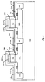
- complimentary CMOS structures comprising silicon substrate 100, isolation elements 102 (composed of SiO 2 ) and complimentary FETs 104a and 104b.
- the structure of complimentary FETs 104a and 104b differ only in that FET 104a comprises n well 106a, p + source 108a and p + drain IIOa, while FET 104b comprises p well 106b, n + source 108b and n + drain 110b.
- the structure of complimentary MOSFETs 104a and 104b is similar.
- both complimentary MOSFETs 104a and 104b comprise (1) gate poly 112 insulated from the well of that MOSFET by a thin layer 114 of SiO 2 , (2) side wall spacers 116 supporting the gate poly 112 of each of MOSFETs 104a and 104b, (3) silicide electrical contacts 117 situated on top of the respective gate poly, source and drain of each of complimentary MOSFETs 104a and 104b, and (4) lightly doped extensions 118 coupling the source and drain of each of complimentary MOSFETs 104a and 104b to the channel region under the gate poly.
- the shallowest junctions are the lightly doped extensions 118, which connect the deep sources and drains to the gate poly channel. Extensions 118 are needed to prevent drain induced barrier lowering (DIBL) and punchthrough.
- DIBL drain induced barrier lowering
- the next step, shown in FIGURE 2, ofboth the fabricating method disclosed in the aforesaid patent and the method of the present invention comprises amorphizing, to the desired uttra-shallow depth of the extensions 118 being fabricated, those regions of the FIGURE 1 MOSFETs being fabricated which include the upper polycrystalline silicon layer 200 of gate poly 112 and the upper crystalline silicon surface layers 202a, 202b, 204a and 204b of welt 106 (which surface layers 202a, 202b, 204a and 204b are to be included in the source and drains 108a, 108b, 110a and 110b of the MOSFETs being fabricated).
- Amorphization may be achieved by ion implantation of a heavy atom, such as argon, silicon or germanium.
- a heavy atom such as argon, silicon or germanium.
- germanium is to be preferred because it is a heavy atom which requires low doses to amorphize silicon, produces abrupt amorphous-crystalline interfaces, and is isoelectronic in the silicon lattice.
- surface layers 202a, 202b, 204a and 204b on the side of gate poly 112, which are to be amorphized extend all the way to an isolation element 102.
- the desired ultra-shallow depth of these layers to be amorphized is substantially 30 nm (which is less than 80 nm)
- a dose of 2 x 10 14 atoms/cm 2 is required to achieve this desired 30 nm amorphization depth.
- a 20 KeV germanium implant at a dose of 2 x 10 14 atoms/cm 2 achieves this desired 30 nm amorphization depth of the layers 202 and 204.
- This implant condition is easily obtainable using existing high current implanters.
- the range of implant dose is between 1 x 10 13 atoms/ cm 2 and 1 x 10 16 atoms/ cm 2
- the range of implant energy is between 5 keV and 400 keV.
- amo rphized layers 202a and 204a have a p + dose of dopant (e.g., boron) ion implanted therein and layers 202b and 204b have an n + dose of dopant (e.g., phosphorous or arsenic) ion implanted therein.
- dopant e.g., boron
- layers 202b and 204b have an n + dose of dopant (e.g., phosphorous or arsenic) ion implanted therein.
- a typical dosage for the lightly-dosed extensions is 5 x 10 14 atoms/cm 2 .
- the implant energies for boron, phosphorous and arsenic typically are, respectively, 250, 2000 and 5000 electron volts. More generally, ion-implant dosages can range between 10 13 to 10 16 atoms/cm 2 and the implant energies can range between 10 and 100,000 electron volts.
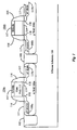
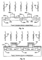
- FIGURE 2a there is shown the melt-threshold-shift heating problem which would occur if the surface of the structure of FIGURE 2 were to be directly irradiated in accordance with the LTA process.
- the FIGURE 2 structure is shown in dashed lines.
- the entire top surface of this structure is flooded by substantially uniform high-power laser radiation 206.
- Applicant has employed a pulsed XeCl excimer laser operating at a wavelength of 308 nm for deriving radiation 206, although another type of excimer laser (e.g., a 193 nm ArF laser, a 248 nm KrF laser or a 351 nm XeF laser) could be used instead.
- a pulsed XeCl excimer laser operating at a wavelength of 308 nm for deriving radiation 206, although another type of excimer laser (e.g., a 193 nm ArF laser, a 248 nm KrF laser or
- isolation elements 102 are composed of SiO 2 which is substantially transparent to incident 308 nm radiation. Depending on the oxide thickness, the normally incident light is selectively absorbed in the silicon underlying the oxide isolation element or is reflected by the isolation element. This is graphically illustrated in Figure 2b which shows the reflectivity of a silicon oxide layer sitting on top of silicon as a function of the oxide layer thickness. Light which is not reflected is absorbed in the underlying silicon. Since the reflectivity of uncoated silicon to incident 308 nm radiation is a constant 0.6, an oxide layer of the wrong thickness can almost double the absorption.
- the solid outline in FIGURE 2a comprises (1) thick outline component 208a representing the relatively large amount of heat energy absorbed in the top surface of the silicon normal to directly incident high-power laser radiation 206, (2) thick outline component 208b representing the relatively large amount of heat energy absorbed in those surfaces of the silicon which are in contact with the bottom of the SiO 2 isolation elements 102 in response to heat energy transferred thereto from the isolation elements of optimal thickness for absorption, and (3) thin outline component 208c representing the relatively negligible amount ofheat energy absorbed in those surfaces of the silicon which are approximately parallel to the incident radiation.
- Applicant's solution to the aforesaid melt-threshold-shift heating problem is to make the surface absorption of radiation uniform by covering the entire top surface of the structure shown in FIGURE 2 with a deposited opaque layer of a material, such as most metals, metal oxides, metal nitrides, metal carbides, carbon, which is highly absorbent of all 308 nm radiation incident thereon and has a melting temperature which is higher than that of silicon.
- the opaque layer of material chosen comprises tantalum nitride because of its low reflectivity, high absorption and compatibility with silicon processing.
- Other desirable materials for the opaque layer are tungsten and tantalum.
- the top surface of SiO 2 isolation elements 102 and the top surface of amorphized silicon 200, 202a, 202b, 204a 204b are first covered with a relatively thin layer 310 (15 nm) of SiO 2 and then this thin layer of SiO 2 is covered with a relatively thick layer 312 (30 nm) of tantalum nitride.
- the thickness of the layer of SiO 2 may range between 5 nm and 50 nm and the thickness of the layer of tantalum nitride is preferably sufficient to absorb all 308 nm radiation incident thereon and may range between 20 nm and 150 nm.
- the thickness of a deposited opaque layer of material should be at least sufficient to result in this material absorbing greater than 50% of all of the of selected-wavelength laser radiation incident thereon.
- the need for the layer of SiO 2 situated between the amorphized silicon and the layer of tantalum nitride arises to prevent the contamination of the silicon which would result if tantalum nitride were in direct contact with the silicon surface.
- amorphous silicon has a factor of 10 lower thermal conductivity, a 300 °C lower melt temperature, and a 30 percent lower reflectivity than crystalline silicon.
- high-power laser radiation 206 incident on the top surface of the highly absorbent tantalum nitride layer 312 is sufficient to heat layer 312 to a relatively high temperature.
- the heat when conducted through the thin SiO 2 layer 310 to the top surface of the amorphized silicon 200, 202a, 202b, 204a 204b, is sufficient to melt the amorphized silicon 200, 202a, 202b, 204a 204b, but is insufficient to melt the crystalline silicon underlying the amorphized silicon, under the areas 202a, 202b, 204a and 204b in FIGURE 3a.
- SiO 2 is a relatively poor conductor of heat and does not absorb the incident radiation directly. Therefore, as indicated in FIGURE 3a by thin solid line 308, the silicon in contact with the sides of isolation elements 102 is only negligibly heated as a result of the high-power laser radiation 206 incident on the top surface of tantalum nitride layer 312.
- the tantalum nitride layer 312 is stripped.
- steps of the fabrication method of the present invention which comprise the LTA process shown in FIGURES 3 and 3a, are employed for forming the ultra-shallow (preferably 30 nm depth) junctions of extensions 118.
- similar steps may be then used to fabricate the deep source and drain regions of the CMOS FET shown in FIGURE 1.
- side wall spacers 116 are fabricated.
- each of the deep source and drain regions located between each side wall spacer 116 and an isolation element 102 is reamorphized to its desired depth deeper than the above-described original amorphization thereof This may be accomplished with higher energy (e.g., 40 KeV) and higher dose (e.g., 6 x 10 14 atoms/cm 2 ) germanium implants. Following such reamorphization, additional dosage of dopants are added to the deep source and drain by ion implantation to preferably provide a total dosage of 1 x 10 15 atoms/cm 2 .
- the implant energies for boron, phosphorous and arsenic remain, respectively, at 250, 2000 and 5000 electron volts, since the final fabricated deep source and deep junction depths are controlled solely by their amphorization depths.
- the amorphization step can be performed before or after the dopant implant step.
- the final steps for fabricating the deep source and deep junction comprise again employing the LTA process, which includes both depositing a tantalum nitride layer that has its top surface exposed to 308 nm radiation that is effective in melting only the amorphized silicon and thereafter stripping the tantalum nitride layer, to thereby form the source and drain junctions to a desired depth determined solely by the depth of the melted silicon of the fabricated CMOS FET. While the desired depth is preferably 120 nm, the range of desired depths is between 80 nm and 200 nm.
- the fabrication of the deep source and drain involve the amorphization of the already-fabricated ultra-shallow (i.e., less than 150 nm depth) junctions, since these already-fabricated ultra-shallow junctions extend all the way to side wall spacers 116.
- the extent of the ultra-shallow junctions may be limited to solely the locations of the extensions and, therefore, not include the locations of the deep source and drain.
- the amorphization for the source and drain locations is independent of the amorphization for the extension locations, so that the amorphization for the source and drain locations may occur either before or after the amorphization for the extension locations.
- the present invention may be employed for fabricating only the extensions of an MOSFET or, alternatively, only the deep source and drain of an MOSFET, rather than both of these.
- the present invention makes the LTA process practical in the fabrication on a selected area of a silicon wafer of a plurality of isolated, spaced, very-shallow-junction MOSFETs.
Landscapes
- Insulated Gate Type Field-Effect Transistor (AREA)
- Recrystallisation Techniques (AREA)
- Metal-Oxide And Bipolar Metal-Oxide Semiconductor Integrated Circuits (AREA)
Applications Claiming Priority (3)
| Application Number | Priority Date | Filing Date | Title |
|---|---|---|---|
| US141842 | 1998-08-27 | ||
| US09/141,842 US5956603A (en) | 1998-08-27 | 1998-08-27 | Gas immersion laser annealing method suitable for use in the fabrication of reduced-dimension integrated circuits |
| PCT/US1998/025264 WO2000013213A1 (en) | 1998-08-27 | 1998-11-25 | Gas immersion laser annealing method suitable for use in the fabrication of reduced-dimension integrated circuits |
Publications (3)
| Publication Number | Publication Date |
|---|---|
| EP1121713A1 EP1121713A1 (en) | 2001-08-08 |
| EP1121713A4 EP1121713A4 (en) | 2003-07-16 |
| EP1121713B1 true EP1121713B1 (en) | 2007-02-07 |
Family
ID=22497510
Family Applications (1)
| Application Number | Title | Priority Date | Filing Date |
|---|---|---|---|
| EP98959621A Expired - Lifetime EP1121713B1 (en) | 1998-08-27 | 1998-11-25 | Gas immersion laser annealing method suitable for use in the fabrication of reduced-dimension integrated circuits |
Country Status (7)
| Country | Link |
|---|---|
| US (1) | US5956603A (https=) |
| EP (1) | EP1121713B1 (https=) |
| JP (1) | JP4295922B2 (https=) |
| KR (1) | KR100582484B1 (https=) |
| DE (1) | DE69837054T2 (https=) |
| TW (1) | TW409293B (https=) |
| WO (1) | WO2000013213A1 (https=) |
Families Citing this family (47)
| Publication number | Priority date | Publication date | Assignee | Title |
|---|---|---|---|---|
| US6521501B1 (en) * | 1999-05-11 | 2003-02-18 | Advanced Micro Devices, Inc. | Method of forming a CMOS transistor having ultra shallow source and drain regions |
| US6586318B1 (en) * | 1999-12-28 | 2003-07-01 | Xerox Corporation | Thin phosphorus nitride film as an N-type doping source used in laser doping technology |
| KR20010085722A (ko) * | 2000-02-29 | 2001-09-07 | 추후제출 | 반도체 물질상에서의 선택적인 레이저 어닐 |
| US6570656B1 (en) | 2000-04-10 | 2003-05-27 | Ultratech Stepper, Inc. | Illumination fluence regulation system and method for use in thermal processing employed in the fabrication of reduced-dimension integrated circuits |
| US6645838B1 (en) * | 2000-04-10 | 2003-11-11 | Ultratech Stepper, Inc. | Selective absorption process for forming an activated doped region in a semiconductor |
| US6635588B1 (en) * | 2000-06-12 | 2003-10-21 | Ultratech Stepper, Inc. | Method for laser thermal processing using thermally induced reflectivity switch |
| JP4389359B2 (ja) * | 2000-06-23 | 2009-12-24 | 日本電気株式会社 | 薄膜トランジスタ及びその製造方法 |
| US6335253B1 (en) | 2000-07-12 | 2002-01-01 | Chartered Semiconductor Manufacturing Ltd. | Method to form MOS transistors with shallow junctions using laser annealing |
| JP2002050764A (ja) * | 2000-08-02 | 2002-02-15 | Matsushita Electric Ind Co Ltd | 薄膜トランジスタ、アレイ基板、液晶表示装置、有機el表示装置およびその製造方法 |
| US6391695B1 (en) * | 2000-08-07 | 2002-05-21 | Advanced Micro Devices, Inc. | Double-gate transistor formed in a thermal process |
| US6635541B1 (en) * | 2000-09-11 | 2003-10-21 | Ultratech Stepper, Inc. | Method for annealing using partial absorber layer exposed to radiant energy and article made with partial absorber layer |
| US6479821B1 (en) * | 2000-09-11 | 2002-11-12 | Ultratech Stepper, Inc. | Thermally induced phase switch for laser thermal processing |
| JP2002184984A (ja) * | 2000-10-26 | 2002-06-28 | Hynix Semiconductor Inc | 半導体素子の製造方法 |
| US6365476B1 (en) | 2000-10-27 | 2002-04-02 | Ultratech Stepper, Inc. | Laser thermal process for fabricating field-effect transistors |
| JP4845299B2 (ja) | 2001-03-09 | 2011-12-28 | 富士通セミコンダクター株式会社 | 半導体装置の製造方法 |
| US6720241B2 (en) * | 2001-06-18 | 2004-04-13 | Matsushita Electric Industrial Co., Ltd. | Method for manufacturing semiconductor device |
| JP4209606B2 (ja) * | 2001-08-17 | 2009-01-14 | 株式会社半導体エネルギー研究所 | 半導体装置の作製方法 |
| TWI282126B (en) * | 2001-08-30 | 2007-06-01 | Semiconductor Energy Lab | Method for manufacturing semiconductor device |
| US7317205B2 (en) * | 2001-09-10 | 2008-01-08 | Semiconductor Energy Laboratory Co., Ltd. | Light emitting device and method of manufacturing a semiconductor device |
| US7112517B2 (en) | 2001-09-10 | 2006-09-26 | Semiconductor Energy Laboratory Co., Ltd. | Laser treatment device, laser treatment method, and semiconductor device fabrication method |
| US6734081B1 (en) * | 2001-10-24 | 2004-05-11 | Lsi Logic Corporation | Shallow trench isolation structure for laser thermal processing |
| US6723634B1 (en) * | 2002-03-14 | 2004-04-20 | Advanced Micro Devices, Inc. | Method of forming interconnects with improved barrier layer adhesion |
| US7135423B2 (en) * | 2002-05-09 | 2006-11-14 | Varian Semiconductor Equipment Associates, Inc | Methods for forming low resistivity, ultrashallow junctions with low damage |
| US6803270B2 (en) * | 2003-02-21 | 2004-10-12 | International Business Machines Corporation | CMOS performance enhancement using localized voids and extended defects |
| JP4589606B2 (ja) | 2003-06-02 | 2010-12-01 | 住友重機械工業株式会社 | 半導体装置の製造方法 |
| JP2005101196A (ja) * | 2003-09-24 | 2005-04-14 | Hitachi Ltd | 半導体集積回路装置の製造方法 |
| US7109087B2 (en) * | 2003-10-03 | 2006-09-19 | Applied Materials, Inc. | Absorber layer for DSA processing |
| US6897118B1 (en) * | 2004-02-11 | 2005-05-24 | Chartered Semiconductor Manufacturing Ltd. | Method of multiple pulse laser annealing to activate ultra-shallow junctions |
| US7145104B2 (en) * | 2004-02-26 | 2006-12-05 | Ultratech, Inc. | Silicon layer for uniformizing temperature during photo-annealing |
| US7622374B2 (en) * | 2005-12-29 | 2009-11-24 | Infineon Technologies Ag | Method of fabricating an integrated circuit |
| KR101323222B1 (ko) * | 2006-03-08 | 2013-10-30 | 어플라이드 머티어리얼스, 인코포레이티드 | 기판상에 형성되는 구조체의 열적 프로세싱을 위한 장치 및 방법 |
| US7569463B2 (en) * | 2006-03-08 | 2009-08-04 | Applied Materials, Inc. | Method of thermal processing structures formed on a substrate |
| US7548364B2 (en) | 2006-07-31 | 2009-06-16 | Applied Materials, Inc. | Ultra-fast beam dithering with surface acoustic wave modulator |
| US20080025354A1 (en) * | 2006-07-31 | 2008-01-31 | Dean Jennings | Ultra-Fast Beam Dithering with Surface Acoustic Wave Modulator |
| US20080045041A1 (en) * | 2006-08-17 | 2008-02-21 | Toshiba America Electronic Components, Inc. | Liquid Immersion Laser Spike Anneal |
| US7759773B2 (en) * | 2007-02-26 | 2010-07-20 | International Business Machines Corporation | Semiconductor wafer structure with balanced reflectance and absorption characteristics for rapid thermal anneal uniformity |
| US7692275B2 (en) * | 2007-02-26 | 2010-04-06 | International Business Machines Corporation | Structure and method for device-specific fill for improved anneal uniformity |
| US7679166B2 (en) * | 2007-02-26 | 2010-03-16 | International Business Machines Corporation | Localized temperature control during rapid thermal anneal |
| US20090096066A1 (en) * | 2007-10-10 | 2009-04-16 | Anderson Brent A | Structure and Method for Device-Specific Fill for Improved Anneal Uniformity |
| US7745909B2 (en) * | 2007-02-26 | 2010-06-29 | International Business Machines Corporation | Localized temperature control during rapid thermal anneal |
| US7732353B2 (en) * | 2007-04-18 | 2010-06-08 | Ultratech, Inc. | Methods of forming a denuded zone in a semiconductor wafer using rapid laser annealing |
| US8148663B2 (en) * | 2007-07-31 | 2012-04-03 | Applied Materials, Inc. | Apparatus and method of improving beam shaping and beam homogenization |
| WO2011066548A1 (en) * | 2009-11-30 | 2011-06-03 | Uvt Tech Systems, Inc. | Laser doping |
| US8021950B1 (en) | 2010-10-26 | 2011-09-20 | International Business Machines Corporation | Semiconductor wafer processing method that allows device regions to be selectively annealed following back end of the line (BEOL) metal wiring layer formation |
| US9302348B2 (en) | 2011-06-07 | 2016-04-05 | Ultratech Inc. | Ultrafast laser annealing with reduced pattern density effects in integrated circuit fabrication |
| US10439720B2 (en) | 2017-05-19 | 2019-10-08 | Adolite Inc. | FPC-based optical interconnect module on glass interposer |
| JP7542350B2 (ja) * | 2020-07-21 | 2024-08-30 | Jswアクティナシステム株式会社 | レーザアニール装置、レーザアニール方法、及び半導体装置の製造方法 |
Family Cites Families (12)
| Publication number | Priority date | Publication date | Assignee | Title |
|---|---|---|---|---|
| JPS5669837A (en) * | 1979-11-12 | 1981-06-11 | Fujitsu Ltd | Manufacture of semiconductor device |
| US4371421A (en) * | 1981-04-16 | 1983-02-01 | Massachusetts Institute Of Technology | Lateral epitaxial growth by seeded solidification |
| JPS5856409A (ja) * | 1981-09-30 | 1983-04-04 | Toshiba Corp | 半導体装置の製造方法 |
| JPS59115574A (ja) * | 1982-12-23 | 1984-07-04 | Semiconductor Energy Lab Co Ltd | 光電変換装置作製方法 |
| EP0178447B1 (en) * | 1984-10-09 | 1993-02-17 | Fujitsu Limited | A manufacturing method of an integrated circuit based on semiconductor-on-insulator technology |
| US4659392A (en) * | 1985-03-21 | 1987-04-21 | Hughes Aircraft Company | Selective area double epitaxial process for fabricating silicon-on-insulator structures for use with MOS devices and integrated circuits |
| JPH0793258B2 (ja) * | 1985-12-04 | 1995-10-09 | 富士通株式会社 | 導電体膜の再結晶化方法 |
| US4753895A (en) * | 1987-02-24 | 1988-06-28 | Hughes Aircraft Company | Method of forming low leakage CMOS device on insulating substrate |
| US5087576A (en) * | 1987-10-26 | 1992-02-11 | North Carolina State University | Implantation and electrical activation of dopants into monocrystalline silicon carbide |
| US5318915A (en) * | 1993-01-25 | 1994-06-07 | North Carolina State University At Raleigh | Method for forming a p-n junction in silicon carbide |
| US5908307A (en) * | 1997-01-31 | 1999-06-01 | Ultratech Stepper, Inc. | Fabrication method for reduced-dimension FET devices |
| US5918915A (en) * | 1997-11-03 | 1999-07-06 | Calteux; Kenneth J. | Sliding door lock |
-
1998
- 1998-08-27 US US09/141,842 patent/US5956603A/en not_active Expired - Lifetime
- 1998-11-25 JP JP2000568107A patent/JP4295922B2/ja not_active Expired - Fee Related
- 1998-11-25 EP EP98959621A patent/EP1121713B1/en not_active Expired - Lifetime
- 1998-11-25 WO PCT/US1998/025264 patent/WO2000013213A1/en not_active Ceased
- 1998-11-25 KR KR1020017000004A patent/KR100582484B1/ko not_active Expired - Fee Related
- 1998-11-25 DE DE69837054T patent/DE69837054T2/de not_active Expired - Lifetime
-
1999
- 1999-02-26 TW TW088102977A patent/TW409293B/zh not_active IP Right Cessation
Also Published As
| Publication number | Publication date |
|---|---|
| JP4295922B2 (ja) | 2009-07-15 |
| EP1121713A1 (en) | 2001-08-08 |
| DE69837054D1 (de) | 2007-03-22 |
| WO2000013213A1 (en) | 2000-03-09 |
| TW409293B (en) | 2000-10-21 |
| US5956603A (en) | 1999-09-21 |
| DE69837054T2 (de) | 2007-06-06 |
| JP2002524846A (ja) | 2002-08-06 |
| EP1121713A4 (en) | 2003-07-16 |
| KR100582484B1 (ko) | 2006-05-24 |
| KR20010074629A (ko) | 2001-08-04 |
Similar Documents
| Publication | Publication Date | Title |
|---|---|---|
| EP1121713B1 (en) | Gas immersion laser annealing method suitable for use in the fabrication of reduced-dimension integrated circuits | |
| EP1012879B1 (en) | Fabrication method for reduced-dimension integrated circuits | |
| US6365476B1 (en) | Laser thermal process for fabricating field-effect transistors | |
| US7091114B2 (en) | Semiconductor device and method of manufacturing the same | |
| US5399506A (en) | Semiconductor fabricating process | |
| JP3277533B2 (ja) | 半導体装置の製造方法 | |
| US20020192914A1 (en) | CMOS device fabrication utilizing selective laser anneal to form raised source/drain areas | |
| US6645838B1 (en) | Selective absorption process for forming an activated doped region in a semiconductor | |
| JP2005502203A (ja) | 半導体ゲートのドーピング方法 | |
| US6555439B1 (en) | Partial recrystallization of source/drain region before laser thermal annealing | |
| US4502205A (en) | Method of manufacturing an MIS type semiconductor device | |
| US20020086502A1 (en) | Method of forming a doped region in a semiconductor material | |
| US4621411A (en) | Laser-enhanced drive in of source and drain diffusions | |
| US6040224A (en) | Method of manufacturing semiconductor devices | |
| JP2002246329A (ja) | 半導体基板の極浅pn接合の形成方法 | |
| JPH0677155A (ja) | 半導体基板の熱処理方法 | |
| JP3031398B2 (ja) | Misトランジスタの作製方法 | |
| JP5103695B2 (ja) | 電界効果型半導体装置の製造方法 | |
| US7351638B1 (en) | Scanning laser thermal annealing | |
| JPH08316487A (ja) | 薄膜半導体装置の製造方法 | |
| WO1997027620A1 (en) | A self-aligned lightly-doped-drain structure for mos transistors | |
| JP2821628B2 (ja) | 半導体装置の製造方法 | |
| JP3387862B2 (ja) | 半導体装置の作製方法 | |
| JP2002151431A (ja) | 半導体基板の極浅pn接合の形成方法 | |
| JP3077804B2 (ja) | 半導体装置の製造方法 |
Legal Events
| Date | Code | Title | Description |
|---|---|---|---|
| PUAI | Public reference made under article 153(3) epc to a published international application that has entered the european phase |
Free format text: ORIGINAL CODE: 0009012 |
|
| 17P | Request for examination filed |
Effective date: 20010123 |
|
| AK | Designated contracting states |
Kind code of ref document: A1 Designated state(s): DE GB NL |
|
| RIN1 | Information on inventor provided before grant (corrected) |
Inventor name: WEINER, KURT Inventor name: TALWAR, SOMIT |
|
| A4 | Supplementary search report drawn up and despatched |
Effective date: 20030604 |
|
| RIC1 | Information provided on ipc code assigned before grant |
Ipc: 7H 01L 21/265 B Ipc: 7H 01L 21/268 B Ipc: 7H 01L 21/20 A |
|
| 17Q | First examination report despatched |
Effective date: 20040130 |
|
| RAP1 | Party data changed (applicant data changed or rights of an application transferred) |
Owner name: ULTRATECH, INC. |
|
| GRAP | Despatch of communication of intention to grant a patent |
Free format text: ORIGINAL CODE: EPIDOSNIGR1 |
|
| GRAS | Grant fee paid |
Free format text: ORIGINAL CODE: EPIDOSNIGR3 |
|
| GRAA | (expected) grant |
Free format text: ORIGINAL CODE: 0009210 |
|
| AK | Designated contracting states |
Kind code of ref document: B1 Designated state(s): DE GB NL |
|
| PG25 | Lapsed in a contracting state [announced via postgrant information from national office to epo] |
Ref country code: NL Free format text: LAPSE BECAUSE OF FAILURE TO SUBMIT A TRANSLATION OF THE DESCRIPTION OR TO PAY THE FEE WITHIN THE PRESCRIBED TIME-LIMIT Effective date: 20070207 |
|
| REG | Reference to a national code |
Ref country code: GB Ref legal event code: FG4D |
|
| REF | Corresponds to: |
Ref document number: 69837054 Country of ref document: DE Date of ref document: 20070322 Kind code of ref document: P |
|
| NLV1 | Nl: lapsed or annulled due to failure to fulfill the requirements of art. 29p and 29m of the patents act | ||
| PLBE | No opposition filed within time limit |
Free format text: ORIGINAL CODE: 0009261 |
|
| STAA | Information on the status of an ep patent application or granted ep patent |
Free format text: STATUS: NO OPPOSITION FILED WITHIN TIME LIMIT |
|
| 26N | No opposition filed |
Effective date: 20071108 |
|
| PGFP | Annual fee paid to national office [announced via postgrant information from national office to epo] |
Ref country code: DE Payment date: 20171121 Year of fee payment: 20 |
|
| PGFP | Annual fee paid to national office [announced via postgrant information from national office to epo] |
Ref country code: GB Payment date: 20171122 Year of fee payment: 20 |
|
| REG | Reference to a national code |
Ref country code: DE Ref legal event code: R071 Ref document number: 69837054 Country of ref document: DE |
|
| REG | Reference to a national code |
Ref country code: GB Ref legal event code: PE20 Expiry date: 20181124 |
|
| PG25 | Lapsed in a contracting state [announced via postgrant information from national office to epo] |
Ref country code: GB Free format text: LAPSE BECAUSE OF EXPIRATION OF PROTECTION Effective date: 20181124 |