EP1115019A2 - Objectif de projection avec des éléments asphériques - Google Patents
Objectif de projection avec des éléments asphériques Download PDFInfo
- Publication number
- EP1115019A2 EP1115019A2 EP00127786A EP00127786A EP1115019A2 EP 1115019 A2 EP1115019 A2 EP 1115019A2 EP 00127786 A EP00127786 A EP 00127786A EP 00127786 A EP00127786 A EP 00127786A EP 1115019 A2 EP1115019 A2 EP 1115019A2
- Authority
- EP
- European Patent Office
- Prior art keywords
- projection exposure
- lens
- lens according
- lenses
- exposure lens
- Prior art date
- Legal status (The legal status is an assumption and is not a legal conclusion. Google has not performed a legal analysis and makes no representation as to the accuracy of the status listed.)
- Withdrawn
Links
- 230000003287 optical effect Effects 0.000 claims abstract description 41
- 239000000463 material Substances 0.000 claims description 16
- WUKWITHWXAAZEY-UHFFFAOYSA-L calcium difluoride Chemical compound [F-].[F-].[Ca+2] WUKWITHWXAAZEY-UHFFFAOYSA-L 0.000 claims description 11
- 229910001634 calcium fluoride Inorganic materials 0.000 claims description 10
- 238000003384 imaging method Methods 0.000 claims description 10
- 230000004075 alteration Effects 0.000 claims description 8
- 238000000034 method Methods 0.000 claims description 7
- VYPSYNLAJGMNEJ-UHFFFAOYSA-N Silicium dioxide Chemical compound O=[Si]=O VYPSYNLAJGMNEJ-UHFFFAOYSA-N 0.000 claims description 6
- 230000005499 meniscus Effects 0.000 claims description 4
- 239000013078 crystal Substances 0.000 claims description 3
- 230000002708 enhancing effect Effects 0.000 claims description 2
- 238000001459 lithography Methods 0.000 claims description 2
- 239000010409 thin film Substances 0.000 claims description 2
- 229910001632 barium fluoride Inorganic materials 0.000 claims 2
- KRHYYFGTRYWZRS-UHFFFAOYSA-M Fluoride anion Chemical compound [F-] KRHYYFGTRYWZRS-UHFFFAOYSA-M 0.000 claims 1
- 239000010453 quartz Substances 0.000 claims 1
- 238000012937 correction Methods 0.000 description 13
- 238000013461 design Methods 0.000 description 9
- 238000005286 illumination Methods 0.000 description 8
- 230000000694 effects Effects 0.000 description 7
- 230000009467 reduction Effects 0.000 description 6
- 238000004519 manufacturing process Methods 0.000 description 5
- 238000010276 construction Methods 0.000 description 4
- 238000010521 absorption reaction Methods 0.000 description 3
- 239000005350 fused silica glass Substances 0.000 description 3
- 238000000206 photolithography Methods 0.000 description 3
- 239000004065 semiconductor Substances 0.000 description 3
- 238000010438 heat treatment Methods 0.000 description 2
- 238000000926 separation method Methods 0.000 description 2
- 241000315040 Omura Species 0.000 description 1
- 230000001133 acceleration Effects 0.000 description 1
- 238000005452 bending Methods 0.000 description 1
- 230000005540 biological transmission Effects 0.000 description 1
- 230000015556 catabolic process Effects 0.000 description 1
- 230000003247 decreasing effect Effects 0.000 description 1
- 238000006731 degradation reaction Methods 0.000 description 1
- 230000001419 dependent effect Effects 0.000 description 1
- 238000011161 development Methods 0.000 description 1
- 238000005516 engineering process Methods 0.000 description 1
- 230000031700 light absorption Effects 0.000 description 1
- 238000001393 microlithography Methods 0.000 description 1
- 238000012986 modification Methods 0.000 description 1
- 230000004048 modification Effects 0.000 description 1
- 239000005304 optical glass Substances 0.000 description 1
- 230000010363 phase shift Effects 0.000 description 1
- 238000007639 printing Methods 0.000 description 1
- 230000008569 process Effects 0.000 description 1
- 210000001747 pupil Anatomy 0.000 description 1
- 238000010926 purge Methods 0.000 description 1
- 230000005855 radiation Effects 0.000 description 1
- 239000007787 solid Substances 0.000 description 1
- 239000000758 substrate Substances 0.000 description 1
- 238000012546 transfer Methods 0.000 description 1
Images


Classifications
-
- G—PHYSICS
- G02—OPTICS
- G02B—OPTICAL ELEMENTS, SYSTEMS OR APPARATUS
- G02B17/00—Systems with reflecting surfaces, with or without refracting elements
- G02B17/08—Catadioptric systems
- G02B17/0892—Catadioptric systems specially adapted for the UV
-
- G—PHYSICS
- G02—OPTICS
- G02B—OPTICAL ELEMENTS, SYSTEMS OR APPARATUS
- G02B13/00—Optical objectives specially designed for the purposes specified below
- G02B13/14—Optical objectives specially designed for the purposes specified below for use with infrared or ultraviolet radiation
- G02B13/143—Optical objectives specially designed for the purposes specified below for use with infrared or ultraviolet radiation for use with ultraviolet radiation
-
- G—PHYSICS
- G02—OPTICS
- G02B—OPTICAL ELEMENTS, SYSTEMS OR APPARATUS
- G02B13/00—Optical objectives specially designed for the purposes specified below
- G02B13/18—Optical objectives specially designed for the purposes specified below with lenses having one or more non-spherical faces, e.g. for reducing geometrical aberration
-
- G—PHYSICS
- G02—OPTICS
- G02B—OPTICAL ELEMENTS, SYSTEMS OR APPARATUS
- G02B13/00—Optical objectives specially designed for the purposes specified below
- G02B13/22—Telecentric objectives or lens systems
-
- G—PHYSICS
- G02—OPTICS
- G02B—OPTICAL ELEMENTS, SYSTEMS OR APPARATUS
- G02B17/00—Systems with reflecting surfaces, with or without refracting elements
- G02B17/08—Catadioptric systems
-
- G—PHYSICS
- G03—PHOTOGRAPHY; CINEMATOGRAPHY; ANALOGOUS TECHNIQUES USING WAVES OTHER THAN OPTICAL WAVES; ELECTROGRAPHY; HOLOGRAPHY
- G03F—PHOTOMECHANICAL PRODUCTION OF TEXTURED OR PATTERNED SURFACES, e.g. FOR PRINTING, FOR PROCESSING OF SEMICONDUCTOR DEVICES; MATERIALS THEREFOR; ORIGINALS THEREFOR; APPARATUS SPECIALLY ADAPTED THEREFOR
- G03F7/00—Photomechanical, e.g. photolithographic, production of textured or patterned surfaces, e.g. printing surfaces; Materials therefor, e.g. comprising photoresists; Apparatus specially adapted therefor
- G03F7/70—Microphotolithographic exposure; Apparatus therefor
- G03F7/70216—Mask projection systems
- G03F7/70225—Optical aspects of catadioptric systems, i.e. comprising reflective and refractive elements
-
- G—PHYSICS
- G03—PHOTOGRAPHY; CINEMATOGRAPHY; ANALOGOUS TECHNIQUES USING WAVES OTHER THAN OPTICAL WAVES; ELECTROGRAPHY; HOLOGRAPHY
- G03F—PHOTOMECHANICAL PRODUCTION OF TEXTURED OR PATTERNED SURFACES, e.g. FOR PRINTING, FOR PROCESSING OF SEMICONDUCTOR DEVICES; MATERIALS THEREFOR; ORIGINALS THEREFOR; APPARATUS SPECIALLY ADAPTED THEREFOR
- G03F7/00—Photomechanical, e.g. photolithographic, production of textured or patterned surfaces, e.g. printing surfaces; Materials therefor, e.g. comprising photoresists; Apparatus specially adapted therefor
- G03F7/70—Microphotolithographic exposure; Apparatus therefor
- G03F7/70216—Mask projection systems
- G03F7/70241—Optical aspects of refractive lens systems, i.e. comprising only refractive elements
Definitions
- the present invention relates to a projection exposure lens in a projection exposure apparatus such as a wafer scanner or a wafer stepper used to manufacture semiconductor elements or other microstructure devices by photolithography and, more particularly, to a catadioptric projection optical lens with an object side catadioptric system and a refractive system for use in such a projection exposure apparatus.
- US 5,691,802 to Takahashi is another example, where a first optical element group having positive refracting power between the first deflecting mirror and the concave mirror is requested. This is to reduce the diameter of the mirror, and therefore this positive lens is located near the first deflecting mirror. All examples show a great number of CaF 2 lenses.
- EP 0 736 789 A to Takahashi is an example, where it is requested that between the first deflecting mirror and the concave mirror three lens groups are arranged, with plus minus plus refractive power, also with the aim of reducing the diameter of the concave mirror. Therefore, the first positive lens is located rather near to the first reflecting mirror. Also many CaF 2 lenses are used for achromatization.
- a catadioptric projection exposure lens comprising lenses or mirrors which are aspheric are known from JP 10-10429 and EP 0 869 383.
- JP 10-10429 the aspheric surface is placed in the vicinity of a reflecting mirror.
- JP 10-10429 comprises an intermediate image.
- EP 0 869 383 a catadioptric system comprising at least two aspheric surfaces is known. For correcting off-axis-aberration one of the aspheric surfaces satisfies the condition h/ ⁇ ⁇ 0.85 and for correcting on-axis-aberration the other of the aspheric surfaces satisfies the condition 0.85 ⁇ h/ ⁇ ⁇ 1.2 whereby h is the height at each lens surface of the light beam that is assumed to be emitted from the intersection of the optical axis and the object plane and passes through the lens surfaces with the maximum numerical aperture NA and ⁇ is the radius of the diaphragm of the aperture stop.
- Subject matter of EP 0 869 383 therefore is to ensure a high image quality by using aspheric surfaces.
- EP 0 869 383 Only as a point amongst others EP 0 869 383 mentions that by using aspheric surfaces the number of lenses in a catadioptric system can be decreased. Furthermore EP 0 869 383 relates only to systems with an intermediate image. As special embodiments EP 0 869 383 shows systems with the first aspheric surface placed near the intermediate image while the second aspheric surface is placed near the concave mirror of the catadioptric system or near the aperture stop.
- WO 99/52004 shows embodiments of catadioptric objectives with few lenses, some of them being aspheric. From WO 99/52004 a system with 16 lenses, at least four of them being aspheric lenses and a numerical aperture of 0.65 is known.
- Said further object is achieved by reducing the number of lenses in the second double passed lens system of the projection exposure lens since in the double passed lens system undesirable effects of absorption in the lens material and of reflection losses at the surface count twice.
- the second lens system comprises at maximum five lenses, preferably two or three lenses.
- negative refraction power is arranged in the second lens system between the optical elements for splitting beam and the concave mirror. Said negative refraction power is split into advantageously two negative lenses.
- the second lens system provides for a over correction while the first and third lens system provides for a under correction.
- the long drift section in the second lens system according to the invention provides for several advantages:
- An advantageous projection exposure apparatus of claim 62 is obtained by incorporating a projection exposure lens according to at least one of claims 1 to 61 into a known apparatus.
- a method of producing microstructured devices by lithography according to the invention is characterized by the use of a projection exposure apparatus according to the preceding claim 62.
- Claim 63 gives an advantageous mode of this method.
- a projection exposure apparatus includes for example an excimer laser light source with an arrangement moderately narrowing bandwidth.
- An illumination system produces a large field, sharply limited and illuminated very homogeneously, which matches the telecentricity requirements of the projection lens, and with an illumination mode to choice.
- Such mode may be conventional illumination of variable degree of coherence, annular or quadrupole illumination.
- a mask or a reticle is displaced in the illuminated area by a mask resp. reticle holding and handling system which includes the scanning drive in case of a wafer scanner projection exposure apparatus. Subsequently follows the projection exposure lens according to the invention to be described in detail subsequently.
- the projection exposure lens produces a reduced scale image of the mask on a wafer.
- the wafer is held, handled and eventually scanned by a scanning unit.
- control unit All systems are controlled by control unit. Such unit and the method of its use is known in the art of microlithographic projection exposure.
- This design concept can be easliy modified for 126 nm wavelength with appropriate lens material, e.g. LiF.
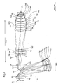
- the example shown in the sectional view of figure 1 has the lens data given in Table 1 in code-V-format in the annex and makes use only of fused silica lenses. As only one lens material is used, this design can easily be adapted for other wavelengths as 248 nm or 157 nm.
- the numbers for the objects in table 1 are identical to the reference signs in figure 1.
- the intermediate image IMI is freely accessible, so that it is easily possible to insert a field stop.
- the aperture stop STO is also well accessible.
- Beam splitting can be achieved e.g. by a physical beam splitter, e.g. a beam splitter prism as disclosed in US 5,742,436. The content of this document is enclosed fully herewith.
- deflecting mirrors An alternative is the usage of deflecting mirrors.
- the deflecting mirrors in the catadioptric system are defined in their geometry by the demands of separation of the light beams to and from the concave mirror 12 and of clearance from the lenses.
- deflection mirrors allow for a straight optical axis and parallel situation of origin plane 0 and image plane IMG, i.e. mask resp. reticle and wafer are parallel and can easily be scanned.
- one of the deflecting mirrors can be abandoned or eventually be replaced by a deflecting mirror in the third lens system TLS which is a refractive lens.
- the deflecting mirrors can be replaced by other deflecting optical elements, e.g. prisms.
- a moderate positive lens comprising surfaces 2, 3 is placed near the origin plane 1 in the first lens system FLS, which is a single beam area. Its focal length is approximately equal to its distance from the concave mirror 13.
- a further positive lens is located as a first lens with surfaces 6, 7 in the second doubly passed lens system SLS consisting of three lenses with surfaces 6, 7, 8, 9, 10, 11.
- SLS doubly passed lens system
- the two negative lenses with surfaces 8, 9, 10, 11 of the second lens system SLS cooperate with the concave mirror 13 in a known manner, giving increased angles of incidence and stronger curvature, thus stronger correcting influence of the concave mirror 13.
- the number of lenses in the doubly passed area of the catadioptric system is restricted to a low number, e.g. three as in this embodiment, since in this part of the optical system every lens counts double with respect to system energy transmission and wavefront quality degradation - without giving more degrees of freedom for correction.
- the embodiment according to figure 1 comprises only one aspheric surface 9, 16 in the double passed second lens system SLS of the projection exposure lens.
- the aspheric surface 9, 16 is situated on the wafer or image IM-side of the lens comprising said surface.
- a field stop is inserted, which reduces stray light favourably.
- the third lens system TLS following the intermediate image IMI is in principle known from the art.
- the third lens system does not comprise any aspheric surface.
- the details of the design are given in table 1 in code V-format in the annex of the application.
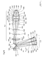
- Figure 2 and table 2 show a design variant.
- the second lens system SLS comprises in total four lenses with surfaces which are passed twice.
- the aspheric surface 160 is situated in the third lens system TLS facing towards the image IMG resp. the wafer.
- the details of this embodiment are given in table 2 in code-V-format in the annex.
- the numbers for the objects in table 2 are identical to the reference signs in figure 2.
- the catadioptric system comprising the second lens system and the concave mirror shows a major revision, since the aspheric surface is situated on the concave mirror 211. This allows for reducing the number of lenses in the catadioptric system to a total number of three. Only the two negative lenses with surfaces 206, 207, 208, 209 have to be passed twice.
- the projection exposure lens comprises only one aspheric surface
- a further aspheric surface is situated in the third lens system TLS.
- the further aspheric surface in the third lens system faces towards the image IMG resp. the wafer.
- a fifth embodiment is given in figure 5 and table 5.
- the aspheric surfaces are situated in the third lens system on surface 533, 539 far away from the intermediate image IMI and in the second lens system SLS.
- the concave mirror 513 of the second lens system comprises an aspheric surface.
- the aspheric surfaces are situated in the third lens system TLS on surface 631, 637, 648 far away from the intermediate image IMI as in embodiment 6 and in the first lens system on surface 603.
- the aspheric surface of the first lens system is situated on a lens near the object 0 resp. reticle instead on the concave mirror.
- table 7 Details are given in table 7 in code-V-format in the annex.
- the number of the object in table 7 corresponds to the reference number in figure 7.
- WO 99/52004 cited in the inductory part of this application shows that with a generic catadioptric objective image side numerical apertures of up to 0.65 can be obtained with less than 16 lenses when entering at least 4 aspherical lenses.
- the invention shows that increased resolution capabilities with numerical apertures of 0.7 to 0.85 and more, at unrestricted image fields and with state of the art correction, are obtained with lesser aspheres in the 0.7 NA range. With the number of 16 lenses and one aspherical surface per lens and on the concave mirror even 0.85 NA is demonstrated as compared to 0.65 NA with 8 aspherical surfaces of 10 lenses and one planar plate of example 4 of the cited WO 99/52004-application.
- At least one lens is inserted, preferably exactly one.
- This lens of the first lens system FLS is also predestined to be used for implementation of correcting surfaces, which may be free-form aspheric surfaces, as it is easily accessible also after complete assembly of the lens.
- this first lens system can be shifted off-axis, with its axis of symmetry arranged between the center of the object field and the optical axis. This allows for a rather symmetric illumination system as conventional with on-axis scanning systems. Generally, in this lens design effort is taken to keep the object side telecentricity very good. So even with the off-axis object field necessitated by the catadioptric design, the illumination system can be rotationally symmetric to the center of the object field, what allows for clearly reduced diameter of this system and consequently great cost reduction.
- the optical axis in the region of this first lens system can be shifted with respect to the parallel optical axis of the refractive partial system, away from the concave mirror. This allows for a better division of the illuminated areas on the two folding mirrors arranged nearby in the preferred variations of the invention.
- the details of the embodiments of Fig. 8 and Fig. 9 are given in table 8 and table 9 in code-V-format in the annex.
- the number of the object in tables 8 and 9 correspond to the reference number in figures 8 and 9.
- a tenth embodiment is shown in figure 10.
- the details of the tenth embodiment are given in table 10 in code-V-format in the annex.
- the number of the object in table 10 corresponds to the reference number in figure 10.
- the tenth embodiment is a 5x reduction system with a magnification ratio of -0.2.
- the projection lens comprises 17 lenses, one concave mirror 1012 and a planar protecting plate 1050/1051. All lenses are made of Calcium Fluoride (CaF 2 ).
- Eight lenses in the third lens system comprise an aspherical surface whereas all lenses in the second lens system and the concave mirror are spherical lenses.
- the rectangular field has the dimensions 22 mm to 7 mm in the image plane IMG, wherein the center of the field is arranged 4.62 mm off axis from the optical axis OA3 of the third lens system TLS.
- the projection lens is optimized for a wavelength of 157.63 nm +/- 0.6 pm.
- the polychromatic wavefront aberration shows a maximum of 10 milliwaves at all field heights
- the monochromatic wavdfroit aberration shows a maximum of 4 milliwaves.
- the folding angle between the optical axis OA2 of the double pass group with the lenses with surfaces 1006, 1007, 1008, 1009, 1010, 1011 and the axis OA1 of the first lens group is 104°. Therefore all light beams at the lenses of the double pass second lens system and the concave mirror 1012 are more distant from the object plane O than the first lens of the first lens group from the object plane is.
- Fig. 11 shows an alternative arrangement of the folding mirrors M1' and M2', where they do not share a common ridge. Here even stronger axis shift is needed. The construction length between object and image can be reduced in this way, and new compromise possibilities in passing by of the light beams at the folding mirrors are opened.
- the folding mirrors of the other shown examples are conveniently established on a common prism substrate.
- the folding mirrors can be internal surfaces of prisms passed by the light beam.
- the higher refractive index of prism material - i.e. calcium fluoride, other crystals, quartz glass or other optical glass - then allows for more compact transfer of high aperture beams.
- they are coated with reflection enhancing thin films, which can even more advantageously correct variations in phase shifts caused by reflections under different angles by adapted thicknesses.
- the folding mirrors can be formed with slight aspheric - non-rotationally symmetric, free-form surface forms for correction of these phase effects as well as other tiny errors of imaging of the system or of production tolerances.
- the preferred configuration of the invention differs from the cited art in that the double pass lens second lens system and concave mirror are arranged along an unfolded optical axis, with two folding mirrors in the region, where the optical axis of this subsystem crosses with those of the first lens group and the refractive partial objective.
- the folding angle between the optical axis of the double pass second lens system and the other axes advantageously deviates from 90° such that at the lenses and the mirror all light beams are more distant from the object plane than the first lens surface of the first lens group is. Consequently, the necessary free access to the object plane needed for scanning does not interfere with the space needed for the mounts of the optical elements.
- a further issue of the invention lies in the design of the double pass lens group having a minimal number of lenses.
- Each degree of freedom for correction of the imaging obtained by an additional lens here has twice the undesirable effects of absorption in the lens material and of reflection losses at the surfaces. Consequently only the lenses needed for putting into effect the concave mirror, for separating the light bundles at the folding mirrors and for keeping the length of the side arm established by the double pass group relatively short are provided.
- the intermediate image IMI directly follows after the folding mirror arranged subsequent to the double path lens group. Though the space between this folding mirror and the intermediate image tends to be narrow, one or other lens can well be introduced here.
- the lenses arranged after and near the intermediate image IMI are illuminated by light bundles situated strongly off axis, so that lens heating caused by light absorption leads to strongly asymmetric disturbing effects. Consequently, the number of lenses in this space is kept low, with normal forms and thicknesses to keep these lens heating influences low.
- the effect of aspherization of the first lens at the object side shows stronger influence onto distortion than a lens very near to the intermediate image can have.
- EP 0 869 383 gives another condition for aspherical surfaces, namely 0.85 ⁇ h/ ⁇ ⁇ 1.2, which is of less relevance, as shown by the example of Fig. 9 and table 9.
- a long drift space intermediate the intermediate image IMI and the aperture stop STO is typical, while the space between aperture stop STO and image plane IMG is densely packed with lenses.
- a meniscus concave versus the aperture stop STO, establishing a positive air lens with the neighboring lens is a typical correcting element introduced in previous applications of the inventors.
- This concave surface (844 in Fig. 9) is also a very effective location of an aspheric surface.
- this or other asphere in the space between aperture stop STO and image plane IMG is paired by an asphere (834 in Fig. 9) arranged approximately symmetrically on the other side of the aperture stop STO.
- the most image-sideward lens is advantageously aspherized, namely on its image side, as surface 849 in Fig. 9 and as surface 749 in Fig. 8.
- the greatest incidence angles of the light rays occur and give special influence of the aspherics here.
- the 16 lenses and 1 concave mirror obtain this at a wavefront error of maximal rms of 21 milliwaves with only 5 aspherical surfaces as described above.
- the object side as well as the image side of such objectives can be a planar surface, either by introducing a planar protecting plate as is in widespread use, e.g. in WO 99/52004, or by changing design under the restriction of a planar face.
Landscapes
- Physics & Mathematics (AREA)
- General Physics & Mathematics (AREA)
- Optics & Photonics (AREA)
- Health & Medical Sciences (AREA)
- Toxicology (AREA)
- Lenses (AREA)
- Exposure And Positioning Against Photoresist Photosensitive Materials (AREA)
- Exposure Of Semiconductors, Excluding Electron Or Ion Beam Exposure (AREA)
Applications Claiming Priority (4)
| Application Number | Priority Date | Filing Date | Title |
|---|---|---|---|
| US17352399P | 1999-12-29 | 1999-12-29 | |
| US173523P | 1999-12-29 | ||
| US22279800P | 2000-08-02 | 2000-08-02 | |
| US222798P | 2000-08-02 |
Publications (2)
| Publication Number | Publication Date |
|---|---|
| EP1115019A2 true EP1115019A2 (fr) | 2001-07-11 |
| EP1115019A3 EP1115019A3 (fr) | 2004-07-28 |
Family
ID=26869245
Family Applications (1)
| Application Number | Title | Priority Date | Filing Date |
|---|---|---|---|
| EP00127786A Withdrawn EP1115019A3 (fr) | 1999-12-29 | 2000-12-19 | Objectif de projection avec des éléments asphériques |
Country Status (5)
| Country | Link |
|---|---|
| US (1) | US6665126B2 (fr) |
| EP (1) | EP1115019A3 (fr) |
| JP (1) | JP2001221950A (fr) |
| KR (1) | KR100876153B1 (fr) |
| TW (1) | TW528880B (fr) |
Cited By (17)
| Publication number | Priority date | Publication date | Assignee | Title |
|---|---|---|---|---|
| WO2003036361A1 (fr) * | 2001-10-19 | 2003-05-01 | Nikon Corporation | Systeme optique de projection et appareil d'exposition possedant ledit systeme |
| US6683710B2 (en) | 2001-06-01 | 2004-01-27 | Optical Research Associates | Correction of birefringence in cubic crystalline optical systems |
| WO2004010164A2 (fr) * | 2002-07-18 | 2004-01-29 | Carl Zeiss Smt Ag | Objectif de projection catadioptrique |
| SG105008A1 (en) * | 2002-07-09 | 2004-07-30 | Asml Holding Nv | Relay lens used in an illumination system of a lithography system |
| US6844972B2 (en) | 2001-10-30 | 2005-01-18 | Mcguire, Jr. James P. | Reducing aberration in optical systems comprising cubic crystalline optical elements |
| WO2005040928A1 (fr) * | 2003-10-15 | 2005-05-06 | Carl Zeiss Smt Ag | Objectif de projection compacte pour lithographie arf |
| EP1544678A1 (fr) * | 2003-12-18 | 2005-06-22 | ASML Netherlands B.V. | Appareil lithographique et méthode de fabrication d'un dispositif |
| US6958864B2 (en) | 2002-08-22 | 2005-10-25 | Asml Netherlands B.V. | Structures and methods for reducing polarization aberration in integrated circuit fabrication systems |
| US6970232B2 (en) | 2001-10-30 | 2005-11-29 | Asml Netherlands B.V. | Structures and methods for reducing aberration in integrated circuit fabrication systems |
| US6995908B2 (en) | 2001-10-30 | 2006-02-07 | Asml Netherlands B.V. | Methods for reducing aberration in optical systems |
| US6995930B2 (en) | 1999-12-29 | 2006-02-07 | Carl Zeiss Smt Ag | Catadioptric projection objective with geometric beam splitting |
| US7453641B2 (en) | 2001-10-30 | 2008-11-18 | Asml Netherlands B.V. | Structures and methods for reducing aberration in optical systems |
| US7551362B2 (en) | 2002-08-23 | 2009-06-23 | Nikon Corporation | Projection optical system and method for photolithography and exposure apparatus and method using same |
| US9081295B2 (en) | 2003-05-06 | 2015-07-14 | Nikon Corporation | Catadioptric projection optical system, exposure apparatus, and exposure method |
| US9500943B2 (en) | 2003-05-06 | 2016-11-22 | Nikon Corporation | Projection optical system, exposure apparatus, and exposure method |
| CN110998447A (zh) * | 2017-04-03 | 2020-04-10 | 卡尔蔡司Smt有限责任公司 | 投射镜头、投射曝光设备和投射曝光方法 |
| CN112269256A (zh) * | 2020-10-21 | 2021-01-26 | 麦克奥迪实业集团有限公司 | 一种显微镜物镜 |
Families Citing this family (34)
| Publication number | Priority date | Publication date | Assignee | Title |
|---|---|---|---|---|
| US6157498A (en) | 1996-06-19 | 2000-12-05 | Nikon Corporation | Dual-imaging optical system |
| US6680803B2 (en) * | 1996-12-21 | 2004-01-20 | Carl-Zeiss Smt Ag | Partial objective in an illuminating systems |
| US7130129B2 (en) | 1996-12-21 | 2006-10-31 | Carl Zeiss Smt Ag | Reticle-masking objective with aspherical lenses |
| EP1293830A1 (fr) * | 1998-06-08 | 2003-03-19 | Nikon Corporation | Méthode et appareil d'exposition par projection |
| JP2002350774A (ja) * | 2001-05-29 | 2002-12-04 | Minolta Co Ltd | 投影光学系とその光学調整方法 |
| US20040218271A1 (en) * | 2001-07-18 | 2004-11-04 | Carl Zeiss Smt Ag | Retardation element made from cubic crystal and an optical system therewith |
| JP4292497B2 (ja) * | 2002-04-17 | 2009-07-08 | 株式会社ニコン | 投影光学系、露光装置および露光方法 |
| US6898025B2 (en) * | 2002-06-04 | 2005-05-24 | Pentax Corporation | Projection aligner and optical system therefor |
| US7869121B2 (en) * | 2003-02-21 | 2011-01-11 | Kla-Tencor Technologies Corporation | Small ultra-high NA catadioptric objective using aspheric surfaces |
| WO2005006026A2 (fr) * | 2003-07-01 | 2005-01-20 | Nikon Corporation | Utilisation de fluides specifies isotopiquement comme elements optiques |
| WO2005033800A1 (fr) * | 2003-09-09 | 2005-04-14 | Carl Zeiss Smt Ag | Objectif de lithographie et installation d'eclairage par projection dotee d'au moins un objectif de lithographie de ce type |
| US8208198B2 (en) | 2004-01-14 | 2012-06-26 | Carl Zeiss Smt Gmbh | Catadioptric projection objective |
| US20080151364A1 (en) | 2004-01-14 | 2008-06-26 | Carl Zeiss Smt Ag | Catadioptric projection objective |
| KR101213831B1 (ko) | 2004-05-17 | 2012-12-24 | 칼 짜이스 에스엠티 게엠베하 | 중간이미지를 갖는 카타디옵트릭 투사 대물렌즈 |
| US7511798B2 (en) * | 2004-07-30 | 2009-03-31 | Asml Holding N.V. | Off-axis catadioptric projection optical system for lithography |
| JP4780412B2 (ja) * | 2004-09-13 | 2011-09-28 | 株式会社ニコン | 投影光学系、投影光学系の製造方法、露光装置及び露光方法 |
| US7184124B2 (en) * | 2004-10-28 | 2007-02-27 | Asml Holding N.V. | Lithographic apparatus having an adjustable projection system and device manufacturing method |
| TWI305107B (en) | 2005-09-29 | 2009-01-01 | Young Optics Inc | Optical projection apparatus |
| WO2007123586A2 (fr) * | 2006-01-19 | 2007-11-01 | The Regents Of The University Of California | Oeil composite biomimétique microfabriqué |
| KR20080106505A (ko) * | 2006-04-03 | 2008-12-08 | 가부시키가이샤 니콘 | 투영 광학계, 노광 장치, 및 디바이스 제조 방법 |
| DE102006022958A1 (de) * | 2006-05-11 | 2007-11-22 | Carl Zeiss Smt Ag | Projektionsbelichtungsanlage, Projektionsbelichtungsverfahren und Verwendung eines Projektionsobjektivs |
| US7929114B2 (en) * | 2007-01-17 | 2011-04-19 | Carl Zeiss Smt Gmbh | Projection optics for microlithography |
| DE102008023765A1 (de) | 2007-05-15 | 2008-11-20 | Carl Zeiss Smt Ag | Verfahren zum Korrigieren von einwelligen Abbildungsfehlern eines Projektionsobjektivs einer mikrolithographischen Projektionsbelichtungsanlage, Projektionsobjektiv einer solchen Belichtungsanlage sowie Herstellungsverfahren für mikrostrukturierte Bauelemente |
| DE102008041144A1 (de) | 2007-08-21 | 2009-03-05 | Carl Zeiss Smt Ag | Optische Anordnung und optisches Abbildungssystem damit, Verfahren zu deren Optimierung und Verfahren zum Herstellen eines optischen Elements |
| US7760425B2 (en) * | 2007-09-05 | 2010-07-20 | Carl Zeiss Smt Ag | Chromatically corrected catadioptric objective and projection exposure apparatus including the same |
| DE102007054731A1 (de) | 2007-11-14 | 2009-05-20 | Carl Zeiss Smt Ag | Optisches Element zur Reflexion von UV-Strahlung, Herstellungsverfahren dafür und Projektionsbelichtungsanlage damit |
| DE102007055567A1 (de) * | 2007-11-20 | 2009-05-28 | Carl Zeiss Smt Ag | Optisches System |
| US8345350B2 (en) | 2008-06-20 | 2013-01-01 | Carl Zeiss Smt Gmbh | Chromatically corrected objective with specifically structured and arranged dioptric optical elements and projection exposure apparatus including the same |
| US20090316256A1 (en) * | 2008-06-20 | 2009-12-24 | Carl Zeiss Smt Ag | Chromatically corrected objective and projection exposure apparatus including the same |
| WO2011116792A1 (fr) | 2010-03-26 | 2011-09-29 | Carl Zeiss Smt Gmbh | Système optique, appareil d'exposition et procédé de correction de front d'onde |
| JP6282742B2 (ja) | 2013-09-09 | 2018-02-21 | カール・ツァイス・エスエムティー・ゲーエムベーハー | マイクロリソグラフィ投影露光装置及びそのような装置における光学波面変形を補正する方法 |
| DE102014204171A1 (de) | 2014-03-06 | 2015-09-24 | Carl Zeiss Smt Gmbh | Optisches Element und optische Anordnung damit |
| DE102015218328B4 (de) | 2015-09-24 | 2019-01-17 | Carl Zeiss Smt Gmbh | Optisches System zur Feldabbildung und/oder Pupillenabbildung |
| DE102016224400A1 (de) * | 2016-12-07 | 2018-06-07 | Carl Zeiss Smt Gmbh | Katadioptrisches Projektionsobjektiv und Verfahren zu seiner Herstellung |
Citations (2)
| Publication number | Priority date | Publication date | Assignee | Title |
|---|---|---|---|---|
| EP0350955A2 (fr) * | 1988-07-15 | 1990-01-17 | Svg Lithography Systems, Inc. | Dispositif optique de réduction |
| WO1999052004A1 (fr) * | 1998-04-07 | 1999-10-14 | Nikon Corporation | Appareil et procede d'exposition a projection, et systeme optique reflechissant a refraction |
Family Cites Families (11)
| Publication number | Priority date | Publication date | Assignee | Title |
|---|---|---|---|---|
| US5220454A (en) * | 1990-03-30 | 1993-06-15 | Nikon Corporation | Cata-dioptric reduction projection optical system |
| JP2847883B2 (ja) * | 1990-03-30 | 1999-01-20 | 株式会社ニコン | 反射屈折縮小投影光学系 |
| USRE36740E (en) * | 1990-03-30 | 2000-06-20 | Nikon Corporation | Cata-dioptric reduction projection optical system |
| JP3085481B2 (ja) * | 1991-09-28 | 2000-09-11 | 株式会社ニコン | 反射屈折縮小投影光学系、及び該光学系を備えた露光装置 |
| JP3635684B2 (ja) * | 1994-08-23 | 2005-04-06 | 株式会社ニコン | 反射屈折縮小投影光学系、反射屈折光学系、並びに投影露光方法及び装置 |
| JPH08203812A (ja) * | 1995-01-30 | 1996-08-09 | Nikon Corp | 反射屈折縮小投影光学系及び露光装置 |
| US5969882A (en) * | 1997-04-01 | 1999-10-19 | Nikon Corporation | Catadioptric optical system |
| JPH10284365A (ja) * | 1997-04-01 | 1998-10-23 | Nikon Corp | 反射屈折光学系 |
| JPH11326767A (ja) * | 1998-05-07 | 1999-11-26 | Nikon Corp | 反射屈折縮小光学系 |
| EP1293830A1 (fr) * | 1998-06-08 | 2003-03-19 | Nikon Corporation | Méthode et appareil d'exposition par projection |
| DE69933973T2 (de) * | 1998-07-29 | 2007-06-28 | Carl Zeiss Smt Ag | Katadioptrisches optisches system und damit ausgestattete belichtungsvorrichtung |
-
2000
- 2000-12-19 EP EP00127786A patent/EP1115019A3/fr not_active Withdrawn
- 2000-12-27 US US09/751,352 patent/US6665126B2/en not_active Expired - Lifetime
- 2000-12-28 JP JP2000402836A patent/JP2001221950A/ja active Pending
- 2000-12-28 KR KR1020000084568A patent/KR100876153B1/ko not_active IP Right Cessation
- 2000-12-29 TW TW089128337A patent/TW528880B/zh not_active IP Right Cessation
Patent Citations (2)
| Publication number | Priority date | Publication date | Assignee | Title |
|---|---|---|---|---|
| EP0350955A2 (fr) * | 1988-07-15 | 1990-01-17 | Svg Lithography Systems, Inc. | Dispositif optique de réduction |
| WO1999052004A1 (fr) * | 1998-04-07 | 1999-10-14 | Nikon Corporation | Appareil et procede d'exposition a projection, et systeme optique reflechissant a refraction |
Cited By (40)
| Publication number | Priority date | Publication date | Assignee | Title |
|---|---|---|---|---|
| US7426082B2 (en) | 1999-12-29 | 2008-09-16 | Carl Zeiss Smt Ag | Catadioptric projection objective with geometric beam splitting |
| US6995930B2 (en) | 1999-12-29 | 2006-02-07 | Carl Zeiss Smt Ag | Catadioptric projection objective with geometric beam splitting |
| US6917458B2 (en) | 2001-06-01 | 2005-07-12 | Asml Netherlands B.V. | Correction of birefringence in cubic crystalline optical systems |
| US6683710B2 (en) | 2001-06-01 | 2004-01-27 | Optical Research Associates | Correction of birefringence in cubic crystalline optical systems |
| US7075696B2 (en) | 2001-06-01 | 2006-07-11 | Asml Netherlands B.V. | Correction of birefringence in cubic crystalline optical systems |
| US7009769B2 (en) | 2001-06-01 | 2006-03-07 | Asml Netherlands B.V. | Correction of birefringence in cubic crystalline optical systems |
| US6885488B2 (en) | 2001-06-01 | 2005-04-26 | Optical Research Associates | Semiconductor device and method for forming the same using cubic crystalline optical system with reduced birefringence |
| US6947192B2 (en) | 2001-06-01 | 2005-09-20 | Asml Netherlands B.V. | Correction of birefringence in cubic crystalline optical systems |
| WO2003036361A1 (fr) * | 2001-10-19 | 2003-05-01 | Nikon Corporation | Systeme optique de projection et appareil d'exposition possedant ledit systeme |
| US7738172B2 (en) | 2001-10-30 | 2010-06-15 | Asml Netherlands B.V. | Structures and methods for reducing aberration in optical systems |
| US7453641B2 (en) | 2001-10-30 | 2008-11-18 | Asml Netherlands B.V. | Structures and methods for reducing aberration in optical systems |
| US6970232B2 (en) | 2001-10-30 | 2005-11-29 | Asml Netherlands B.V. | Structures and methods for reducing aberration in integrated circuit fabrication systems |
| US6995908B2 (en) | 2001-10-30 | 2006-02-07 | Asml Netherlands B.V. | Methods for reducing aberration in optical systems |
| US6844972B2 (en) | 2001-10-30 | 2005-01-18 | Mcguire, Jr. James P. | Reducing aberration in optical systems comprising cubic crystalline optical elements |
| SG105008A1 (en) * | 2002-07-09 | 2004-07-30 | Asml Holding Nv | Relay lens used in an illumination system of a lithography system |
| US7289277B2 (en) | 2002-07-09 | 2007-10-30 | Asml Holding N.V. | Relay lens used in an illumination system of a lithography system |
| WO2004010164A2 (fr) * | 2002-07-18 | 2004-01-29 | Carl Zeiss Smt Ag | Objectif de projection catadioptrique |
| WO2004010164A3 (fr) * | 2002-07-18 | 2004-06-03 | Zeiss Carl Smt Ag | Objectif de projection catadioptrique |
| US7656582B2 (en) | 2002-08-22 | 2010-02-02 | Asml Netherlands B.V. | Methods for reducing polarization aberration in optical systems |
| US7075720B2 (en) | 2002-08-22 | 2006-07-11 | Asml Netherlands B.V. | Structures and methods for reducing polarization aberration in optical systems |
| US7072102B2 (en) | 2002-08-22 | 2006-07-04 | Asml Netherlands B.V. | Methods for reducing polarization aberration in optical systems |
| US7511885B2 (en) | 2002-08-22 | 2009-03-31 | Asml Netherlands B.V. | Methods for reducing polarization aberration in optical systems |
| US6958864B2 (en) | 2002-08-22 | 2005-10-25 | Asml Netherlands B.V. | Structures and methods for reducing polarization aberration in integrated circuit fabrication systems |
| US7551362B2 (en) | 2002-08-23 | 2009-06-23 | Nikon Corporation | Projection optical system and method for photolithography and exposure apparatus and method using same |
| US7688517B2 (en) | 2002-08-23 | 2010-03-30 | Nikon Corporation | Projection optical system and method for photolithography and exposure apparatus and method using same |
| US7609455B2 (en) | 2002-08-23 | 2009-10-27 | Nikon Corporation | Projection optical system and method for photolithography and exposure apparatus and method using same |
| US7619827B2 (en) | 2002-08-23 | 2009-11-17 | Nikon Corporation | Projection optical system and method for photolithography and exposure apparatus and method using same |
| US7701640B2 (en) | 2002-08-23 | 2010-04-20 | Nikon Corporation | Projection optical system and method for photolithography and exposure apparatus and method using same |
| US9086635B2 (en) | 2003-05-06 | 2015-07-21 | Nikon Corporation | Projection optical system, exposure apparatus, and exposure method |
| US9081295B2 (en) | 2003-05-06 | 2015-07-14 | Nikon Corporation | Catadioptric projection optical system, exposure apparatus, and exposure method |
| US9500943B2 (en) | 2003-05-06 | 2016-11-22 | Nikon Corporation | Projection optical system, exposure apparatus, and exposure method |
| US9606443B2 (en) | 2003-05-06 | 2017-03-28 | Nikon Corporation | Reducing immersion projection optical system |
| US9846366B2 (en) | 2003-05-06 | 2017-12-19 | Nikon Corporation | Projection optical system, exposure apparatus, and exposure method |
| US9933705B2 (en) | 2003-05-06 | 2018-04-03 | Nikon Corporation | Reduction projection optical system, exposure apparatus, and exposure method |
| US10156792B2 (en) | 2003-05-06 | 2018-12-18 | Nikon Corporation | Projection optical system, exposure apparatus, and exposure method |
| WO2005040928A1 (fr) * | 2003-10-15 | 2005-05-06 | Carl Zeiss Smt Ag | Objectif de projection compacte pour lithographie arf |
| US7023524B2 (en) | 2003-12-18 | 2006-04-04 | Asml Netherlands B.V. | Lithographic apparatus and device manufacturing method |
| EP1544678A1 (fr) * | 2003-12-18 | 2005-06-22 | ASML Netherlands B.V. | Appareil lithographique et méthode de fabrication d'un dispositif |
| CN110998447A (zh) * | 2017-04-03 | 2020-04-10 | 卡尔蔡司Smt有限责任公司 | 投射镜头、投射曝光设备和投射曝光方法 |
| CN112269256A (zh) * | 2020-10-21 | 2021-01-26 | 麦克奥迪实业集团有限公司 | 一种显微镜物镜 |
Also Published As
| Publication number | Publication date |
|---|---|
| KR20010062830A (ko) | 2001-07-07 |
| EP1115019A3 (fr) | 2004-07-28 |
| US6665126B2 (en) | 2003-12-16 |
| TW528880B (en) | 2003-04-21 |
| US20020039175A1 (en) | 2002-04-04 |
| KR100876153B1 (ko) | 2008-12-29 |
| JP2001221950A (ja) | 2001-08-17 |
Similar Documents
| Publication | Publication Date | Title |
|---|---|---|
| EP1115019A2 (fr) | Objectif de projection avec des éléments asphériques | |
| US7053986B2 (en) | Projection optical system, exposure apparatus, and device manufacturing method | |
| US5999333A (en) | Exposure apparatus having catadioptric projection optical system | |
| EP0736789B1 (fr) | Système catadioptrique et appareil d'exposition lumineuse utilisante ce système | |
| US5515207A (en) | Multiple mirror catadioptric optical system | |
| US6831731B2 (en) | Projection optical system and an exposure apparatus with the projection optical system | |
| EP1751601B1 (fr) | Objectif de projection catadioptrique avec images intermediaires | |
| JP4717974B2 (ja) | 反射屈折光学系及び該光学系を備える投影露光装置 | |
| US5861997A (en) | Catadioptric reduction projection optical system and exposure apparatus having the same | |
| KR100615068B1 (ko) | 반사 굴절 광학 시스템 및 이를 구비하는 노광 장치 | |
| US5071240A (en) | Reflecting optical imaging apparatus using spherical reflectors and producing an intermediate image | |
| EP0770895B1 (fr) | Système de projection optique avec appareil d'exposition | |
| JP2003535356A (ja) | 非球面レンズ表面が隣接して配置されている投影対物レンズ | |
| WO2005096098A2 (fr) | Objectif de projection, appareil d'exposition de projection et reticule reflechissant destines a la microlithographie | |
| US6081382A (en) | Catadioptric reduction projection optical system | |
| US7957069B2 (en) | Projection optical system | |
| US6069749A (en) | Catadioptric reduction optical system | |
| US7268952B2 (en) | Catadioptric projection system, and exposure apparatus having the same | |
| KR20080011301A (ko) | 결상 시스템, 특히 마이크로 리소그래픽 투영 조명 유닛에사용될 수 있는 결상 시스템 | |
| US7283294B2 (en) | Catadioptric projection optical system, exposure apparatus having the same, device fabrication method | |
| WO2007111104A1 (fr) | Systeme optique de projection, appareil d'exposition et procede de fabrication du dispositif. method | |
| JP2006049527A (ja) | 反射屈折型投影光学系及び当該反射屈折型投影光学系を有する露光装置、デバイス製造方法 | |
| JP2005039211A (ja) | 投影光学系、露光装置及びデバイスの製造方法 | |
| JP2005107362A (ja) | 投影光学系及び露光装置、デバイスの製造方法 |
Legal Events
| Date | Code | Title | Description |
|---|---|---|---|
| PUAI | Public reference made under article 153(3) epc to a published international application that has entered the european phase |
Free format text: ORIGINAL CODE: 0009012 |
|
| AK | Designated contracting states |
Kind code of ref document: A2 Designated state(s): AT BE CH CY DE DK ES FI FR GB GR IE IT LI LU MC NL PT SE TR |
|
| AX | Request for extension of the european patent |
Free format text: AL;LT;LV;MK;RO;SI |
|
| RIC1 | Information provided on ipc code assigned before grant |
Ipc: 7G 02B 17/08 B Ipc: 7G 03F 7/20 B Ipc: 7G 02B 13/18 A |
|
| PUAL | Search report despatched |
Free format text: ORIGINAL CODE: 0009013 |
|
| AK | Designated contracting states |
Kind code of ref document: A3 Designated state(s): AT BE CH CY DE DK ES FI FR GB GR IE IT LI LU MC NL PT SE TR |
|
| AX | Request for extension of the european patent |
Extension state: AL LT LV MK RO SI |
|
| RAP1 | Party data changed (applicant data changed or rights of an application transferred) |
Owner name: CARL-ZEISS-STIFTUNG TRADING AS CARL ZEISS Owner name: CARL ZEISS |
|
| RAP1 | Party data changed (applicant data changed or rights of an application transferred) |
Owner name: CARL ZEISS SMT AG |
|
| 17P | Request for examination filed |
Effective date: 20040713 |
|
| AKX | Designation fees paid |
Designated state(s): DE FR GB NL |
|
| 17Q | First examination report despatched |
Effective date: 20050504 |
|
| 17Q | First examination report despatched |
Effective date: 20050504 |
|
| RAP1 | Party data changed (applicant data changed or rights of an application transferred) |
Owner name: CARL ZEISS SMT AG |
|
| GRAP | Despatch of communication of intention to grant a patent |
Free format text: ORIGINAL CODE: EPIDOSNIGR1 |
|
| STAA | Information on the status of an ep patent application or granted ep patent |
Free format text: STATUS: THE APPLICATION IS DEEMED TO BE WITHDRAWN |
|
| 18D | Application deemed to be withdrawn |
Effective date: 20081016 |