EP1107318B1 - Halbleiterphotodetektor - Google Patents
Halbleiterphotodetektor Download PDFInfo
- Publication number
- EP1107318B1 EP1107318B1 EP00126990A EP00126990A EP1107318B1 EP 1107318 B1 EP1107318 B1 EP 1107318B1 EP 00126990 A EP00126990 A EP 00126990A EP 00126990 A EP00126990 A EP 00126990A EP 1107318 B1 EP1107318 B1 EP 1107318B1
- Authority
- EP
- European Patent Office
- Prior art keywords
- layer
- inp
- optical absorption
- ingaas
- ingaasp
- Prior art date
- Legal status (The legal status is an assumption and is not a legal conclusion. Google has not performed a legal analysis and makes no representation as to the accuracy of the status listed.)
- Expired - Lifetime
Links
- 239000004065 semiconductor Substances 0.000 title claims description 51
- 230000003287 optical effect Effects 0.000 claims description 95
- 238000010521 absorption reaction Methods 0.000 claims description 72
- 229910000530 Gallium indium arsenide Inorganic materials 0.000 claims description 64
- 238000005253 cladding Methods 0.000 claims description 47
- 239000000758 substrate Substances 0.000 claims description 12
- 239000012535 impurity Substances 0.000 description 25
- 230000004044 response Effects 0.000 description 13
- 239000013307 optical fiber Substances 0.000 description 9
- 239000004642 Polyimide Substances 0.000 description 7
- 230000008878 coupling Effects 0.000 description 7
- 238000010168 coupling process Methods 0.000 description 7
- 238000005859 coupling reaction Methods 0.000 description 7
- 229920001721 polyimide Polymers 0.000 description 7
- 229910004205 SiNX Inorganic materials 0.000 description 3
- 230000001747 exhibiting effect Effects 0.000 description 3
- 238000002161 passivation Methods 0.000 description 3
- 230000009467 reduction Effects 0.000 description 3
- 230000004048 modification Effects 0.000 description 2
- 238000012986 modification Methods 0.000 description 2
- 230000001419 dependent effect Effects 0.000 description 1
- 238000011161 development Methods 0.000 description 1
- 230000018109 developmental process Effects 0.000 description 1
- 238000003475 lamination Methods 0.000 description 1
Images


Classifications
-
- B—PERFORMING OPERATIONS; TRANSPORTING
- B82—NANOTECHNOLOGY
- B82Y—SPECIFIC USES OR APPLICATIONS OF NANOSTRUCTURES; MEASUREMENT OR ANALYSIS OF NANOSTRUCTURES; MANUFACTURE OR TREATMENT OF NANOSTRUCTURES
- B82Y20/00—Nanooptics, e.g. quantum optics or photonic crystals
-
- H—ELECTRICITY
- H10—SEMICONDUCTOR DEVICES; ELECTRIC SOLID-STATE DEVICES NOT OTHERWISE PROVIDED FOR
- H10F—INORGANIC SEMICONDUCTOR DEVICES SENSITIVE TO INFRARED RADIATION, LIGHT, ELECTROMAGNETIC RADIATION OF SHORTER WAVELENGTH OR CORPUSCULAR RADIATION
- H10F30/00—Individual radiation-sensitive semiconductor devices in which radiation controls the flow of current through the devices, e.g. photodetectors
- H10F30/20—Individual radiation-sensitive semiconductor devices in which radiation controls the flow of current through the devices, e.g. photodetectors the devices having potential barriers, e.g. phototransistors
- H10F30/21—Individual radiation-sensitive semiconductor devices in which radiation controls the flow of current through the devices, e.g. photodetectors the devices having potential barriers, e.g. phototransistors the devices being sensitive to infrared, visible or ultraviolet radiation
- H10F30/22—Individual radiation-sensitive semiconductor devices in which radiation controls the flow of current through the devices, e.g. photodetectors the devices having potential barriers, e.g. phototransistors the devices being sensitive to infrared, visible or ultraviolet radiation the devices having only one potential barrier, e.g. photodiodes
- H10F30/221—Individual radiation-sensitive semiconductor devices in which radiation controls the flow of current through the devices, e.g. photodetectors the devices having potential barriers, e.g. phototransistors the devices being sensitive to infrared, visible or ultraviolet radiation the devices having only one potential barrier, e.g. photodiodes the potential barrier being a PN homojunction
- H10F30/2215—Individual radiation-sensitive semiconductor devices in which radiation controls the flow of current through the devices, e.g. photodetectors the devices having potential barriers, e.g. phototransistors the devices being sensitive to infrared, visible or ultraviolet radiation the devices having only one potential barrier, e.g. photodiodes the potential barrier being a PN homojunction the devices comprising active layers made of only Group III-V materials
-
- H—ELECTRICITY
- H10—SEMICONDUCTOR DEVICES; ELECTRIC SOLID-STATE DEVICES NOT OTHERWISE PROVIDED FOR
- H10F—INORGANIC SEMICONDUCTOR DEVICES SENSITIVE TO INFRARED RADIATION, LIGHT, ELECTROMAGNETIC RADIATION OF SHORTER WAVELENGTH OR CORPUSCULAR RADIATION
- H10F77/00—Constructional details of devices covered by this subclass
- H10F77/10—Semiconductor bodies
- H10F77/14—Shape of semiconductor bodies; Shapes, relative sizes or dispositions of semiconductor regions within semiconductor bodies
- H10F77/146—Superlattices; Multiple quantum well structures
-
- H—ELECTRICITY
- H10—SEMICONDUCTOR DEVICES; ELECTRIC SOLID-STATE DEVICES NOT OTHERWISE PROVIDED FOR
- H10F—INORGANIC SEMICONDUCTOR DEVICES SENSITIVE TO INFRARED RADIATION, LIGHT, ELECTROMAGNETIC RADIATION OF SHORTER WAVELENGTH OR CORPUSCULAR RADIATION
- H10F77/00—Constructional details of devices covered by this subclass
- H10F77/40—Optical elements or arrangements
- H10F77/413—Optical elements or arrangements directly associated or integrated with the devices, e.g. back reflectors
Definitions
- the present invention relates to a semiconductor photodetector, and more particularly to a semiconductor photodetector exhibiting a high speed response and having a high external quantum efficiency.
- FIG. 1 is a fragmentary cross sectional elevation view illustrative of a conventional semiconductor photodetector.
- the conventional semiconductor photodetector is provided over a semi-insulating InP substrate 20.
- An n+-InGaAsP layer 21 having a thickness of 0.2 micrometers is selectively formed on a first region of an upper surface of the semi-insulating InP substrate 20.
- a first polyimide insulating layer 27a is also selectively formed on a second region of the upper surface of the semi-insulating InP substrate 20.
- a second polyimide insulating layer 27b is selectively formed on a first region of an upper surface of the n+-InGaAsP layer 21.
- the second polyimide insulating layer 27b has a window through which the upper surface of the n+-InGaAsP layer 21 is shown.
- An n-contact 28 of AuGaNi is formed in the window and on the upper surface of the n+-InGaAsP layer 21, so that the n-contact 28 is surrounded by the second polyimide insulating layer 27b.
- a multi-layered structure is provided selectively provided on a second region of the upper surface of the n+-InGaAsP layer 21, so that the multi-layered structure is surrounded by the first and second polyimide insulating layers 27a and 27b.
- the multi-layered structure comprises the following five layers 22, 23, 24, 25 and 26.
- An undoped InGaAs optical absorption layer 22 having a thickness of 0.4 micrometers is selectively provided on the second region of the upper surface of the n+-InGaAsP layer 21.
- a p+-InGaAs optical absorption layer 23 having a thickness of 0.2 micrometers is laminated on the undoped InGaAs optical absorption layer 22.
- a p+-InGaAsP layer 24 having a thickness of 0.2 micrometers is laminated on the p+-InGaAs optical absorption layer 23.
- a p+-InP layer 25 having a thickness of 0.5 micrometers is laminated on the p+-InGaAsP layer 24.
- a p+-InGaAsP layer 26 having a thickness of 0.2 micrometers is laminated on the p+-InP layer 25.
- An upper surface of the p+-InGaAsP layer 26 is leveled to the top surfaces of the first and second polyimide insulating layers 27a and 27b to form a palatalized surface.
- a p-contact 29 of AuZnNi is provided on the palatalized surface, wherein the p-contact 29 is in contact with the p+-InGaAsP layer 26.
- the n-contact 28 and the p-contact 29 are electrically connected to each other through the n+-InGaAsP layer 21, the undoped InGaAs optical absorption layer 22, the p+-InGaAs optical absorption layer 23, the p+-InGaAsP layer 24, the p+-InP layer 25 and the p+-InGaAsP layer 26.
- the optical waveguide comprises the the n+-InGaAsP layer 21, the undoped InGaAs optical absorption layer 22, the p+-InGaAs optical absorption layer 23, the p+-InGaAsP layer 24, the p+-InP layer 25 and the p+-InGaAsP layer 26.
- the n-contact 28 is bonded through a bonding wire to a pad formed on the top surface of the second polyimide insulating film 27b.
- the above undoped InGaAs optical absorption layer 22 further comprises three lamination layers of a p - -InGaAs layer, an i-InGaAs and a p - -InGaAs layer.
- a total thickness of the undoped InGaAs optical absorption layer 22 and the p+-InGaAs optical absorption layer 23 is thin, for example, 0.6 micrometers which is less than 1 micrometer.
- the reduction in the total thickness of the undoped InGaAS optical absorption layer 22 and the p+-InGaAs optical absorption layer 23 shortens a carrier traveling time to improve the high speed response of the conventional semiconductor photodetector.
- An optical absorption region of the above conventional semiconductor photodetector comprises the n+-InGaAsP layer 21, the undoped InGaAs optical absorption layer 22, the p+-InGaAs optical absorption layer 23 and the p+-InGaAsP layer 24.
- a total thickness of the the n+-InGaAsP layer 21, the undoped InGaAs optical absorption layer 22, the p+-InGaAs optical absorption layer 23 and the p+-InGaAsP layer 24 is 1 micrometer.
- the thickness of the optical absorption region of the above conventional semiconductor photodetector is 1 micrometer.
- a spot size of the incident light from the optical fiber is, however, about 9 micrometers. Namely, the thickness of the optical absorption region of the above conventional semiconductor photodetector is much smaller than the spot size of the incident light from the optical fiber, for which reason an external quantum efficiency is low.
- EP 0 889 529 A1 describes a semiconductor light-receiving device having a semiconductor substrate and a multi-layered structure formed on the semiconductor substrate wherein the multi-layered structure has at least one portion which is inclined to a direction of incident light.
- the multi-layered structure comprises buffer layers of InP, clad layers of InGaAsP and a light absorbing layer of InGaAs.
- the present invention provides an optical waveguide structure comprising plural periods of a multi-layered structure which comprises an InGaAs optical absorption layer of a first conductivity type, a pair of first and second InGaAsP cladding layers of the first conductivity type sandwiching the InGaAs optical absorption layer, and a pair of a first InP layer of the first conductivity type and a second InP layer of a second conductivity type, and the first and second InP layers sandwiching the first and second InGaAsP cladding layers.
- the InGaAs optical absorption layer is thin.
- the InGaAs optical absorption layer has a low impurity concentration. This means that a carrier traveling distance through the low impurity semiconductor region is short.
- the first and second InP layers sandwich the first and second InGaAsP cladding layers which further sandwich the thin InGaAs optical absorption layer.
- This sandwich structure allows that application of a low voltage, for example, not higher than 1 volt causes a space charge region in the InGaAs optical absorption layer.
- the above two characteristics allow the semiconductor photodetector having the above novel structure to exhibit the high speed response.
- first and second InP layers sandwich the first and second InGaAsP cladding layers which further sandwich the thin InGaAs optical absorption layer.
- This sandwich structure enlarges an effective area or an effective thickness of the absorption region of the optical waveguide structure even the carrier traveling distance through the low impurity semiconductor region is short.
- the paired first and second InGaAsP cladding layers have the same conductivity type. This improves the coupling efficiency to the incident light from the optical fiber.
- the optical waveguide structure has at least a facet coated with an n-InP layer.
- the n-InP layer protects the p-n junction structure of the above multi-layered structure to ensure a high reliability and a stable dark current characteristic of the semiconductor photodetector.
- the InGaAs optical absorption layer has a thickness in the range of 0.15 micrometers to 0.25 micrometers.
- the InGaAs optical absorption layer is thin.
- the InGaAs optical absorption layer has a low impurity concentration. This means that a carrier traveling distance through the low impurity semiconductor region is short.
- the first and second InP layers sandwich the first and second InGaAsP cladding layers which further sandwich the thin InGaAs optical absorption layer. This sandwich structure allows that application of a low voltage, for example, not higher than 1 volt causes a space charge region in the InGaAs optical absorption layer.
- the above two characteristics allow the semiconductor photodetector having the above novel structure to exhibit the high speed response.
- the plural periods of the multi-layered structure is in the range of 5-20.
- This structure enlarges an effective area or an effective thickness of the absorption region of the optical waveguide structure even the carrier traveling distance through the low impurity semiconductor region is short.
- the paired first and second InGaAsP cladding layers have the same conductivity type. This improves the coupling efficiency to the incident light from the optical fiber.
- each of the first and second InP layers is common to adjacent two of the multi-layered structure.
- the optical waveguide structure includes a sequential laminated structure of an n+-InP layer, an n+-InGaAsP cladding layer, an n--InGaAs optical absorption layer, an n+-InGaAsP cladding layer, a p+-InP layer, an n+-InGaAsP cladding layer, an n - -InGaAS optical absorption layer, and an n+-InGaAsP cladding layer.
- the novel semiconductor photodetector exhibits a high speed response at about 20GHz and having a high external quantum efficiency of not less than 90%.
- the novel semiconductor photodetector is also operable at a low voltage of not more than 1 volt and having a high reliability and a stable dark current characteristic.
- the second present invention provides a semiconductor photodetector comprising : a pair of a p-electrode and an n-electrode ; a substrate ; and an optical waveguide structure electrically connected between the p-electrode and the n-electrode and provided over the substrate, wherein the optical waveguide structure comprises plural periods of a multi-layered structure which comprises an InGaAs optical absorption layer of a first conductivity type, a pair of first and second InGaAsP cladding layers of the first conductivity type sandwiching the InGaAs optical absorption layer, and a pair of a first InP layer of the first conductivity type and a second InP layer of a second conductivity type, and the first and second InP layers sandwiching the first and second InGaAsP cladding layers.
- the InGaAs optical absorption layer is thin.
- the InGaAs optical absorption layer has a low impurity concentration. This means that a carrier traveling distance through the low impurity semiconductor region is short.
- the first and second InP layers sandwich the first and second InGaAsP cladding layers which further sandwich the thin InGaAs optical absorption layer.
- This sandwich structure allows that application of a low voltage, for example, not higher than 1 volt causes a space charge region in the InGaAs optical absorption layer.
- the above two characteristics allow the semiconductor photodetector having the above novel structure to exhibit the high speed response.
- first and second InP layers sandwich the first and second InGaAsP cladding layers which further sandwich the thin InGaAs optical absorption layer.
- This sandwich structure enlarges an effective area or an effective thickness of the absorption region of the optical waveguide structure even the carrier traveling distance through the low impurity semiconductor region is short.
- the paired first and second InGaAsP cladding layers have the same conductivity type. This improves the coupling efficiency to the incident light from the optical fiber.
- the optical waveguide structure has at least a facet coated with an n-InP layer.
- the n-InP layer protects the p-n junction structure of the above multi-layered structure to ensure a high reliability and a stable dark current characteristic of the semiconductor photodetector.
- the InGaAs optical absorption layer has a thickness in the range of 0.15 micrometers to 0.25 micrometers.
- the InGaAs optical absorption layer is thin.
- the InGaAs optical absorption layer has a low impurity concentration. This means that a carrier traveling distance through the low impurity semiconductor region is short.
- the first and second InP layers sandwich the first and second InGaAsP cladding layers which further sandwich the thin InGaAs optical absorption layer. This sandwich structure allows that application of a low voltage, for example, not higher than 1 volt causes a space charge region in the InGaAs optical absorption layer.
- the above two characteristics allow the semiconductor photodetector having the above novel structure to exhibit the high speed response.
- the plural periods of the multi-layered structure is in the range of 5-20.
- This structure enlarges an effective area or an effective thickness of the absorption region of the optical waveguide structure even the carrier traveling distance through the low impurity semiconductor region is short.
- the paired first and second InGaAsP cladding layers have the same conductivity type. This improves the coupling efficiency to the incident light from the optical fiber.
- each of the first and second InP layers is common to adjacent two of the multi-layered structure.
- the optical waveguide structure includes a sequential laminated structure of an n+-InP layer, an n+-InGaAsP cladding layer, an n--InGaAs optical absorption layer, an n+-InGaAsP cladding layer, a p+-InP layer, an n+-InGaAsP cladding layer, an n - -InGaAs optical absorption layer, and an n+-InGaAsP cladding layer.
- the novel semiconductor photodetector exhibits a high speed response at about 20GHz and having a high external quantum efficiency of not less than 90%.
- the novel semiconductor photodetector is also operable at a low voltage of not more than 1 volt and having a high reliability and a stable dark current characteristic.
- FIG. 2A is a schematic perspective view illustrative of a novel semiconductor photodetector in a first embodiment in accordance with the present invention.
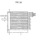
- FIG. 2B is a cross sectional elevation view illustrative of a novel semiconductor photodetector shown in FIG. 2A in a first embodiment in accordance with the present invention.
- the novel semiconductor photodetector is provided over a semi-insulating InP substrate 7.
- An optical waveguide structure is provided over the semi-insulating InP substrate 7.
- the optical waveguide structure comprises five periods of the following multi-layered structure.
- An n+-InP layer 5 is provided on the semi-insulating InP substrate 7, wherein the n+-InP layer 5 has an impurity concentration of 1E16 /cm 3 and a thickness of 0.1 micrometer.
- An n+-InGaAsP cladding layer 3 is provided on the n+-InP layer 5, wherein the n+-InGaAsP cladding layer 3 has an impurity concentration of 1E16 /cm 3 and a thickness of 0.03 micrometer.
- An n--InGaAs optical absorption layer 1 is provided on the n+-InGaAsP cladding layer 3, wherein the n - -InGaAs optical absorption layer 1 has an impurity concentration of 1E15 /cm 3 and a thickness of 0.2 micrometer.
- An n+-InGaAsP cladding layer 2 is provided on the n--InGaAs optical absorption layer 1, wherein the n+-InGaAsP cladding layer 2 has an impurity concentration of 1E16 /cm 3 and a thickness of 0.03 micrometer.
- a p+-InP layer 4 is provided on the n+-InGaAsP cladding layer 2, wherein the p+-InP layer 4 has an impurity concentration of 1E16 /cm 3 and a thickness of 0.1 micrometer.
- the n+-InGaAsP cladding layer 3 is provided on the p+-InP layer 4, wherein the n+-InGaAsP cladding layer 3 has an impurity concentration of 1E16 /cm 3 and a thickness of 0.03 micrometer.
- the n - -InGaAs optical absorption layer 1 is provided on the n+-InGaAsP cladding layer 3, wherein the n - -InGaAS optical absorption layer 1 has an impurity concentration of 1E15 /cm 3 and a thickness of 0.2 micrometer.
- the n+-InGaAsP cladding layer 2 is provided on the n - -InGaAs optical absorption layer 1, wherein the n+-InGaAsP cladding layer 2 has an impurity concentration of 1E16 /cm 3 and a thickness of 0.03 micrometer.
- An n+-InP layer 6 is provided on a facet of the optical waveguide structure, wherein the n+-InP layer 6 has an impurity concentration of 1E16 /cm 3 and a thickness of 0.1 micrometer.
- An SiNx passivation layer 8 is provided which extends on the n+-InP layer 6 and the surface of the optical waveguide structure.
- the SiNx passivation layer 8 has a first opening, in which a p-electrode 9 is provided which is in contact with the p+-InP layer 4.
- the SiNx passivation layer 8 also has a second opening, in which an n-electrode 10 is provided which is in contact with the n+-InP layer 5.
- the n - -InGaAs optical absorption layer 1 is thin.
- the n - -InGaAs optical absorption layer 1 has a low impurity concentration. This means that a carrier traveling distance through the low impurity semiconductor region is short.
- the p+-InP layer 4 and the n+-InP layer 5 sandwich the n+-InGaAsP cladding layer 2 and the n+-InGaAsP cladding layer 3 which further sandwich the thin n--InGaAs optical absorption layer 1.
- This sandwich structure allows that application of a low voltage, for example, not higher than 1 volt causes a space charge region in the n--InGaAs optical absorption layer 1.
- the above two characteristics allow the semiconductor photodetector having the above novel structure to exhibit the high speed response.
- the p+-InP layer 4 and the n+-InP layer 5 sandwich the n+-InGaAsP cladding layer 2 and the n+-InGaAsP cladding layer 3 which further sandwich the thin n--InGaAs optical absorption layer 1.
- This sandwich structure enlarges an effective area or an effective thickness of the absorption region of the optical waveguide structure even the carrier traveling distance through the low impurity semiconductor region is short.
- the n+-InGaAsP cladding layer 2 and the n+-InGaAsP cladding layer 3 have the same conductivity type. This improves the coupling efficiency to the incident light from the optical fiber.
- the n+-InP layer 6 protects the p-n junction structure of the above multi-layered structure to ensure a high reliability and a stable dark current characteristic of the semiconductor photodetector.
- the optical waveguide structure comprises the five periods of the multi-layered structure. This structure enlarges an effective area or an effective thickness of the absorption region of the optical waveguide structure even the carrier traveling distance through the low impurity semiconductor region is short. Further, the n+-InGaAsP cladding layer 2 and the n+-InGaAsP cladding layer 3 have the same conductivity type. This improves the coupling efficiency to the incident light from the optical fiber.
- the novel semiconductor photodetector exhibits a high speed response at about 20GHz and having a high external quantum efficiency of not less than 90%.
- the novel semiconductor photodetector is also operable at a low voltage of not more than 1 volt and having a high reliability and a stable dark current characteristic.
Landscapes
- Chemical & Material Sciences (AREA)
- Engineering & Computer Science (AREA)
- Nanotechnology (AREA)
- Physics & Mathematics (AREA)
- Life Sciences & Earth Sciences (AREA)
- Biophysics (AREA)
- Optics & Photonics (AREA)
- Crystallography & Structural Chemistry (AREA)
- Light Receiving Elements (AREA)
Claims (7)
- Optische Wellenleiterstruktur mit einer Anzahl von Perioden einer Mehrschichtstruktur mit einer optischen InGaAs-Absorptionsschicht (1) eines ersten Leitfähigkeitstyps, einem Paar aus einer ersten und einer zweiten InGaAsP-Deckschicht (2, 3) des ersten Leitfähigkeitstyps, die die optische InGaAs-Absorptionsschicht (1) zwischen sich aufnehmen, und einem Paar aus einer ersten InP-Schicht (5) des ersten Leitfähigkeitstyps und einer zweiten InP-Schicht (4) eines zweiten Leitfähigkeitstyps, wobei die erste und die zweite InP-Schichten (5, 4) die erste und die zweite InGaAsP-Deckschichten (2, 3) zwischen sich aufnehmen, wobei die Richtung von einfallendem Licht parallel zu den Ebenen der Schichten der Mehrschichtstruktur ist.
- Optische Wellenleiterstruktur nach Anspruch 1,
dadurch gekennzeichnet, dass die optische Wellenleiterstruktur zumindest eine Facette aufweist, die mit einer n-InP-Schicht (6) beschichtet ist. - Optische Wellenleiterstruktur nach Anspruch 1,
dadurch gekennzeichnet, dass die optische InGaAs-Absorptionsschicht (1) eine Dicke im Bereich von 0,15 Mikrometern bis 0,25 Mikrometern aufweist. - Optische Wellenleiterstruktur nach Anspruch 1,
dadurch gekennzeichnet, dass die mehreren Perioden der Mehrschichtstruktur im Bereich von 5 bis 20 liegen. - Optische Wellenleiterstruktur nach Anspruch 1,
dadurch gekennzeichnet, dass jede der ersten und zweiten InP-Schichten (5, 4) angrenzenden zwei der Mehrschichtstrukturen gemeinsam ist. - Optische Wellenleiterstruktur nach Anspruch 5,
dadurch gekennzeichnet, dass die optische Wellenleiterstruktur eine sequentiell laminierte Struktur aus einer n+ -InP-Schicht, einer n+ -InGaAsP-Deckschicht, einer optischen n- -InGaAs-Absorptionsschicht, einer n+ -InGaAsP-Deckschicht, einer p+ -InP-Schicht, einer n+ -InGaAsP-Deckschicht, einer optischen n- -InGaAs-Absorptionsschicht und einer n+ -InGaAsP-Deckschicht ist. - Halbleiterphotodetektor mit:einem Paar aus einer p-Elektrode und einer n-Elektrode,einem Substrat undeiner optischen Wellenleiterstruktur nach einem der Ansprüche 1 bis 6, die elektrisch zwischen der p-Elektrode und der n-Elektrode angeschlossen ist und über dem Substrat vorgesehen ist.
Applications Claiming Priority (2)
| Application Number | Priority Date | Filing Date | Title |
|---|---|---|---|
| JP35108199A JP3589920B2 (ja) | 1999-12-10 | 1999-12-10 | 半導体受光素子 |
| JP35108199 | 1999-12-10 |
Publications (3)
| Publication Number | Publication Date |
|---|---|
| EP1107318A2 EP1107318A2 (de) | 2001-06-13 |
| EP1107318A3 EP1107318A3 (de) | 2003-08-06 |
| EP1107318B1 true EP1107318B1 (de) | 2005-02-16 |
Family
ID=18414924
Family Applications (1)
| Application Number | Title | Priority Date | Filing Date |
|---|---|---|---|
| EP00126990A Expired - Lifetime EP1107318B1 (de) | 1999-12-10 | 2000-12-08 | Halbleiterphotodetektor |
Country Status (4)
| Country | Link |
|---|---|
| US (1) | US6718108B2 (de) |
| EP (1) | EP1107318B1 (de) |
| JP (1) | JP3589920B2 (de) |
| DE (1) | DE60018146T2 (de) |
Families Citing this family (4)
| Publication number | Priority date | Publication date | Assignee | Title |
|---|---|---|---|---|
| JP4109159B2 (ja) * | 2003-06-13 | 2008-07-02 | 浜松ホトニクス株式会社 | 半導体受光素子 |
| KR100759805B1 (ko) * | 2005-12-07 | 2007-09-20 | 한국전자통신연구원 | 광증폭 듀플렉서 |
| JP2012118168A (ja) * | 2010-11-30 | 2012-06-21 | Mitsubishi Electric Corp | 電界吸収型変調器及び光半導体装置 |
| CN112331744B (zh) * | 2021-01-06 | 2021-11-05 | 武汉光谷信息光电子创新中心有限公司 | 一种光电探测器的制备方法 |
Family Cites Families (12)
| Publication number | Priority date | Publication date | Assignee | Title |
|---|---|---|---|---|
| EP0437836B1 (de) * | 1989-12-27 | 1995-05-17 | Nec Corporation | Optische Halbleitervorrichtung |
| JP2847205B2 (ja) | 1991-01-14 | 1999-01-13 | 日本電信電話株式会社 | 半導体導波路型受光素子 |
| JP2711052B2 (ja) | 1992-10-02 | 1998-02-10 | 日本電信電話株式会社 | 半導体導波路型光検出器 |
| EP0627771B1 (de) | 1992-12-21 | 1999-07-21 | The Furukawa Electric Co., Ltd. | Halbleiter-photodetektor mit verformter uebergitter und mit einer seitenkontaktstruktur |
| US5539766A (en) * | 1993-08-19 | 1996-07-23 | Matsushita Electric Industrial Co., Ltd. | Distributed feedback semiconductor laser |
| JP3751052B2 (ja) * | 1994-12-28 | 2006-03-01 | シャープ株式会社 | 集積型光制御素子およびその作製方法、並びにそれを備えた光集積回路素子および光集積回路装置 |
| JPH08330673A (ja) * | 1995-06-02 | 1996-12-13 | Fujitsu Ltd | 光半導体装置 |
| JPH1022520A (ja) * | 1996-06-28 | 1998-01-23 | Nec Corp | 半導体受光素子及びその製造方法 |
| JPH1090540A (ja) | 1996-09-17 | 1998-04-10 | Hitachi Ltd | 半導体受光素子、半導体受光装置および半導体装置 |
| EP0889529A1 (de) | 1997-07-01 | 1999-01-07 | Nec Corporation | Lichtempfindliches Halbleiterbauelement und Verfahren zu dessen Herstellung |
| US6330265B1 (en) * | 1998-04-21 | 2001-12-11 | Kabushiki Kaisha Toshiba | Optical functional element and transmission device |
| US6282219B1 (en) * | 1998-08-12 | 2001-08-28 | Texas Instruments Incorporated | Substrate stack construction for enhanced coupling efficiency of optical couplers |
-
1999
- 1999-12-10 JP JP35108199A patent/JP3589920B2/ja not_active Expired - Lifetime
-
2000
- 2000-12-08 US US09/731,696 patent/US6718108B2/en not_active Expired - Lifetime
- 2000-12-08 DE DE60018146T patent/DE60018146T2/de not_active Expired - Lifetime
- 2000-12-08 EP EP00126990A patent/EP1107318B1/de not_active Expired - Lifetime
Also Published As
| Publication number | Publication date |
|---|---|
| JP3589920B2 (ja) | 2004-11-17 |
| EP1107318A2 (de) | 2001-06-13 |
| DE60018146T2 (de) | 2005-12-29 |
| US6718108B2 (en) | 2004-04-06 |
| DE60018146D1 (de) | 2005-03-24 |
| EP1107318A3 (de) | 2003-08-06 |
| US20010012432A1 (en) | 2001-08-09 |
| JP2001168373A (ja) | 2001-06-22 |
Similar Documents
| Publication | Publication Date | Title |
|---|---|---|
| US6683326B2 (en) | Semiconductor photodiode and an optical receiver | |
| US7675130B2 (en) | Waveguide photodetector | |
| US6737718B2 (en) | Semiconductor photodetector | |
| JP4933698B2 (ja) | 半導体アバランシェホトディテクタ | |
| KR20020030114A (ko) | 수광 소자 어레이 | |
| US6020620A (en) | Semiconductor light-receiving device with inclined multilayer structure | |
| US7368750B2 (en) | Semiconductor light-receiving device | |
| EP1107318B1 (de) | Halbleiterphotodetektor | |
| JP2008153547A (ja) | 埋込導波路型受光素子 | |
| JP4168437B2 (ja) | 半導体受光素子 | |
| JP3903477B2 (ja) | 半導体受光素子 | |
| JPH03120876A (ja) | 半導体受光素子 | |
| JP2965139B2 (ja) | 導波路型半導体受光素子 | |
| JP2001053328A (ja) | 半導体受光素子 | |
| JP2000353818A (ja) | 導波路型受光素子 | |
| US7317236B2 (en) | Semiconductor light-receiving module capable of converting light into current efficiently at light absorbing layer | |
| JP3608772B2 (ja) | 半導体受光素子 | |
| JP3272060B2 (ja) | 半導体素子 | |
| JPH05218488A (ja) | 半導体受光素子 | |
| JPH0555619A (ja) | 半導体受光装置 | |
| JP4168453B2 (ja) | 半導体受光素子 | |
| JPH09260713A (ja) | 半導体受光素子 | |
| JPH10326905A (ja) | 半導体受光素子及びその製造方法 | |
| JPH04296065A (ja) | 半導体受光装置 | |
| JPH04283972A (ja) | 半導体受光装置 |
Legal Events
| Date | Code | Title | Description |
|---|---|---|---|
| PUAI | Public reference made under article 153(3) epc to a published international application that has entered the european phase |
Free format text: ORIGINAL CODE: 0009012 |
|
| AK | Designated contracting states |
Kind code of ref document: A2 Designated state(s): AT BE CH CY DE DK ES FI FR GB GR IE IT LI LU MC NL PT SE TR |
|
| AX | Request for extension of the european patent |
Free format text: AL;LT;LV;MK;RO;SI |
|
| RAP1 | Party data changed (applicant data changed or rights of an application transferred) |
Owner name: NEC COMPOUND SEMICONDUCTOR DEVICES, LTD. |
|
| PUAL | Search report despatched |
Free format text: ORIGINAL CODE: 0009013 |
|
| AK | Designated contracting states |
Designated state(s): AT BE CH CY DE DK ES FI FR GB GR IE IT LI LU MC NL PT SE TR |
|
| AX | Request for extension of the european patent |
Extension state: AL LT LV MK RO SI |
|
| 17P | Request for examination filed |
Effective date: 20030626 |
|
| 17Q | First examination report despatched |
Effective date: 20040304 |
|
| AKX | Designation fees paid |
Designated state(s): DE FR GB IT |
|
| GRAP | Despatch of communication of intention to grant a patent |
Free format text: ORIGINAL CODE: EPIDOSNIGR1 |
|
| GRAS | Grant fee paid |
Free format text: ORIGINAL CODE: EPIDOSNIGR3 |
|
| GRAA | (expected) grant |
Free format text: ORIGINAL CODE: 0009210 |
|
| AK | Designated contracting states |
Kind code of ref document: B1 Designated state(s): DE FR GB IT |
|
| PG25 | Lapsed in a contracting state [announced via postgrant information from national office to epo] |
Ref country code: FR Free format text: LAPSE BECAUSE OF NON-PAYMENT OF DUE FEES Effective date: 20050216 |
|
| REG | Reference to a national code |
Ref country code: GB Ref legal event code: FG4D |
|
| REG | Reference to a national code |
Ref country code: IE Ref legal event code: FG4D |
|
| REF | Corresponds to: |
Ref document number: 60018146 Country of ref document: DE Date of ref document: 20050324 Kind code of ref document: P |
|
| PGFP | Annual fee paid to national office [announced via postgrant information from national office to epo] |
Ref country code: FR Payment date: 20051208 Year of fee payment: 6 |
|
| PLBE | No opposition filed within time limit |
Free format text: ORIGINAL CODE: 0009261 |
|
| STAA | Information on the status of an ep patent application or granted ep patent |
Free format text: STATUS: NO OPPOSITION FILED WITHIN TIME LIMIT |
|
| 26N | No opposition filed |
Effective date: 20051117 |
|
| EN | Fr: translation not filed | ||
| REG | Reference to a national code |
Ref country code: GB Ref legal event code: 732E |
|
| REG | Reference to a national code |
Ref country code: FR Ref legal event code: TP |
|
| PGFP | Annual fee paid to national office [announced via postgrant information from national office to epo] |
Ref country code: IT Payment date: 20081224 Year of fee payment: 9 |
|
| PGFP | Annual fee paid to national office [announced via postgrant information from national office to epo] |
Ref country code: GB Payment date: 20081203 Year of fee payment: 9 |
|
| GBPC | Gb: european patent ceased through non-payment of renewal fee |
Effective date: 20091208 |
|
| PG25 | Lapsed in a contracting state [announced via postgrant information from national office to epo] |
Ref country code: GB Free format text: LAPSE BECAUSE OF NON-PAYMENT OF DUE FEES Effective date: 20091208 |
|
| PG25 | Lapsed in a contracting state [announced via postgrant information from national office to epo] |
Ref country code: IT Free format text: LAPSE BECAUSE OF NON-PAYMENT OF DUE FEES Effective date: 20091208 |
|
| REG | Reference to a national code |
Ref country code: DE Ref legal event code: R082 Ref document number: 60018146 Country of ref document: DE Representative=s name: GLAWE DELFS MOLL - PARTNERSCHAFT VON PATENT- U, DE |
|
| REG | Reference to a national code |
Ref country code: DE Ref legal event code: R082 Ref document number: 60018146 Country of ref document: DE Representative=s name: GLAWE DELFS MOLL - PARTNERSCHAFT VON PATENT- U, DE Effective date: 20120828 Ref country code: DE Ref legal event code: R081 Ref document number: 60018146 Country of ref document: DE Owner name: RENESAS ELECTRONICS CORPORATION, JP Free format text: FORMER OWNER: NEC ELECTRONICS CORP., KAWASAKI, JP Effective date: 20120828 Ref country code: DE Ref legal event code: R082 Ref document number: 60018146 Country of ref document: DE Representative=s name: GLAWE DELFS MOLL PARTNERSCHAFT MBB VON PATENT-, DE Effective date: 20120828 Ref country code: DE Ref legal event code: R081 Ref document number: 60018146 Country of ref document: DE Owner name: TESSERA ADVANCED TECHNOLOGIES, INC., SAN JOSE, US Free format text: FORMER OWNER: NEC ELECTRONICS CORP., KAWASAKI, KANAGAWA, JP Effective date: 20120828 |
|
| REG | Reference to a national code |
Ref country code: DE Ref legal event code: R082 Ref document number: 60018146 Country of ref document: DE Representative=s name: GLAWE DELFS MOLL PARTNERSCHAFT MBB VON PATENT-, DE |
|
| REG | Reference to a national code |
Ref country code: DE Ref legal event code: R081 Ref document number: 60018146 Country of ref document: DE Owner name: TESSERA ADVANCED TECHNOLOGIES, INC., SAN JOSE, US Free format text: FORMER OWNER: RENESAS ELECTRONICS CORPORATION, KAWASAKI-SHI, KANAGAWA, JP Effective date: 20140829 Ref country code: DE Ref legal event code: R082 Ref document number: 60018146 Country of ref document: DE Representative=s name: GLAWE DELFS MOLL PARTNERSCHAFT MBB VON PATENT-, DE Effective date: 20140829 |
|
| PGFP | Annual fee paid to national office [announced via postgrant information from national office to epo] |
Ref country code: DE Payment date: 20181231 Year of fee payment: 19 |
|
| REG | Reference to a national code |
Ref country code: DE Ref legal event code: R119 Ref document number: 60018146 Country of ref document: DE |
|
| PG25 | Lapsed in a contracting state [announced via postgrant information from national office to epo] |
Ref country code: DE Free format text: LAPSE BECAUSE OF NON-PAYMENT OF DUE FEES Effective date: 20200701 |