EP1072155B1 - Expanded information capacity for existing communication transmission systems - Google Patents
Expanded information capacity for existing communication transmission systems Download PDFInfo
- Publication number
- EP1072155B1 EP1072155B1 EP99918655A EP99918655A EP1072155B1 EP 1072155 B1 EP1072155 B1 EP 1072155B1 EP 99918655 A EP99918655 A EP 99918655A EP 99918655 A EP99918655 A EP 99918655A EP 1072155 B1 EP1072155 B1 EP 1072155B1
- Authority
- EP
- European Patent Office
- Prior art keywords
- signal
- data
- carrier
- visual
- modulator
- Prior art date
- Legal status (The legal status is an assumption and is not a legal conclusion. Google has not performed a legal analysis and makes no representation as to the accuracy of the status listed.)
- Expired - Lifetime
Links
- 230000005540 biological transmission Effects 0.000 title claims description 78
- 238000004891 communication Methods 0.000 title description 5
- 230000000007 visual effect Effects 0.000 claims abstract description 237
- 238000000034 method Methods 0.000 claims abstract description 123
- 238000001228 spectrum Methods 0.000 claims description 72
- 238000012545 processing Methods 0.000 claims description 31
- 230000000694 effects Effects 0.000 claims description 22
- 230000006835 compression Effects 0.000 claims description 21
- 238000007906 compression Methods 0.000 claims description 21
- 238000007493 shaping process Methods 0.000 claims description 21
- 238000009826 distribution Methods 0.000 claims description 3
- 230000001934 delay Effects 0.000 claims description 2
- 239000000654 additive Substances 0.000 abstract description 9
- 230000000996 additive effect Effects 0.000 abstract description 9
- 230000005236 sound signal Effects 0.000 abstract description 4
- 239000013598 vector Substances 0.000 description 82
- 108091006146 Channels Proteins 0.000 description 75
- 238000010586 diagram Methods 0.000 description 39
- 230000006870 function Effects 0.000 description 29
- 238000013461 design Methods 0.000 description 28
- 230000001360 synchronised effect Effects 0.000 description 28
- 230000008569 process Effects 0.000 description 20
- 230000011664 signaling Effects 0.000 description 19
- 238000011084 recovery Methods 0.000 description 16
- 238000006243 chemical reaction Methods 0.000 description 14
- 238000001514 detection method Methods 0.000 description 12
- 230000009467 reduction Effects 0.000 description 12
- 238000013459 approach Methods 0.000 description 11
- 238000012937 correction Methods 0.000 description 11
- 230000004044 response Effects 0.000 description 11
- 230000003595 spectral effect Effects 0.000 description 11
- 238000007792 addition Methods 0.000 description 10
- 238000013519 translation Methods 0.000 description 10
- 230000008901 benefit Effects 0.000 description 9
- 230000003044 adaptive effect Effects 0.000 description 8
- 238000005516 engineering process Methods 0.000 description 8
- 238000001914 filtration Methods 0.000 description 7
- 230000036039 immunity Effects 0.000 description 7
- 230000002452 interceptive effect Effects 0.000 description 7
- 239000002131 composite material Substances 0.000 description 6
- 230000003111 delayed effect Effects 0.000 description 6
- 230000000670 limiting effect Effects 0.000 description 6
- 230000004048 modification Effects 0.000 description 6
- 238000012986 modification Methods 0.000 description 6
- 230000003321 amplification Effects 0.000 description 5
- 239000000969 carrier Substances 0.000 description 5
- 238000006880 cross-coupling reaction Methods 0.000 description 5
- 239000000284 extract Substances 0.000 description 5
- 230000006872 improvement Effects 0.000 description 5
- 238000003199 nucleic acid amplification method Methods 0.000 description 5
- 230000000750 progressive effect Effects 0.000 description 5
- 230000002829 reductive effect Effects 0.000 description 5
- 230000007704 transition Effects 0.000 description 5
- 241000023320 Luma <angiosperm> Species 0.000 description 4
- OSWPMRLSEDHDFF-UHFFFAOYSA-N methyl salicylate Chemical compound COC(=O)C1=CC=CC=C1O OSWPMRLSEDHDFF-UHFFFAOYSA-N 0.000 description 4
- 230000010363 phase shift Effects 0.000 description 4
- 230000005855 radiation Effects 0.000 description 4
- 238000012546 transfer Methods 0.000 description 4
- 102100038417 Cytoplasmic FMR1-interacting protein 1 Human genes 0.000 description 3
- 101710181791 Cytoplasmic FMR1-interacting protein 1 Proteins 0.000 description 3
- 230000009471 action Effects 0.000 description 3
- 230000002238 attenuated effect Effects 0.000 description 3
- 229910002056 binary alloy Inorganic materials 0.000 description 3
- 230000015556 catabolic process Effects 0.000 description 3
- 238000006731 degradation reaction Methods 0.000 description 3
- 230000001419 dependent effect Effects 0.000 description 3
- 239000000835 fiber Substances 0.000 description 3
- 238000004519 manufacturing process Methods 0.000 description 3
- 238000004088 simulation Methods 0.000 description 3
- 239000000243 solution Substances 0.000 description 3
- 230000002411 adverse Effects 0.000 description 2
- 230000008859 change Effects 0.000 description 2
- 239000013078 crystal Substances 0.000 description 2
- 230000007812 deficiency Effects 0.000 description 2
- 238000006073 displacement reaction Methods 0.000 description 2
- 230000001771 impaired effect Effects 0.000 description 2
- 238000002347 injection Methods 0.000 description 2
- 239000007924 injection Substances 0.000 description 2
- 238000002955 isolation Methods 0.000 description 2
- 239000000463 material Substances 0.000 description 2
- 230000007246 mechanism Effects 0.000 description 2
- 230000037361 pathway Effects 0.000 description 2
- 238000004321 preservation Methods 0.000 description 2
- 101000969688 Homo sapiens Macrophage-expressed gene 1 protein Proteins 0.000 description 1
- 101000613610 Homo sapiens Monocyte to macrophage differentiation factor Proteins 0.000 description 1
- 102100021285 Macrophage-expressed gene 1 protein Human genes 0.000 description 1
- 238000004458 analytical method Methods 0.000 description 1
- 230000003190 augmentative effect Effects 0.000 description 1
- 238000007630 basic procedure Methods 0.000 description 1
- 230000033228 biological regulation Effects 0.000 description 1
- 230000015572 biosynthetic process Effects 0.000 description 1
- 230000003139 buffering effect Effects 0.000 description 1
- 238000004364 calculation method Methods 0.000 description 1
- 239000003990 capacitor Substances 0.000 description 1
- 238000004590 computer program Methods 0.000 description 1
- 238000007796 conventional method Methods 0.000 description 1
- 230000007423 decrease Effects 0.000 description 1
- 230000003292 diminished effect Effects 0.000 description 1
- 239000003623 enhancer Substances 0.000 description 1
- 238000002474 experimental method Methods 0.000 description 1
- 238000000605 extraction Methods 0.000 description 1
- 230000010365 information processing Effects 0.000 description 1
- 230000002401 inhibitory effect Effects 0.000 description 1
- 238000002372 labelling Methods 0.000 description 1
- 238000012886 linear function Methods 0.000 description 1
- 239000000203 mixture Substances 0.000 description 1
- 238000002472 multi-metal deposition Methods 0.000 description 1
- 238000005457 optimization Methods 0.000 description 1
- 230000010355 oscillation Effects 0.000 description 1
- 230000002093 peripheral effect Effects 0.000 description 1
- 230000001105 regulatory effect Effects 0.000 description 1
- 230000003014 reinforcing effect Effects 0.000 description 1
- 238000011160 research Methods 0.000 description 1
- 239000004065 semiconductor Substances 0.000 description 1
- 230000035945 sensitivity Effects 0.000 description 1
- 238000000926 separation method Methods 0.000 description 1
- 230000008054 signal transmission Effects 0.000 description 1
- 238000010897 surface acoustic wave method Methods 0.000 description 1
- 230000002889 sympathetic effect Effects 0.000 description 1
- 208000011580 syndromic disease Diseases 0.000 description 1
- 239000011885 synergistic combination Substances 0.000 description 1
- 238000003786 synthesis reaction Methods 0.000 description 1
- 235000019640 taste Nutrition 0.000 description 1
Images


Classifications
-
- H—ELECTRICITY
- H04—ELECTRIC COMMUNICATION TECHNIQUE
- H04N—PICTORIAL COMMUNICATION, e.g. TELEVISION
- H04N7/00—Television systems
- H04N7/08—Systems for the simultaneous or sequential transmission of more than one television signal, e.g. additional information signals, the signals occupying wholly or partially the same frequency band, e.g. by time division
- H04N7/0803—Systems for the simultaneous or sequential transmission of more than one television signal, e.g. additional information signals, the signals occupying wholly or partially the same frequency band, e.g. by time division using frequency interleaving, e.g. with precision offset
-
- H—ELECTRICITY
- H04—ELECTRIC COMMUNICATION TECHNIQUE
- H04N—PICTORIAL COMMUNICATION, e.g. TELEVISION
- H04N21/00—Selective content distribution, e.g. interactive television or video on demand [VOD]
- H04N21/40—Client devices specifically adapted for the reception of or interaction with content, e.g. set-top-box [STB]; Operations thereof
- H04N21/41—Structure of client; Structure of client peripherals
- H04N21/426—Internal components of the client ; Characteristics thereof
-
- H—ELECTRICITY
- H04—ELECTRIC COMMUNICATION TECHNIQUE
- H04N—PICTORIAL COMMUNICATION, e.g. TELEVISION
- H04N7/00—Television systems
- H04N7/08—Systems for the simultaneous or sequential transmission of more than one television signal, e.g. additional information signals, the signals occupying wholly or partially the same frequency band, e.g. by time division
Definitions
- the present invention is directed to apparatus, systems and methods for expanding the ability of existing communication transmission systems to carry information, including but not limited to television broadcast, cable television, microwave systems, closed circuit television, FM broadcast and other closed circuit and broadcast systems.
- Document US-A- 4,882,614 discloses a multiplex signal processing apparatus comprising of a second amplitude modulator for modulating a second carrier which has the same frequency but differs in phase by ninety degrees from the first carrier.
- the second carrier is modulated by an auxiliary signal to obtain a double sideband amplitude-modulated multiplex signal.
- An inverse Nyquist filter is utilized for preconditioning the signal so that it becomes a double sideband signal when passed through the receiver's Nyquist filter.
- a multiplex signal processor at a receiver has a synchronous detector and a quadrature distortion eliminating filter for demodulating the main and multiplex signals from the received multiplexed signal.
- a normal synchronous receiver will produce a conventional television signal without distortion (crosstalk) caused by the quadrature auxiliary signal.
- Document EP-A2-0 577 351 discloses multiplexing and transmitting additional information to the existing television broadcast within the same television band and assigns plural data to the amplitude or phase information in the frequency domain on the transmission side, and adjusts the amplitude of the frequency domain, then converts it into a signal in the time domain by inverse fast Fourier transform.
- the transformed signal is modulated by quadrature modulation of the video carrier, and limited in band by inverse Nyquist filter, and transmitted.
- the signal is demodulated in quadrature by the video carrier is converted into information in the frequency domain, and the transmitted data is reproduced from that information.
- Document US-A-5,563,664 discloses a system for modulating analog television programming from source 7 onto a carrier (in unit 8 of figure 1) and passing the modulated signal to a visual transmitter 6.
- the same carrier, produced in the 8 of figure 1, can be modulated with digital data see line 65 of column 5 to line 13 of column 6).
- the system comprises:
- the present invention differs from the disclosure of Document US-A- 4,882,614 in several significant ways. Firstly, the present invention does not depend on the use of a synchronous detector in the receiver. The response of the receiver to the envelope of the amplitude modulated signal is abated using the techniques of this invention.
- the present invention does not use an Inverse Nyquist filter at the signal source. Instead it uses a Nyquist filter and a spectrum processing means to pre-distort the signal. This is important because the characteristic shape of a Nyquist filter is not defined. Rather, a Nyquist filter is one which has an anti-symmetric characteristic around its Nyquist frequency. This characteristic may be linear, but it does not have to be. An infinite number of possible characteristics can satisfy the Nyquist criterion. By using a Nyquist filter in the signal source, it becomes convenient to use a filter representative of the population of receivers exposed to the signal. This is accomplished by simply using the commercially available Nyquist filter most commonly used in those receivers.
- the receiver of the present invention does not use a quadrature distortion eliminating filter.
- a filter may introduce distorting phase shifts in the received data signal causing difficulty in achieving the maximum data rates possible.
- the present invention filters the interfering video signal with an aggressive filter and then subtracts the distorting video signal from the received signal to leave just the auxiliary signal. In this manner, distortions introduced by a filter in the auxiliary signal path are avoided.
- the present invention differs from the disclosure of Document EP-A2-0 577 351 in that a Nyquist filter is used instead of an inverse Nyquist filter.
- the present invention differs from the disclosure of Document US-A-5,563,664 in that the compensating circuitry compensates the information-containing signal and the modulated information containing signal with the analog television signal in quadrature at a point at which the information-containing signal has already been compensated.
- transmitter is used in this document as a generic device which modulates a signal for transmission through any medium. It includes broadcast transmitters which are normally connected to antennas and relatively low power modulators used in cable systems and other media connected to cable, wire, fiber optics or other media.
- a method for transmitting multilevel digital information combined with an analog television signal and wherein the analog television signal is a signal relating to a visual signal and a visual carrier comprises the steps of:
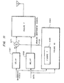
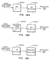
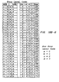
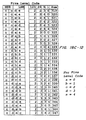
- FIGURE 1 is a representation of the composite NTSC television spectrum, as used in the United States (Type M).
- the visual signaling for NTSC analog transmission for broadcast purposes utilizes vestigial sideband amplitude modulation for the impression of the visual information onto the visual carrier signal.
- a filter, tailored to the characteristics of the vestigial sideband modulation, and an amplitude modulation detector detect the visual information embedded in the signal.
- FIGURE 1a The television vestigial sideband "VSB" signal is shown in FIGURE 1a.
- This FIGURE is normalized to the visual carrier frequency 102, which is shown in the FIGURE as 0.0 MHz. Because the television signal is vestigial sideband, it is neither all double sideband nor is it all single sideband. Baseband frequencies from zero Hz to 0.75 MHz are modulated in full double sideband and appear in the normalized spectrum of FIGURE 1a as the region 104 from (-0.75 MHz to +0.75 MHz).
- Baseband frequencies from (1.25 MHz to 4.08 MHz) are modulated in single sideband and appear in the normalized spectrum of FIGURE 1a as the region 106 from (+1.25 MHz to +4.08 MHz).
- Baseband frequencies from (0.75 MHz to 1.25 MHz) are transmitted in transition regions and appear in the normalized spectrum of FIGURE 1a as the regions 108 from (-1.25 MHz to -0.75 MHz) and from (+0.75 MHz to +1.25 MHz) which is neither double sideband nor single sideband.
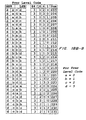
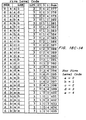
- FIGURE 1b displays the output of an idealized detector that would be realized by multiplying the spectrum of FIGURE 1a (located at some carrier frequency) by a cosine wave of that same carrier frequency and phase.
- the signal energy in a region 110 below 0.75 MHz is 6 dB above the energy in the signal at frequencies above 1.25 MHz. Twice the voltage is present in the received signal because that portion of the spectrum is double sideband modulated.
- the region 112 above 1.25 MHz has normal amplitude because it is from the single sideband region.
- the transition region from 0.75 MHz to 1.25 MHz also has more energy than the normal level.
- the receiver employs a filter, called a Nyquist filter, as shown in idealized form and normalized to zero frequency (as was the spectrum of FIGURE 1a) in FIGURE 1c.
- This filter is normally inserted in the receiver prior to detection, and shapes the spectrum to give equal treatment to all frequencies carried in the signal.
- the Nyquist filter aggressively attenuates the signals that are more than 0.75 MHz below the picture carrier and, in this example, linearly attenuates the signals in a region 114 at frequencies between 0.75 MHz below the picture carrier and 0.75 MHz above the picture carrier.
- the signal is one half of its original value (6 dB attenuation).
- the amplitude characteristic of the Nyquist filter is anti-symmetric about the carrier frequency.
- filters with an anti-symmetric characteristics are termed Nyquist filters. While this example shows a linear amplitude characteristic in the region 114 from (-0.75 MHz) to (+0.75 MHz), the requirement is that the filter characteristic be anti-symmetric about the carrier frequency normalized to zero in FIGURE 1c. The consequence of such a filter is that it yields a flat output in the detected signal from zero Hz to the upper end of the band.
- the horizontal dashed line 118 of FIGURE 1b displays the amplitude of the output spectrum of the Nyquist filter of FIGURE 1c.
- Practical television receivers utilize a typical response 120 more like that shown in FIGURE 1c. The amplitude of the upper band edge is rolled off in the color region to minimize the cross talk between the color signal and the luminance signal and to make the filter design easier.
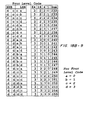
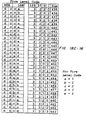
- FIGURE 1d is a representation of the "compatible" stereo Aural signal used in NTSC television.
- the amplitudes are not to scale; the spectral occupancies of the components of the signal are emphasized.
- the (L+R) channel 122 occupying 0 to 15 kHz in the baseband spectrum preserves the monophonic reception to non-BTSC receivers.
- the pilot carrier 124 is transmitted at the horizontal frequency rate (15,734 Hz). The purpose of the pilot carrier is to permit detection of the presence of a stereo signal and to permit recovery of the information carried within the other sub-carriers of the BTSC signal.
- the (L-R) 126 region is a double sideband amplitude modulated suppressed carrier signal with special signal processing to reduce the effects of noise.
- the Separate Aural Program ("SAP") at 128 is a double sideband frequency modulated signal permitting the transmission of additional Aural programming for purposes such as second language.
- the SAP has a somewhat reduced frequency response; limited to 10 kHz.
- the Professional Channel 130 is a lower quality channel that can be used for the transmission of audio or low speed telemetry.
- the encoding of the present invention is rendered so that its information is not materially present in the video output of conventional television receivers.
- a receiver for NTSC analog television video must compensate for the effects of the vestigial sideband modulation of the transmitter. This compensation reduces the detected amplitude of those frequencies which are double sideband; i.e. baseband frequencies between zero and 750 kHz.
- Such compensation is provided by a filter (commonly known as the Nyquist filter) before the detector, where the IF signal is inverted from the broadcast spectrum and where the amplitude response is zero attenuation at plus 750 kHz from the visual carrier, one-half (-6dB) at the visual carrier and approaching zero at minus 750 kHz.
- a filter commonly known as the Nyquist filter
- the present invention creates sidebands about an optionally suppressed carrier which is in quadrature to the visual carrier.
- This group of sidebands carry the present invention's visual data signal and is independent of the sidebands bearing the NTSC signal.
- the present invention's visual data signal sidebands exist in the double sideband frequency region of the NTSC signal".
- This invention identifies two methods for accomplishing this object. One of these methods is known as the phase modulation method wherein the data signal is applied through phase modulation of the visual carrier.
- Another embodiment is known as the additive technique, whereby the quadrature sidebands carrying the data signal are derived from an independent generator and combined additively to the analog visual signal.
- the data signal to be added includes equal and opposite amplitude correction to cancel the effects caused by the receiver's Nyquist filter. This is accomplished with a Compensation Subsystem.
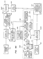
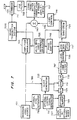
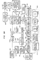
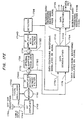
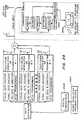
- FIGURE 2 is a block diagram of a prior art television transmitter.
- a source of baseband video 201 presents a visual signal to one input of an Amplitude Modulator 203.
- This AM modulator is typically configured to produce only negative modulation (i.e. the carrier is most attenuated at white levels and least attenuated during the synchronization pulses) in NTSC and similar television systems.
- the video may come from, for example, a conventional television camera, video playback device, or relayed from another location.
- the other input to the Amplitude Modulator 203 comes from a Visual Reference Oscillator 205 shown here, by example, as a 45.75 MHz source.
- the low level amplitude-modulated visual signal from Modulator 203 is applied to a Visual Transmitter 207 where it is translated from the IF frequency of the Amplitude Modulator 203 to the transmission frequency. Also, the Visual Transmitter 207 increases the power level to levels sufficient for reaching the intended viewers.
- This amplitude modulated signal with equal intensity sidebands is applied to a VSB Filter 209 that shapes the spectrum so it appears as shown in FIGURE 1a. This signal is then applied to one input of Combiner 211.
- a baseband Aural source 213 presents an Aural signal to one input of a Sound FM Modulator 215.
- the source of the audio is related to the source of the video.
- a Sound Reference Oscillator 217 at a frequency 4.5 MHz lower than the Visual Reference Oscillator 205 provides the other input to FM Modulator 215.
- Sound References Oscillator 217 is shown as (45.75 - 4.5) MHz cosine wave source 217. This source is coupled to the Visual Reference Oscillator 205 by connection 219 to insure that the video and sound sources are frequency-synchronized.
- the output of the Sound FM Modulator 215 is applied to a Sound Transmitter 221 where its frequency is translated from the IF frequency of the Sound FM Modulator 215 to the transmission frequency. Also, the Sound Transmitter 221 increases the power level to levels sufficient for reaching the intended viewers. This signal is then applied to the other input of Combiner 211 where it is joined to the visual signal. The combined signal is applied to an Antenna 223 that radiates the signal to the intended receivers.
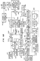
- FIGURE 3 is a block diagram of a prior art television receiver.
- Antenna terminal 340 is connected either to a cable television input 344 or an antenna 346 for receiving radiated television signals.
- Other sources of television signals such as for example from pre-recorded media, satellite receivers, microwave receivers are possible as well.
- the input signal is conveyed to an RF amplifier 348 that increases the strength of the signal to levels sufficient for use by the subsequent circuits.
- the signal is then applied to one input of a Mixer 350 that shifts the desired signal to the pass band of the IF amplifier 354 which follows further down the signal path. The spectrum is reversed in this process placing the aural carrier at a lower frequency than the visual carrier.
- the other input to Mixer 350 is provided by Local Oscillator 352.
- the frequency of the Local Oscillator 352 is adjusted to cause the desired channel's spectrum to be translated to the pass band of the IF amplifier 354.
- the signal is then applied to Optional Adaptive Equalizer 356.
- the Optional Adaptive Equalizer 356 is not required for the operation of the receiver. Nevertheless, under conditions of multi-path and certain other types of distortion, the Optional Adaptive Equalizer 356 can significantly improve the reception.
- the Optional Adaptive Equalizer 356 may also be implemented at baseband frequencies after Detector 358, but with considerably more difficulty and expense.
- the IF Amplifier 354 also includes a Nyquist Filter with characteristic as shown in FIGURE 1c. The amplified and filtered signal spectrum is then applied to Detector 358.
- Detector 358 is an amplitude detector that may be an envelope detector, a synchronous detector, or a detector that exhibits varying amounts of the properties of these types of detectors.
- One output of the Detector 358 is a baseband signal which is then applied to Video Processor 360 which prepares the various components of the signal for producing a picture on Video Display Device 362.
- the other output of the Detector 358 is applied to a Limiter 364 which strips off any amplitude modulation that may exist on the aural signal.
- the signal then contains only frequency modulation and is applied to an FM detector 366.
- the output of the FM Detector 366 is a baseband Aural signal that is applied to Audio Amplifier 368
- the signal from the Audio Amplifier 368 drives Sound Reproducer 370.
- the previously described aural recovery technique is called the "inter-carrier sound” method.
- the television signal undergoes substantial processing - especially in cable systems - which shifts (heterodynes) it to various frequencies.
- the local oscillators also known as converters
- the heterodyne processors are not perfect, they have phase instabilities which modulate both the visual and aural carriers.
- the inter-carrier receiver principle takes advantage of the precise frequency difference between the visual and aural carriers to bring the audio signal to baseband. Since the local oscillators in the various processors affect both carriers the same way, the inter-carrier principle nulls out these disturbances. This is analogous to "common mode rejection" in differential amplifiers.
- a variation of the previously described aural recovery technique is called the "split sound" method.
- the aural component is extracted from the IF signal prior to detector 358. This signal is subjected to limiting to remove incidental AM components and presented to an FM detector similar to that shown at 366.
- the aural signal When “split sound” techniques are applied, the aural signal is not dependent upon any properties of the visual carrier. While the aural carrier is free from properties of the visual carrier, it becomes dependent upon the accumulated instability of processing oscillators (heterodyning) along the signal chain. These sources of instability would include the transmitter, cable heterodyne processors and the local oscillators of intervening frequency translation devices, such as cable subscriber terminal devices and the tuner of the TV itself.
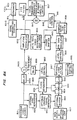
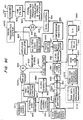
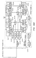
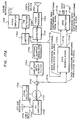
- FIGURE 4a is a representation of a television transmitter (the generic term “transmitter” describes broadcast transmitters as well as cable and other modulators) including data encoder 425, according to a first preferred embodiment of the present invention.
- the transmitter of FIGURE 4a includes a data source 427 (Return to Zero, RZ, or Non Return to Zero, NRZ), Serial to Parallel converter “S/P” 429, Digital signal to Analog signal (“D/A”) converter 431, Low Pass Filter (LPF) 432, Level Control 435, Clock circuit, 433, Phase Modulator 437, Compensator Subsystem 439, Level Control 441, and a Visual Reference Oscillator 405 at some suitable frequency, here shown by example as 45.75 MHz.
- D/A Digital signal to Analog signal
- LPF Low Pass Filter
- the Data Source 427 optionally includes either software or hardware to randomize the data so that it contains essentially equal numbers of logic one values and logic zero values. This randomization is then undone in the receiver yielding the original data.
- Such hardware and software is well known in these arts. Residual zero frequency and near-zero frequency (d.c.) components generated by an asymmetrical amount of logic ones and logic zeros can produce undesirable artifacts which are discussed more completely elsewhere.
- FIGURE 4a illustrates an apparatus, systems and methods, wherein the visual carrier is first impressed with the data in a special manner according to this invention and then modulated with video in the normal manner of NTSC practice.
- the visual signal from the Baseband Video Source 401 is modulated by an Amplitude Modulator 403a onto the visual carrier provided at terminal 445 which has the data signal already impressed upon it by data encoder 425. This is presented to the Visual Transmitter 407 which translates the signal to the radiated frequency and amplifies it to a power level sufficient for radiation. The signal is then passed on to the VSB Filter 409 which shapes the spectrum according to FIGURE 1a and conveys it to one of the inputs of Combiner 411.
- the Baseband Sound Source 413 signal is applied to one input of the Sound FM Modulator 415.
- the other input to the Sound FM Modulator 415 comes from the Sound Reference Oscillator 417 which is coupled by connection 419 to the Video Reference Oscillator 405 indirectly through Phase Modulator 437 so as to provide a sound reference oscillator which is always 4.5 MHz below the instantaneous visual carrier frequency.
- the Sound Transmitter 421 translates the spectrum to the desired output channel frequency before applying it to the other terminal of combiner 411 which adds the FM sound signal to the visual signal before passing it on to the antenna 423 for radiation.
- This example illustrates the phase modulated data applied prior to the visual modulation.
- the opposite order is also valid because the properties of each modulation system are multiplicative.
- the transmitter described is sometimes referred to as "low level modulation". That is because the visual signal (and in this case the data signal as well) is applied to a stage in the transmitter in advance of its final power amplification. Under these conditions, each additional stage from the point where modulation is first applied should be operated in a linear mode. In this example, a frequency translation and spectral inversion occurs within the Visual Transmitter 407 of FIGURE 4a, to place the IF signal on the appropriate RF frequency.
- phase modulation process described above could also be applied to the oscillator in the Visual Transmitter 407 which is used for translating the visual signal from the IF frequency to its desired RF frequency provided however, that consideration is made to the relationship and amplitude of the sidebands with respect to the final output signal and that a signal including the phase modulation information is made available at the appropriate frequency to block 417 to maintain the intercarrier sound relationship of 4.5 MHz.
- the visual signal is applied to the last active power stage of the visual transmitter.
- This requires substantial amounts of visual signal.
- no power stages of the transmitter are required to be operated in their linear mode, permitting more efficient and higher power RF amplification.
- the encoded data signal can be combined at many places within a television transmitter of this design and / or its combiner or antenna transmission line provided that the stages subsequent to the injection of the phase modulation are linear and of sufficient bandwidth to pass the encoded data signal. From the foregoing example it can be seen that there are a number of theoretical and practical implementations at the disposal of one skilled in the art to permit the effective combining of the encoded data signal and the visual modulation.
- the Visual Reference Oscillator 405 generates an IF signal, designated as f IF , by any of the many methods well known to those skilled in these arts.
- f IF an IF signal
- a crystal oscillator in the 718Y series produced by Vectron Laboratories of Norwalk Connecticut with Internet Web Site: www.vectron-vti.com operated in the normal manner intended by its manufacturer could be used for this purpose.
- This signal would normally be a stable, pure cosine wave of frequency f IF .
- This signal is then introduced into a phase modulator 437 whose design is conventional and well understood by those of normal skill in the art.
- a circuit can be derived using two-way ninety degree power splitter such as the PSCQ2-50 sold by Mini-Circuits Inc. of Brooklyn, New York with Internet Web Site: www.minicircuits.com, which will permit it to operate as a phase modulator at this frequency.
- Complete phase modulator subsystems are available from several sources including Anaren Microwave Inc of East Syracuse, New York with Internet Web Site: www.anaren.com.
- the phase modulator 437 is driven by the signal supplied through LPF 432 which band limits the frequencies of the data signal and conveys it to Level Control 4.1 435 after which the signal is passed to the left input terminals of the phase modulator 437 in FIGURE 4a.
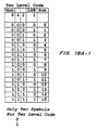
- Phase Modulator 437 If only two phases are modulated, just a single data bit is present at one time on the appropriate terminals of Phase Modulator 437 and the S/P converter 429 and the converter D/A 431 perform a trivial version of their normal tasks or can be omitted.
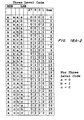
- Clock circuit 433 steps the data through the S/P converter 429 and D/A converter 431 as required by such designs. If four phases are modulated by Phase Modulator 437, two consecutive bits are converted to parallel form by S/P converter 429 and presented simultaneously to the D/A converter 431 which converts them into appropriate four level analog signals for input to the Phase Modulator 437.
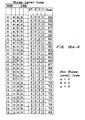
- Phase Modulator 437 If eight phases are modulated by Phase Modulator 437, three consecutive bits are converted to parallel form by S/P converter 429 and presented simultaneously to the D/A converter 431 which converts them into appropriate eight level analog signals for input to the Phase Modulator 437.
- the output of the phase modulator is then passed to the Compensator Subsystem 439 of FIGURE 4a. Data is similarly passed to the compensator subsystem 439 for other numbers of phases.
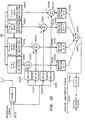
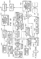
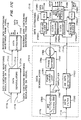
- the Compensator Subsystem 439 of FIGURE 4a is shown in more detail in FIGURE 4b.
- the Compensator Subsystem consist of circuitry for adjust the amplitudes and phases of the sidebands created in the modulating process. It includes a Nyquist Filter 451 designed using normal methods well known by those of ordinary skill in these arts. As just one example, a surface wave filter operated in the normal manner intended by its manufacturer Sawtek Corporation of Orlando, Florida with Internet Web Site: www.sawtek.com, could be used for this purpose. A filter could be designed and constructed out of discrete components such as inductors and capacitors using a filter design software program such as provided by Eagleware of Norcross, Georgia with Internet Web Site: www.eagleware.com.
- the amplitude versus frequency characteristic of the Nyquist Filter 451 is the same as would be found in a normal NTSC television receiver and has the same characteristic as is shown in FIGURE 1c.
- the output spectrum of the Nyquist Filter 451 is shown in schematic form in FIGURE 4c at 471.
- the bold capital letters, A through F in FIGURES 4b through 4e correspond to frequency components in the spectrum and the places where they can be found in the circuit of FIGURE 4b.
- the Nyquist Filter 451 adjusts the amplitude versus frequency spectrum of the IF frequency which is modulated with data.
- the spectrum has experienced the same processing as if it had passed through the IF Amplifier including Nyquist Filter 354 of an ordinary television receiver, such as depicted in FIGURE 3.
- the resulting shaped spectrum signal is double sideband modulated in Mixer #1 453 upwards in frequency using a Local Oscillator #1 455 whose frequency is an exact multiple (N) of the IF reference frequency, f IF . This is shown as the frequency component 473 in FIGURE 4d.
- Connection 457 between Visual Reference Oscillator 405 of FIGURE 4a and the Local Oscillator #1 455 ensures that the Local Oscillator #1 455 is at an exact multiple, N, times the IF reference frequency and phase relationships are preserved.
- the structure of Mixer #1 453 is well understood by those of ordinary skill in the art and a variety of satisfactory implementations are well known.
- Mini-Circuits SRA-1 module operated in the normal manner intended by its manufacturer, Mini-Circuits of Brooklyn, New York, could be used for this purpose.
- the structure of Local Oscillator #1 455 is well understood by those of ordinary skill in the art and a variety of satisfactory implementations are well known.
- a Vectron circuit and operated in the normal manner intended by its manufacturer could be used for this purpose.
- the upper sideband 477 and lower sideband 475 in FIGURE 4d are mirror images of each other
- the upper sideband 477 in FIGURE 4d is merely a frequency translated version of the output 471 in FIGURE 4c of the Nyquist filter 451.
- the combination of the translated signal 473, 475, and 477 in FIGURE 4d is then filtered by Band Pass Filter, BPF # 1, 459 at frequency (N+1)*f IF to remove the undesired frequency components 473 and 475 in FIGURE 4d which are found at the output of the Mixer #1 453.
- the upper sideband 477 in FIGURE 4d survives and is a replica of the original data spectrum 471 in FIGURE 4a but now located at a different frequency.
- Band Pass Filter #1 459 is designed and constructed using techniques well known to anyone skilled in these arts. Commercially available software packages compute the elements necessary to build filters such as BPF Filter # 1 459. One such filter design program is provided by Eagleware of Norcross, Georgia. Additionally, BPF #1 459 can be purchased commercially from suppliers of such filters such as Microwave Filter Company of East Syracuse, New York with Internet Web Site: www.klmicrowave.com. The process is now repeated with Mixer # 2 461, Local Oscillator #2 463, and Band Pass Filter #2 465.
- the translated signal 479 in FIGURE 4e is then filtered by Band Pass Filter BPF #2, 465 at frequency f IF to remove the undesired frequency components 481 and 483 in FIGURE 4e found at the output of the Mixer # 2 461.
- the lower sideband 479 in FIGURE 4e survives and is a replica of the original phase modulated and shaped signal 471 in FIGURE 4a but inverted in frequency. Compare 479 in FIGURE 4e with 471 in FIGURE 4a.
- Band Pass Filter #2 465 is designed and constructed using techniques well known to anyone skilled in these arts. Commercially available software packages compute the elements necessary to build filters such as BPF Filter # 2 465.
- One such filter design program is provided by Eagleware of Norcross, Georgia.
- BPF #2 465 can be purchased commercially from suppliers of such filters. This signal has been preshaped (compensated) so that when it is processed by the IF Amplifier including Nyquist Filter 354 in FIGURE 3 found in the receiving device the spectral shaping caused by that Nyquist filter will be effectively negated. If the receiver employs a well designed visual detector, its output will contain no additional amplitude modulation components resulting from the data. Picture degradation will be avoided.
- the present invention does not use an Inverse Nyquist filter at the signal source. Instead it uses a Nyquist filter and a spectrum processing means to predistort the signal. This is important because the characteristic shape of a Nyquist filter is not defined. Rather, a Nyquist filter is one which has an anti-symmetric characteristic around its Nyquist frequency. This characteristic may be linear, but it does not have to be. An infinite number of possible characteristics can satisfy the Nyquist criterion. By using a Nyquist filter in the signal source, it becomes convenient to use a filter representative of the population of receivers exposed to the present invention's signal. This is accomplished by simply using the commercially available Nyquist filter most commonly used in those receivers.
- Phase Modulation When Phase Modulation is used to embed the data, the resultant visual carrier amplitude is unchanged.
- a perfect envelope detector will not respond to the data modulation.
- a synchronous detector responds to the projection of the resultant vector on the real axis. This vector changes in relation to the data modulation.
- FIGURE 5a is a representation of a television transmitter including data encoder 525, according to a second preferred embodiment of the present invention.
- FIGURE 5A includes a Data Source (Return to Zero, RZ, or Non Return to Zero, NRZ) with optional Randomizer 527, Serial to Parallel (“S/P") converter, 529, Digital signal to Analog signal converter, 531, LPF 532, Level Control 535, Clock circuit, 533, Double Side Band (DSB) Data Modulator 537 and Compensator Subsystem 539.
- S/P Serial to Parallel
- DFB Double Side Band
- FIGURE 5A illustrates an apparatus, wherein sidebands of an optionally suppressed carrier which is in quadrature with the visual carrier are modulated in a special manner according to this invention and then is adjusted in strength in Level Control 541 and then combined in Combiner 547 with the visual carrier which is modulated with video in the normal manner of NTSC (or other television standard) practice.
- the combination of the normally modulated visual carrier and the sidebands modulated with data according to this invention and placed in quadrature with the visual carrier is presented to the Visual Transmitter 507 for translation to the frequency of the channel utilized and is amplified.
- the combination of the modulated visual signal and the data signal is passed through the VSB Filter 509 before being combined with the aural signal in Combiner 511 and passed to Antenna 523 for radiation.
- the Phase Shifter 543 imparts additional phase shift as necessary so that the phase relationship of the optionally suppressed carrier of the data sidebands presented to Combiner 547 on line 545 is in quadrature to the visual carrier presented to Amplitude Modulator 503.
- the propagation lengths of the various components in this immediate area and their interconnecting cables all influence the phasing of the signals arriving at Combiner 547.
- the correct adjustment of Phase Shifter 543 reconciles these phase properties by placing the two signals (analog visual and data) in quadrature, one to another. This relationship can be observed and adjusted through the simultaneous oscilloscopic observation of the incident and quadrature components of a synchronous detector placed after a Nyquist filter.
- the output of the Compensator Subsystem 539 found on line 545 can be applied at any place in the visual transmitter chain after its Amplitude Modulator 503 provided, however, that its phase and power are appropriately matched to the circuit. Moreover, the signal could be combined spatially through a separate antenna system provided that the amplitude and phasing considerations previously mentioned were satisfied.
- the encoded data signal could be added to the frequency translation oscillator output provided that appropriate considerations are observed regarding the relationship and amplitude of the sidebands with respect to the final output signal.
- the properties of the compensator subsystem 539 could likewise be distributed throughout the heterodyning elements of the visual transmitter identified in block 507 provided, however, that the appropriate considerations as to sideband amplitudes were preserved.
- the encoded data signal may be added to any stage in the transmitter provided that no subsequent frequency multiplication occurs and that all stages subsequent to the encoded signal injection are linear and of sufficient bandwidth that the sideband structure is preserved.
- a Visual Reference Oscillator 505 at an intermediate frequency designated as f IF may be constructed by any of the many methods well known to those skilled in these arts.
- f IF intermediate frequency
- This signal would normally be a stable, pure sine wave of frequency f IF .
- This signal is then phase shifted in Phase Shifter 543 as necessary and then introduced into DSB Data Modulator 537 whose design is conventional and well understood by those of normal skill in these arts.
- a double balanced Mixer such as the Mini-Circuits SRA-1 module operated in the normal manner intended by its manufacturer could be used for this purpose
- the DSB Data Modulator 537 is driven by the data signal through LPF 532 which band limits the frequencies of the data signal and coveys it to Level Control 535 after which the signal is passed to the input terminal of the DSB Data Modulator 537. If only two levels are modulated, just a single data bit is present at one time on the appropriate terminals of DSB Data Modulator 537 and the S/P converter 529 and the D/A converter 531 perform reduced tasks or can be deleted.
- Clock circuit 533 steps the data through the S/P converter 529 and D/A converter 531 units as required by such designs.
- DSB Data Modulator 537 If four levels are modulated by DSB Data Modulator 537, two consecutive bits are converted to parallel form by S/P converter 529 and presented simultaneously to the D / A converter 531 which converts them into appropriate four level analog signals for input to the DSB Data Modulator 537. If eight levels are modulated by DSB Data Modulator 537, three consecutive bits are converted to parallel form by S/P 529 and presented simultaneously to the D/A 531 which converts them into appropriate eight level analog signals for input to the DSB Data Modulator 537. The D/A converter converts bits similarly for other numbers of levels.
- the output of the DSB Data Modulator 537 is then passed to the Compensator Subsystem 539 which is identical to that of the Compensator Subsystem 439 FIGURE 4b.
- This signal has been preshaped (compensated) so that when it is processed by the IF Amplifier including Nyquist Filter 354 in FIGURE 3 found in the receiving device, the spectral shaping caused by that Nyquist filter will be effectively negated. If the receiver employs a well designed visual detector, its output will contain no additional amplitude modulation components resulting from the data. Picture degradation will be avoided:
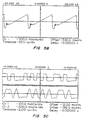
- FIGURE 5b is the actual voltage waveform of NTSC baseband video out of Baseband Video Source 501.
- the top trace of FIGURE 5c is the actual voltage waveform of two-level data at the output of Data Source 527 and the bottom trace of FIGURE 5c is the actual voltage waveform at the output of Low Pass Filter 532. Note the time delay through the filter.
- FIGURE 5d is an actual spectrograph of the output of DSB Data Modulator 537 due to double sideband modulated NRZ data.
- FIGURE 5e is an actual spectrograph of data signal at output of Compensator Subsystem 539 due to NRZ data.
- FIGURE 5f is an actual spectrograph at the output of Visual Transmitter 507 but before VSB Filter 509. The top trace is of ordinary NTSC and the lower trace is of the Visual Data Signal.
- Figure 5g is an actual spectrograph after VSB Filter 509. The upper trace is the NTSC signal and the lower trace is the visual data signal.
- the resultant vector's amplitude changes.
- the resultant vector is the Pythagorean solution of the instantaneous amplitude of the visual components and the data component.
- the length of the projection of the resultant vector along the real axis is unchanged.
- a perfect synchronous detector will not respond to the data modulation; however, an envelope detector will respond to the changing strength of the resultant vector.
- the present invention's data signal is double sideband amplitude modulated onto an optionally suppressed carrier which is in quadrature phase with the picture carrier. If both the video signal and the present invention's signal were normal double sideband, they could be separated with synchronous detectors by conventional methods. Since the television signal is not all double sideband, but vestigial sideband, a television receiver includes a Nyquist slope filter to properly weight the upper and lower video sidebands around the carrier so that the correct amplitude is available for detection. In the course of its normal functions, this filter would convert a plain double sideband modulated signal (with opposite sidebands equal in amplitude to each other) into a double sideband signal with asymmetrical sidebands.
- This newly formed asymmetrical sideband set would have an undesired component in phase with the video carrier.
- the data sidebands were initially placed on an optionally suppressed carrier which is in quadrature to the picture carrier at the origination point of the signal, after being operated on by the receiver's Nyquist filter, a detector operating on the video signal would include unwanted components from the data sidebands. This is because the effects of the Nyquist filter -- which is essential for preservation of the RA relationship of the visual signal - and are unnecessary and undesirable for the present invention's data signal. Consequently, quadularity would not be preserved between the visual carrier and the present invention's signal.
- This problem can be averted by properly shaping the spectrum of the present invention's data signal so that when it passes through the receiver's Nyquist filter, a double sideband spectrum in quadrature with the visual carrier and possessing equal amplitude sidebands will be obtained. Under these conditions, there will be no PM to AM conversion and minimal cross coupling of the quadrature signal's energy will be presented to the receiver's video detector. Therefore the receiver's detector will respond essentially only to the video signal. If the receiver utilizes a synchronous or similar behaving detector which inherently is immune to quadrature components, the present invention's signal will be essentially ignored.
- the pre-shaping of the present invention's data signal is done with a compensation network which includes a Nyquist filter representative of those found in the population of receivers exposed to the present invention's signal.
- a composite signal optimizing the result can be implemented either with a parallel configuration of Nyquist filters fed with signal strengths in proportion to the numbers of the respective filters in the population or with a Nyquist filter designed to optimize the result using standard filter synthesis techniques.
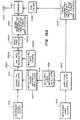
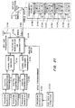
- FIGURE 6a is a block diagram of a television transmitter, according to a third preferred embodiment of the present invention.
- the transmitter combines the techniques of the transmitters illustrated in FIGURE 4 and FIGURE 5A.
- a degree of phase modulation and a degree of addition of quadrature sidebands are employed to optimize the result.
- the reference oscillator signals delivered to all portions of the additive system is derived from the instantaneous frequency and phase found at the output of the phase modulator 637a.
- Only two new elements are introduced in FIGURE 6. All other elements are found in either FIGURE 4a or FIGURE 5A (or both) and have the same functions and structures as previously described.
- the two new elements are Delay Element 649a and Delay Element 649b.
- delay elements The purpose of these delay elements is to ensure that the embedding of data as phase modulation and the embedding of data in quadrature sidebands are properly timed. Since the propagation time through the various circuit elements in FIGURE 6 depends on the details of their designs, the delay elements will have different values of delay for the various possible implementations.
- the delay elements can be implemented in a variety of techniques including, for example, by transmission lines or by a digital delay element preceded by an A/D converter and followed by a D/A converter. These are all means familiar to those skilled in these arts. It will be clear to those skilled in these arts that the precise location of Delay Element 649a and of Delay Element 649b in their respective signal paths is inconsequential. It is possible to locate the delay elements anywhere along their respective paths without changing the effect of the delay on the operation of the system. Some locations may be easier to implement than others.
- the system of FIGURE 6b utilizes two different Data Sources for the phase modulation and additive approaches. In environments relatively free of noise, distortion, and interference, it will be possible to carry even larger amounts of data using these two modes of modulation for separate data signals rather than as a reinforcing mechanism as shown in FIGURE 6a.
- the basis of an essential element of the present invention's techniques is the ability to maintain a signal carrying data in an information space which is not materially interfered by nor interfering to the information space delivering the NTSC television signal. This process is more complex than it might first appear. It is well appreciated that a signal can be placed in quadrature to a double sideband signal. This is the basis of the QAM (Quadrature Amplitude Modulation) system used widely throughout telecommunications networks and one of the fundamentals enabling color to be compatibly added to the NTSC television standard. The issue associated with maintaining a signal in quadrature with an NTSC television's visual signal is more complex.
- QAM Quadratture Amplitude Modulation
- the NTSC visual signal operates with three separate and distinct modulation properties: first is an area were the amplitude of both the upper and lower sidebands is equal. This region is called the double sideband region 104 of FIGURE 1a. The second area is one in which the amplitude of the lower sideband spectra is being attenuated. The region is known as the transition region 108 of FIGURE 1a. The third region in that portion of the spectrum where only the upper sideband energy is transmitted. The region is called the single sideband region 106 of FIGURE 1a.
- the practical circuitry required to shape the television signal to conform to these regions for broadcast introduces several unintentional consequences onto the television signal:
- One principle of VSB transmission is predicated upon the double sideband region of the television spectrum being centered along the slope called the receiver's Nyquist filter.
- the double energy transmitted in the double sideband region 104 of FIGURE 1a is undone by the Nyquist filter, thereby restoring the recovered television signal to one of more or less flat amplitude response across its multi-octave spectrum.
- the Vestigial Sideband filter in the transmitter and the Nyquist filter in the television receiver are realized in real-world elements they generally produce subtle variations in the amplitude and phase of the signals carried through them.
- phase correction in the data signal's path so as to reposition the sidebands in the area operated upon by the correction circuit to the intended position of quadularity.
- This correction can normalize the errors of the VSB filter, visual transmitter and broadly replicate the typical phase errors found in the many Nyquist filters in the television's which are part of the reception population.
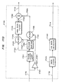
- FIGURE 7 combines all of the sound processing elements in one block, the Sound Transmitter System 721a.
- Proper selection of Clock Generator 733 frequency and synchronization of that frequency to the Baseband Video through connection 785 and the use of an optional comb filter 787, can localize the data spectrum of the quadrature sidebands so that they interleave with the spectrum of the video. These methods are well known by those skilled in these arts and are the same methods used to interleave the color signal spectrum into the gaps of the luminance signal spectrum.
- the clock frequency from Clock Generator 733 can be selected to be an odd multiple of half the line scanning rate to accomplish these objectives. This will further reduce any residual interference.
- Connection 785 conveys the baseband visual signal to Clock Generator 733.
- the baseband visual signal includes the color sub-carrier and horizontal synchronization pulses.
- Optional Comb Filter 787 will further attenuate any spectral components of the data signal that remain in conflict with the visual spectrum. The degree of removal of these spectral components must be balanced against the reduction in reliability of data recovery. A compromise is struck between reduction of visibility in existing receivers and the robustness of the data for new data receivers.
- Comb filters such as Optional Comb Filter 787 are commonly used in television processing, origination and reception equipment. They are often constructed with tapped surface acoustic delay lines or with digital techniques and are well known to those skilled in these arts.
- the timing of the scanning of the image may be perturbed. This would result in a small displacement of the scan line with respect to the transmitted synchronizing pulse. In those cases where this phenomenon operates on the effective synchronization timing, the result is manifest as ragged vertical edges. Under these circumstances, the effect can be alleviated by holding the data signal to a known state during the critical synchronization transitions. Adoption of this technique would result in a reduction of data throughput of approximately a quarter of a percent. The resulting uneven flow of data into the system needs to be controlled at the proper time relative to the synchronization pulses.
- the data flow is regulated in an Optional Data Buffer 789, under the control of an Optional Control Signal Generator 791 which is timed by an Optional Sync Separator 793.
- Optional Control Signal Generator 791 which is timed by an Optional Sync Separator 793.
- the Optional Sync Separator 793 identifies the times during which the data should be held to a known state.
- the Optional Control Signal Generator 791 generates timing signals which are passed to the Clock Generator 733 and the Optional Buffer 789 to store the data during this time interval and to stop the passage of data through the S/P 729 and the D/A 731 blocks.
- Level Control 735 adjusts the depth of modulation of data imposed on the quadrature signal by DSB Data Modulator 737.
- Level Control 741 adjusts the amount of data injected into the composite video channel. In practice, this level is adjusted for the minimum amount of data signal (plus some margin) necessary to reach the SNR objectives of the service area. Only this minimum is used in order to minimize any impact the data signal may have on the visual signal. This data signal level may be different in a cable system than over the air.
- the S/P 729 and A/D 731 are not needed if only two states of data (one logic bit) are modulated. These units are necessary for more states.
- abatement signal into the visual signal (injecting the abatement signal into the visual carrier) at baseband itself or into the visual signal at some appropriate RF frequency.
- the abatement signal will tend to cancel or at least reduce (abate) the interference to the video in receivers using classes of detectors manifesting susceptibility to this phenomenon.
- FIGURE 8a includes all of the elements of FIGURE 7 and adds waveform shaping circuits and delay circuits to introduce an abatement signal into the baseband video. This will tend to cancel or abate the interference from the data signal contributed to the video through the detection process mentioned above. As previously mentioned, it can also be seen that this correction signal could be introduced in the RF domain provided that the shaping and delay were appropriate to bring about abatement.
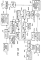
- FIGURE 8a is a block diagram of a transmitter according to an additional embodiment.
- Wave Shaping Circuits 895 take the analog wave forms presented to the DSB Data Modulator 837 (through Level Control 835) and appropriately shape the waveforms so that when they are subtracted from the visual waveform, an improved result will be obtained. Receivers utilizing detectors of the classes referred to above, will experience less impaired video.
- the output of the Wave Shaping Circuits 895 is adjusted in amplitude by Level Control 897, and, if necessary, delayed in time by Delay 899 before being combined with the analog baseband video in Combiner 8103. This Analog Abatement Signal 8101 appears on one of the input terminals of Combiner 8103.
- Delay element 8105 Depending on the propagation times of the signals through the various paths, it may be necessary to delay the video with Delay element 8105 or to delay the abatement signal with Delay element 899. It will be appreciated that the exact location of the Delay Element 8105 and Delay Element899 along their respective signal paths is of no consequence. They may be placed elsewhere and produce the same result.
- the delay elements and level adjustment elements are conventional structures well known to those skilled in these arts and can be implemented in a wide variety of forms, any of which will serve these purposes, provided that the considerations discussed above have been met.
- Delay elements can be implemented with appropriate lengths of transmission lines or using digital techniques where the analog signal is converted to digital form, delayed using digital memory devices, and then converted back to analog form. More will be said below about the wave shaping circuits, 895.
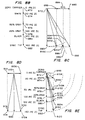
- FIGURE 8b illustrates the luminance signal at the instant in time when the carrier and sideband vectors are in alignment.
- Point 872 is the zero carrier location.
- Point 874 is the sum of the carrier and the sidebands when the visual signal is white.
- Point 876 is the sum of the carrier and the sidebands when the visual signal is at 50% gray.
- Point 878 is the sum of the carrier and the sidebands when the visual signal is at 20% gray.
- Point 880 is the sum of the carrier and the sidebands when the visual signal is black (blanking level).
- Point 882 is the sum of the carrier and the sidebands when the visual signal is at sync tip.
- the maximum length of the signal vector is the distance between the zero carrier point 872 and the sync tip point 882.
- the scale used to describe modulation in the NTSC waveform divides the area between black and white into one hundred equal divisions frequently referred to as Institute of Radio Engineers ("IRE") units. If one were to extend that scale in the RF domain, from the level referred to as white which is a point where 12.5% of the RF envelope still remains, it would be possible to describe all points in the RF spectrum with respect to the IRE metric.
- IRE Institute of Radio Engineers
- FIGURE 8c illustrates the impact of adding a signal in quadrature.
- Point 884 is the d.c. or average value of the signal added in quadrature.
- a consequence of the d.c. value is a shift in the phase of the resultant vector tip to point 886. If the length of the original vector (872 to 882) shown in FIGURE 8b is projected on the new resultant vector (872 to 886), it will be seen that the original vector's (872 to 882) length will project onto point 888 and that the resultant vector (872 to 886) has been lengthened by the distance between points 888 and 886.
- a receiver's synchronous detector which can identify the original vector (872 to 882) will respond to the projection of the new resultant vector (872 to 886) on the original vector (872 to 882) and yield the visual signal without interference by the d.c. level of the data signal.
- An envelope detector would respond to the lengthened vector (872 to 886) and be in error.
- the quadrature vector lengthens from its d.c. length of the distance between points 872 and 884 to the length of the distance between points 872 and 890.
- the resultant vector is now (872 to 892).
- a receiver's synchronous detector which can identify the original vector (872 to 882) will respond to the projection of the new resultant vector (872 to 892) on the original vector (872 to 882) and yield the visual signal without interference from the d.c. level plus the data placed in quadrature.
- An envelope detector would respond to the lengthened vector (872 to 892) and be in error.
- the quadrature vector When a data signal of a second state is added in quadrature, the quadrature vector shortens from its d.c. length of the distance between points 872 and 884 to the length of the distance between points 872 and 898.
- the resultant vector is now (872 to 8100).
- a receiver's synchronous detector which can identify the original vector (872 to 882) will respond to the projection of the new resultant vector (872 to 8100) on the original vector (872 to 882) and yield the visual signal without interference from the d.c. level minus the data placed in quadrature.
- An envelope detector would respond to the lengthened vector (872 to 8100) and be in error.
- the data signal vector (872 to 8112) either advances the phase of the signal vector (872 to 882) to the vector (872 to 8114) or the data signal vector (872 to 8106) retards the phase of the signal vector (872 to 882) to the vector (872 to 8108).
- a synchronous detector will lock onto the original vector (872 to 882) and respond to the projections of vectors (872 to 8108) and (872 to 8114) yielding no error in the video.
- An envelope detector will respond to the lengthened vector (872 to 8108) which is in error by the distance between points 8108 and 8110 or the lengthened vector (872 to 8114) which is in error by the distance between points 8114 and 8116.
- the data vector does not simply exist in locations (872 to 8106) and (872 to 8112).
- the data vector grows between these states in a continuous manner resulting in a wave shape of the error seen by an envelope detector (or by a synchronous detector if there is a d.c. component which is not abated).
- FIGURE 8e demonstrates that the error seen by the envelope detector is a function of the visual level. For simplicity, only the lagging data quadrature vector (872 to 8118) is shown.
- the data vector (872 to 8118) yields a resultant vector (872 to 8120). Projecting the video vector (872 to 882) onto the resultant vector (872 to 8120) reveals that it is lengthened by the distance from point 8120 to 8122.
- the visual signal is at black level 880, the data vector (872 to 8118) yields a resultant vector (872 to 8124).
- Projecting the visual vector (872 to 880) onto the resultant vector (872 to 8124) reveals that it is lengthened by the distance from point 8126 to 8124.
- the data vector (872 to 8118) yields a resultant vector (872 to 8128).
- Projecting the visual vector (872 to 878) onto the resultant vector (872 to 8128) reveals that it is lengthened by the distance from point 8130 to 8128.
- the visual signal is at 50% gray level 876
- the data vector (872 to 8118) yields a resultant vector (872 to 8136). Projecting the visual vector (872 to 874) onto the resultant vector (872 to 8136) reveals that it is lengthened by the distance from point 8136 to 8138. The lengthening of the resultant vector is different for different visual levels. The consequence of this is that full cancellation of the data artifact experienced by an envelope detector is possible with a fixed strength abatement signal at only one visual level. Abatement (i.e. a reduction of the data artifact experienced by an envelope detector) occurs at other visual levels to varying degrees of success. It is well known that viewer subjective reaction to interference varies with the visual level.
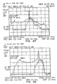
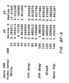
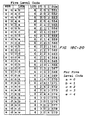
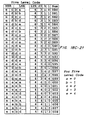
- FIGURE 8f shows a table and graph illustrating the error experienced by an envelope detector when data is in quadrature.
- Zero carrier occurs at 0 IRE units.
- White picture level occurs at 20 IRE units.
- 50% Gray occurs at 70 IRE units.
- 20% Gray occurs at 100 IRE units.
- Black occurs at 120 IRE Units and
- Sync tip level is at 160 IRE units.
- the column headings are for different levels of data with FIGURES 8b through 8e having been drawn for approximately 28 IRE units.
- the amount of error experienced by an envelope detector is computed and plotted in the FIGURE. As the data level increases, the degree of non-linearity also increases.
- the wave shaping circuits 895 of FIGURE 8a may be replaced with the new elements shown in FIGURE 9a. Because the data signal is digital, it can only have a finite number of kinds of interfering additions to the visual signal. Once these are determined, they may be stored as digital representations in Read Only Memory (“ROM”) and / or Random Access Memory (“RAM”) 9107 and recalled at the appropriate time and converted into an appropriate analog wave shape with Digital signal to Analog signal (“D/A”) converter 9109. The analog signal is then level adjusted in Level Controller 997 before being combined with the visual signal in Combiner 9103.
- ROM Read Only Memory
- RAM Random Access Memory
- D/A Digital signal to Analog signal
- the function of the Delay element 899 of FIGURE 8 can be more conveniently served in FIGURE 9a by the Digital Delay element 9111; however the analog delay of FIGURE 8a 899 would provide the required function equally well.
- the ROM/RAM Address Sequence Generator 9113 produces a correctly timed sequence of ROM addresses so that the ROM contents, after appropriate delay, may be converted to an analog signal and subtracted from the video. Depending on the signal and the types of receivers, the ROM/RAM 9107 contents may be changed. This can be accomplished by switching to a different set of data in the ROM or by augmenting the ROM with RAM which receives its contents by downloading from the point of origination of the data via RAM Data Download circuits 9115.
- concentrations of various classes of receivers' detectors may occur on a regional or national basis.
- concentrations of various classes of receivers' detectors may occur on a regional or national basis.
- the ability of these abatement systems to be selectively enacted permits their optimization on a regional basis.
- the population of various classes of receivers' detectors may change over time.
- FIGURE 9b shows a modification which can cause the abatement signal 9101 to be related to the Baseband Visual Source 901 output.
- the baseband video from the baseband visual source 901 is converted to digital form by Analog to Digital converter 9173.
- the digitized signal is delivered to ROM / RAM Address Sequence Generator 9113 which responds to this input and to the data from the Serial to Parallel converter 929.
- ROM / RAM Address Sequence Generator 9113 could be implemented in a number of ways.
- it can be a table of addresses which are arranged in rows and columns with one of the two inputs selecting a row while the other input selects a column.
- the address sequence then addresses appropriate locations in the ROM & RAM 9107 where the digital representation of the abatement signal is stored. The remainder of the system is as previously described in association with FIGURE 9a.
- FIGURE 9c shows an alternate approach.
- the abatement signal strength is varied in proportion to the visual signal. But the shape of the waveform is unchanged for various visual signal strengths.
- Level Control 997 is replaced with Level Control 997c which is electronically controlled by an input from transfer function unit 9175.
- Transfer unit 9175 takes its input from the output of Baseband Visual Source 901 and modifies it according to the way in which the amplitude of the Abatement Signal 9101 depends on visual level as described in FIGURE 8e and 8f.
- Transfer function unit 9175 can be implemented in a variety of ways. Non-linear networks using resistors and diodes can implement the transfer function.
- an analog to digital converter can be used to convert the video output of the Baseband Visual Source 901 to digital form. That digital signal can be used to look up values in a ROM or RAM look-up table which is then converted back to analog form with a digital to analog converter.
- the remaining challenge to implementing abatement is to determine the contents of the ROM and or RAM 9113.
- the abatement signal on line 9101 of FIGURE 9 and line 8101 of FIGURE 8a may be determined in a variety of ways.
- the signal may be calculated based on theoretical principles. Alternatively, it can be determined empirically.
- the broadcaster should be allowed to make his best estimate regarding the type and amount of signal shaping to introduce so as to minimize the total amount of artifacts seen by his audience.
- the determination of the abatement signals is performed separately and need not be in real time.
- the abatement signals may be dependent on the type of detectors in the receivers. If there are multiple classes of detectors in a marketplace, one strategy to minimize the impact of interference to the video may involve a compromise abatement waveform that may not be perfect for any one receiver, but will minimize the total impact on the population of receivers.
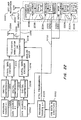
- FIGURE 10 illustrates the operation of several receivers 10117, 10119, 10121, and 10123 with differing detector types ranging from pure synchronous to pure envelope.
- the signal origination structure of FIGURE 7 generates a signal that will give rise to some small amounts of artifacts in the various receivers.
- the baseband visual signal is appropriately delayed in delay elements 10125, 10127, 10129, and 10131 and subtracted from the video outputs of the various receivers in Combiners 10133, 10135, 10137 and 10139. These processes generate the appropriate error signal for each receiver respectively on lines 10141, 10143, 10145, and 10147.
- the error signals are combined in proportion to the importance of the various detector classes in the local marketplace.
- the weight factor units 10149, 10151, 10153, and 10155 may have the same structures as the level controls of FIGURE 8a and 9a, 9b, and 9c and serve to proportion the error signals in accordance with the importance of their corresponding classes of detectors in the marketplace served by the system.
- a level control circuit may be implemented with a simple potentiometer or a sophisticated frequency compensated attenuator. These various abatement signals are combined in Combiner 10157. The result is the abatement signal found on line 10101 at the output of Combiner 10157. This output can either be used in its analog form or converted in Analog signal to Digital signal A/D, converter 10159. When converted to digital form, the information can then be used in the ROM and / or RAM 9109 of FIGURE 9a, 9b, and 9c.
- the television receivers 10117, 10119, 10121, and 10123 of FIGURE 10 may be replaced with just the relevant processing circuits and the resulting apparatus will be much more compact and less expensive.
- the relevant processing circuits of television receivers 10117, 10119, 10121, and 10123 may be simulated or modeled on a computer or other more convenient simulation of their effects.
- the weight factor elements 10149, 10151, 10153, and 10155 and the Combiner 10157 can be replaced with a computer program which searches for the optimum abatement signal.
- the structure of FIGURE 10 while suitable for the purpose, is more practically implemented in simulation.
- the abatement signal 10101 is a function of the baseband visual level. If a system which can only utilize an abatement signal which is independent of visual level is selected (such as FIGURE 9a), then FIGURE 10 is used with a desired baseband visual level. For example, a 20% gray level may be used to determine the abatement signal 10101 or its digital form coming from Analog to Digital converter 10159. If a system which can accommodate abatement signals which are a function of visual level is selected (such as FIGURE 9b or FIGURE 9c), then FIGURE 10 may be used with various visual levels at its input to obtain the analog abatement signal 10101 as a function of visual input level. Its digital equivalents are determined by Analog to Digital converter 10159.
- FIGURE 11 shows the system of FIGURE 10 in block 11163 generating an analog abatement signal 11101. Note that the block representing FIGURE 10, 11163, includes the system of FIGURE 7 in block 11165 for generating the signal with artifacts and the bank of receivers 10117, 10119, 10121, and 10123 of FIGURE 10 (or models or simulations of those receivers) which find the abatement signal 10101.
- the video and data are delayed an appropriate amount in Delay element 1 11167, and Delay element 11169 to compensate for the time needed to traverse the elements of the FIGURE 10 block 11163.
- These delayed signals are then fed into a second implementation of FIGURE 7 with the delayed baseband visual signal having first been combined with the analog abatement signal 11101 in Combiner 11171
- the power levels within the FIGURE 10 block 11163 in FIGURE 11 may be very low.
- the entire function may be modeled on a computer rather than being built in hardware.
- FIGURE 11 operates in real time, the abatement signals determined are a function of visual levels and are therefore optimized.
- FIGURE 12 shows the combination of FIGURE 8 and FIGURE 10 to generate the abatement signals in real time. No new elements are introduced and the elements retain their identification numbers from FIGURE 8 and FIGURE 10. Care must be taken to ensure the timing of all signals is correct. This is a feedback system and care must be taken to ensure stable operation and avoid oscillation. It may be necessary to reduce the data rate so that the propagation times of the various elements are not significant compared to the data waveforms. Alternatively, and possibly more practically, the system of FIGURE 12 can be modeled on a computer without the delays experienced in actual circuit elements. This implementation may operate at higher data speeds than would be experienced with a circuit implementation of these methods.
- FIGURE 12 operates in real time, the abatement signals determined are a function of visual levels and are therefore optimized.
- FIGURES 9b and 9c as well as FIGURE 11 and FIGURE 12 were shown to relate the amount of abatement signal to the visual level. Yet one more technique is described in FIGURE 13.
- the output of the video Amplitude Modulator 1303 is shown at 13179 and is presented to the negative input of Combiner 13183.
- the other input of Combiner 13183 comes from the 45.75 MHz Visual Reference Oscillator 1305.
- the output of the Combiner 13183 is shown at 13181 and is a double sideband modulated signal with the video modulation inverted from its normal mode. That is, sync tips are towards zero carrier as shown at 13179 rather than the other way (NTSC normal) as shown at 13181.
- This output 13181 is applied to one input of DSB modulator 13185.
- the data signal from the output of Digital to Analog converter 1331 is passed though LPF 1332 and waveform shaping circuits 1395 and is the unmodified abatement signal.
- DSB modulator 13185 may be thought of as a multiplier which multiples the abatement signal coming out of waveform shaping circuits 1395.
- the quadrature energy of the data signal exists in two phases with respect to the carrier at connection 1345. While the phases have the same magnitude, they are in opposite polarity. However, both phases serve to lengthen the resultant transmitted signal vector when combined with the modulated video carrier. Consequently, the abatement signal I' at the output of Delay & Phase Shifter 13189 must operate to reduce the output of combiner 1347 due to the data input signal Q.
- Waveform Shaping Circuits 1395 This is accomplished in Waveform Shaping Circuits 1395 by the use of two operational amplifiers, one developing the inverted output signal of the other.
- the output of each of the operational amplifiers is combined through steering diodes so that only one voltage state with respect to ground is present at the input of DSB Modulator 13185.
- These steering diodes function to form the mathematical absolute value function in the same manner as the diodes in a full-wave rectifier circuit as is well known to those of ordinary skill in the art.
- the rise and fall times of the abatement signal must follow the rise and fall times of the data encoder output Q at 1345 for the compensator to have optimal effect. It will be appreciated by those skilled in these arts that other circuits can be implemented which accomplish this same result.
- the maximum signal comes out of DSB modulator 13185.
- the minimum signal comes out of DSB Modulator 13185.
- the modified abatement signal is applied to Level Control 13187 and to Delay and Phase Shifter 13189 for precise adjustment before being subtracted from the sum of the modulated video plus the modulated data signals in Combiner 1347. Because the phase of the abatement signal I' is the same for each state of the quadrature data signal Q, the application of the abatement signal from the output of Delay & Phase Shifter 13189 is such that the I' signal always subtracts at combiner 1347. This reduces the contribution from the Pythagorean summation explained in Figures 8b through 8e.
- the waveform shaping circuits 1395 follow the principles previously described in relation to FIGURE 8a, block 895.
- the instantaneous solution of the Pythagorean Theorem (as described above in the discussion relating to FIGURE 8b through 8f) also results in a phase modulation of the visual carrier vector.
- transmission and reception certain signals are carried in sub-carrier form.
- An example of this would be the color information comprised of both burst and chroma signals.
- the chroma burst is time division multiplexed onto the synchronization signal. That is, a minimum of six and a maximum of nine cycles of the un-modulated color sub-carrier are switched into the synchronization pulse.
- the color signals are added to the NTSC monochromatic signal as a sub-carrier centered around a nominal baseband frequency of 3.58 MHz.
- the faithful reproduction of color information depends upon the preservation of a specific relationship between the phase of the burst signal and the sidebands representing the chroma encoding axes (nominally R-Y and B-Y).
- the inclusion of this information into the NTSC signal occurs through the production of two double sideband signals on quadrature sub-carriers at the 3.58 MHz frequency. If this carrier changes in phase or frequency, prior to the modulation process, the effect on the sidebands is inconsequential because they are still the product of the instantaneous frequency of the carrier and their baseband frequencies.
- a precise frequency and phase relationship is established for color detection at the beginning of each horizontal line. This is accomplished by locking a local oscillator in the receiver to the frequency and phase of a reference signal, called the chroma burst, transmitted at the beginning of each horizontal scan line. If a phase perturbation were to occur at the visual carrier frequency at a time after the burst but during the line controlled by that burst, the amount of that phase perturbation would be impressed upon the instantaneous phase of the chroma information by vector addition.
- the encoded data signal of the present invention is varying in symbol length and phase and amplitude (if more than two levels), in detectors which are susceptible to quadrature energy (such as the envelope type) the instantaneous resultant effect on the NTSC signal causes a phase modulation of the chroma information.
- This phase modulation is manifest as a displacement of the vectorial relationship of each component of color information present during the duration of the data symbol. This is a linear function in that the amount of phase shift introduced to the chroma signal is directly related to the data signal.
- Pre-distortion of the phase component of the NTSC color signal can be used to abate this problem and reduce it to essentially zero. At least one way that this may be accomplished is to perform independent correction to a part of the NTSC signal prior to its combining with the encoded visual data signal.
- a circuit termed a "Luma / Chroma Separator” 14191 may be constructed which separates the lower frequency luminance signal (that information below approximately 3.0 MHz) and the chroma information which operates essentially in the region 3.0 to slightly beyond 4.0 MHz.
- One such device is commercially available as "Video Enhancer Color Controller Pack" Model SD-E5 from Pioneer Electronic Corporation of Tokyo, Japan.
- circuit so that the burst information at 3.58 MHz and occurring only on the back porch of the synchronization signal is carried along the luminance path exclusively.
- the signal from the portion of the circuit carrying the luminance signal and burst 14193 is fed to the Amplitude Modulator 1403 as shown in the FIGURE 14.
- a signal from the Visual Reference Oscillator 1405 is fed to Amplitude Modulator 1403.
- a signal from the Visual Reference Oscillator 1405 is also adjusted in phase by Phase Shifter 14195 and amplitude by Level Control 14197 and applied to one port of a two port Combiner 14199.
- a signal from the Visual Reference Oscillator 1405 is also fed to Variable Gain Amplifier 14201 and applied to one port of a double balanced Mixer 14203 which is modulated with a logically inverted data signal which is inverted by Inverting Amplifier 14207 and supplied on line 14205. This is the logical compliment of the encoded data signal.
- the output of this double balanced Mixer 14203 is applied to the second input of Combiner 14199.
- the goal of these circuits is to produce the reciprocal of the impact of the encoded visual data signal to the signal generated by Amplitude Modulator 1403. This signal is then applied to a double balanced Mixer 14209 which is modulated with only the chroma signal on line 14211 separated from the composite signal in the circuitry 14191 previously mentioned.
- phase and amplitude of this double sideband signal is adjusted by Phase Shifter 14213 and Level Control 14215.
- the correct adjustment of Phase Shifter 14213 and Level Controller 14.4 14215 is so that the chroma information when combined with the output of Amplitude Modulator 1403 in Combiner 14219 is at the correct amplitude and phase so as to represent a faithful recreation of the original composite signal applied to the input of Luma / Chroma Separator 14191. This is first accomplished by adjusting the phase and amplitude of the chroma when no data is applied to line 14205 and the visual encoded data signal is off.
- This adjustment process reconciles the correct amplitude and phase for the chroma components when recombined with the luma / burst information derived by Luma / Chroma Separator 14191 and supplied to the Amplitude Modulator 1403.
- the output of double balanced Mixer 14209 must be filtered in Filter 14217 so that only the sidebands generated by the chroma signals are passed on to Combiner 14219. In a standard NTSC system this Filter 14217 will need to extract the region 41.57 MHz to 42.77 MHz and should display maximum attenuation at 45.75 MHz ⁇ 750 kHz.
- the circuitry of FIGURE 14 when correctly adjusted and operated can effectively reduce the phase perturbation introduced by the undesirable properties of an envelope detector on the color signal.
- a similarly constructed circuit could be developed which operated in the same manner upon the aural carrier of an NTSC television signal. When properly adjusted and operated, this circuit will remove the sympathetic phase modulation imparted by a certain class of detector on intercarrier sound signals. It is possible to build a single compensating circuitry operating over a spectrum sufficiently wide to encompass all of the aforementioned chroma region carried on line 14211 to doubly balanced Mixer 14209 in addition to the intercarrier aural frequency information (4.5 MHz in this example). In this example, not only would the adverse effects of certain classes of detectors on chroma be abated but also an artifact present in certain classes of aural detectors would be managed.
- Additional information may also be added on the aural carrier of the NTSC television format. This is achieved through amplitude modulation of the aural carrier which is already frequency modulated by the TV audio and BTSC signals.
- the first requirement is that the AM modulation may not be full depth without corrupting the aural program information.
- the allowable depth of modulation is limited by the worst signal to noise ratio to be encountered in the service area of the broadcasts.
- a downward modulation depth of about one half voltage (6 dB) which corresponds to 33% modulation is appropriate, but other values can be used.
- multilevel data signals may be employed increasing the data carrying capacity of the channel.
- multilevel means in this document more than one level and includes a two level signal as well as a signal with more than two levels.
- LBE Lower Band Edge
- the 8 level signal is less robust than an equivalent throughput realized in 4 levels.
- the FCC considered several proposals to incorporate embedded digital transmission within the NTSC spectrum.
- One of these proposals suggested that the upper side bands of the chroma signal could be cut off at 3.9 MHz above the visual carrier (+ 5.15 MHz LBE).
- the FCC heard this argument as well as objections to reducing the upper chroma bandwidth and decided to adopt the instant proposal and with it the reduction in upper chroma bandwidth.
- the 4 level, 1.5 Mb/s embodiment of the present invention was employed, it would be necessary to restrict the chroma upper sideband to 3.9 MHz above visual carrier. Under these conditions the 4 level signal would be 4.2 dB more robust than the 8 level example previously recited.
- the trade-off between an otherwise previously permitted encroachment on the chroma spectrum and a more robust signal can be decided by the implementer.
- a unique advantage of the signal of the present invention is its ability to be adaptive.
- AM modulated data signals In order to maintain pure amplitude modulation and thereby avoid producing interfering signals in the frequency/phase domain of the TV aural signal, the AM modulated data signals must remain symmetrical about the nominal carrier frequency within the band utilized by the FM aural information. This is accomplished by linear AM modulation.
- the FM modulated aural carrier is presented on terminal 15501 and the multilevel data from Multilevel Data source 15503 is to an AM Data Modulator 15505. This may be either conventional or downward (negative) modulation.
- the structure of AM Data Modulator 15505 may be any of those well known by those of ordinary skill in these arts.
- AM Data Modulator 15505 is preferably but not necessarily a linear amplitude modulator with some d.c.
- AM Data Modulator 15505 is followed by Band Pass Filter 15507 which constrains the signal to the FCC allowed spectrum and outputs a carrier with FM Aural information and AM data on terminal 15509.
- the output signal on terminal 15509 is then available for translation to the broadcast frequency, amplification, and radiation along with the visual carrier.
- An alternate approach to producing amplitude modulation of the data onto the FM aural signal is to separately generate the required sidebands and carrier components and add them to the FM aural signal.
- the data signal which is provided by the Multilevel Data Source 15503 is introduced to the AM Data Modulator 15505.
- the radio frequency port of this modulator is fed with a low level sample of the FM modulated aural signal available as set by control 15511. This sample is obtained from any convenient point in the transmitter aural signal path. Since amplification subsequent to AM modulation must be linear to preserve the AM information unaltered, this point is best chosen after the frequency translation and power amplification of the Sound Transmitter 1521 as shown in FIGURE 15b.
- the process of data modulation as in FIGURE 15a is performed.
- the resultant signal is adjusted in strength by control 15513 and directed to Comparator 15515 where aural program signal without the data modulation is subtracted from it providing a signal consisting of the additional components required for addition of the data.
- the resultant signal is filtered by Band Pass Filter 15507 to restrict the spectrum as previously explained and adjusted to the proper amplitude by control 15519 and then amplified by Amplifier 15521 and added to the aural program signal in Combiner 15523 producing the overall FM modulated aural signal with superimposed AM data modulation.
- the entire aural signal is then combined with the visual signal in Combiner 1511 in the conventional manner.
- steps can be implemented to truncate the upper sideband's signal so as to remain within the channel's bandwidth (6.0 MHz LBE or 4.75 MHz in the baseband). This can be accomplished with standard filtering. If a Surface Acoustic Wave Filter (“SAW”) or a digital signal processing technique is employed, it can minimize group delay. Or this can be implemented at baseband utilizing digital signal processing techniques while employing an I/Q modulator to establish the signal at the proper radio frequency.
- SAW Surface Acoustic Wave Filter
- the Band Pass Filters 15507 in FIGURES 15a and 15b truncate the upper sideband as well as limit the extent of the lower sideband as required.
- the difference frequency signal between the visual carrier and its companion aural carrier (4.5 MHz in the NTSC case) is recovered by the visual Detector 358, amplified, and limited by Limiter 364 prior to its application to the FM Detector 366.
- the BTSC aural channel has effective sideband products only up to ⁇ 120 kHz of 4.5 MHz of this channel, the necessary bandwidth of the existing 4.5 MHz circuitry is likely to be insufficient for aural data reception.
- the data signal of the present invention is AM, it will not survive transmission through a Limiter 364 stage. For these reasons, the aural data signal of the present invention, is best extracted from the television's IF amplifiers prior to any detection.
- a flat signal may be obtained by the use of a sharp high pass filter (at IF) which effectively removes the upper sideband energy in the RF transmitted spectrum. (See FIGURE 16a), 2) a filter with linear anti-symmetrical response that evenly tapers the upper and lower sideband energies resulting in a flat detected output (See FIGURE 16b), or 3) a baseband filter that reduces the lower baseband frequency amplitudes after demodulation (See FIGURE 16c).
- the Aural Sub-carrier including the AM data is presented to a High Pass Filter 16100a which converts the signal into a single sideband form.
- AM Detector 16102a is configured to detect single sideband signals.
- a Nyquist Filter 16100b equalizes the energy in both sidebands so that a AM detector 16102b can recover the aural data signal. This recovered signal when submitted to level comparator and clock recovery circuitry produces the aural data signal of the present invention at logical levels.
- a baseband equalizer 16100c is used instead of the filters 16100a and 16100b in the previous cases.
- a Baseband Equalizer accomplishes a filtering and / or phase adjustment function at baseband frequencies after demodulation. This function can be accomplished with analog or digital circuits, but digital techniques have become very cost effective and convenient to implement.
- the data capacity of the aural channel is a function of the bandwidth utilized, the efficiency of the modulation format employed, the minimum carrier to noise ratio to be encountered, and the degree of employment of error correction
- Bandwidth required is based on 20% data "excess bandwidth”.
- the TV chroma signal is protected from the data signal by filtering at the frequency listed as “lowest baseband frequency”. Some configurations are less practical (2 level and 16 level) and are less preferred.
- Carrier to Noise (4.08 MHz B/W) calculations are based upon 6 dB depth of modulation.
- the 36 dB C/N case considers aural carrier to be at -10 dB (broadcast mode) while at 43dB C/N (cable mode) - 15dB is used.
- 2 level data operates at basic S/N, 4 level is 7 dB worse and 8 & 16 levels degrade 6dB for each increase. The effects of vestigial filtering are not included.
- C/N 36 dB C/N(102dB/Hz) - Nyquist dBc - modulation depth - aural ⁇ Data
- S/N C/N - MLFAC (Multilevel Correction Factor)
- Figure 17a is a modification of the Conventional Television Receiver of Figure 3 to include the ability to recover the present invention's data.
- Directional Tap 1772 removes a portion of the signal energy flowing between the Mixer 1750 and the IF Amplifier with Nyquist Filter 1754 and presents it to the visual input of the Data Demodulators block 17110 on line 1778.
- the other input to the Data Demodulators block 17110 comes from a tap after the visual Detector 1758 and before the Limiter 1764 on line 1776.
- These signals are demodulated in Data Demodulators block 17110 and presented on lines 17112 and 17114 to the Data Extractors block 17116 which extracts the data and presents it on output lines 17118.
- the contents of the Data Demodulators block 17110 and the Data Extractors block 17116 will be described below.
- Figure 17b shows an alternate configuration of the receiver which allows the Optional Adaptive Equalizer 1756 to operate on the data visual signal.
- the IF Amplifier 1754 of Figure 17a is split into two parts.
- the first part 1754a does not include the Nyquist filter and so directional coupler 1772 may be connected after it so that the data is available on line 1778a for connection to the Data Demodulators block 17110.
- a directional coupler is a device for separating a portion of the signal energy and providing it on a tap output to some circuits while providing the remaining signal energy to following circuits on the other output which is called a pass-through output.
- a directional coupler The objective of a directional coupler is to maintain signal isolation between its input and its outputs so that strong signals to not back feed to circuits not intended to receive them.
- the directional coupler 1774 may be used instead after the signal goes through the Optional Adaptive Equalizer 1756.
- the splitting of the IF amplifier for these purposes is not to be confused with the split sound technique described earlier as a method of television receiver design.) This has the benefit of allowing the Optional Adaptive Equalizer 1756 to compensate for transmission path deficiencies.
- the second part of the IF amplifier 1754b includes the receiver's Nyquist filter.
- a separate ghost canceller may be employed for the data signal.
- FIG 17c shows the details of the Data Demodulators block 17110.
- Band Pass Filter (BPF) 1780 restricts the energy to those frequencies which carry the present invention's data. Note that the bandwidth of BPF 1780 goes slightly beyond the 750 kHz double sideband region of the NTSC signal. Because of this, it includes part of the visual spectrum which will cause some degradation of the received data. This is not considered significant. However, abatement techniques similar to those utilized in other parts of the present invention can be added if desired.
- the design of Band Pass Filter BPF 1780 is well known to those of ordinary skill in these arts and can be implemented using software packages previously cited. The signal from the BPF 1780 then travels two paths. The first path takes it to Phase Locked Loop 1784.
- Phase Locked Loop 1784 produces a stable cosine wave of the same frequency and phase as the visual carrier.
- Phase Locked Loop 1784 may be implemented with a wide variety of integrated circuits or using discrete semiconductors. Just one suitable example is the TLC3923 chip by Texas Instruments which serves this purpose when operated in the manner intended by its manufacturer.
- Phase Shifter 1786 shifts the phase of the output of Phase Locked Loop 1784 so that it is in quadrature with the visual carrier and therefore in phase with the present invention's visual data signal.
- Phase Shifter 1786 may be implemented with the Mini-Circuits PSCQ2-50 previously cited.
- the second path from the BPF 1780 leads first to Amplifier 1782 which provides appropriate signal strength to drive double balanced Mixer 1788 where the cosine wave from Phase Shifter 1786 is also made available.
- the Mini-Circuits SRA-1 is commercially available and is a suitable mixer for this purpose. Since the phase of the output of the Phase Locked Loop 1784 has been adjusted by Phase Shifter 1786 to be in phase with the quadrature data signal, Mixer 1788 can recover that signal.
- the output of Mixer 1788 is, in the general case, a multilevel signal. It is simultaneously fed to a Clock Recovery circuit 1792v which recovers the timing information from the multilevel signal.
- Clock Recovery circuit 1792v can be implemented in many ways. Just one example is the Elonics EL2019 clock recovery integrated circuit.
- the clock signal times Level Slicer 1794v and Parallel data to Serial data converter P / S 1796v.
- the Level Slicer 1794v determines when threshold values are exceeded by the multilevel signal from Mixer 1788 and therefore what logic values are estimated to be received. When more than two levels are encoded simultaneously, more than one logic bit is sent simultaneously.
- the Parallel data to Serial data converter P / S 1796v puts the data in serial form to be presented to the user on terminal 1798v. Alternatively, the data is presented to Data Multiplexer / Demultiplexer 17106. More will be said about Data Multiplexer / Demultiplexer 17106 below.
- FIGURE 16a and FIGURE 16b discussed two possible forms for the Data Filter 17100.
- FIGURE 16c a third configuration was described in FIGURE 16c. If that configuration is implemented, AM Detector 17102 is placed ahead of Data Filter 17100 and Data Filter 17100 is realized using digital filter techniques.
- Clock Recovery circuit 1792a serves the same function and can be implemented in the same manner as Clock Recovery circuit 1792v.
- Level Slicer circuit 1794a serves the same function and can be implemented in the same manner as Level Slicer circuit 1794v.
- Parallel data to Serial data converter P / S 1796a serves the same function and can be implemented in the same manner as Parallel data to Serial data converter P / S 1796v.
- the Parallel data to Serial data converter P / S 1796a puts the data in serial form to be presented to the user on terminal 1798a. Alternatively, the data is presented to Data Multiplexer / Demultiplexer 17106.
- Data Multiplexer /Demultiplexer 17106 is optional and can used to assemble data from the aural sub-carrier and the visual carrier into a larger data stream. It will be clear to those skilled in these arts that the other methods of data carriage in analog signals can also be used in conjunction with these inventions. Thus, while not shown in FIGURE 17a, data carried in the Vertical Blanking Interval, in systems devised by others such as Digideck and WavePhore, and in other sub-channels may be combined without further invention to provide a higher data capacity. Conversely, the data conveyed in the aural channel and the data conveyed in the visual channels may be subdivided into lower capacity data streams for purposes which are not demanding of the full capacity of these channels. These multiplexing and demultiplexing techniques are commonly used and understood in these arts and require no further explanation.
- connection 17104 provides the clock signal to the path which does not have its own Clock Recovery block.
- FIGURE 17d shows an improved demodulation circuit for the visual path of the present invention.
- the Band Pass Filter 1780 is avoided because of its potential to disturb the phase of the data signal and contribute to demodulation errors. Instead, part of the output of Amplifier 1782 on line 17124 feeds Mixer 17122 whose other input comes on line 17120 from the non-phase shifted output of Phase Locked Loop 1784. Thus the output of the Mixer 17122 on line 17126 is the synchronously detected baseband visual signal.
- High Pass Filter 17128 aggressively removes the portion of the video which is in the same band as the data signal. The remaining signal is that which would interferes with data detection. It is conveyed on line 17130 to the subtracting input of combiner 17132. The other input to the combiner 17132 comes from the Mixer 1788 on line 17134.
- the data signal with the interfering visual signal removed is presented on line 17112 to the Data Extractor block 17116 of FIGURE 17c.
- FIGURE 17e is an implementation of a data receiver which is separate from a television receiver.
- the visual and aural signals are not detected and used for their normal purposes.
- FIGURE 17e will be recognized as FIGURE 17b with the following elements deleted: Sound Reproducer 1770, Audio Amplifier 1768, FM Detector 1766, Limiter 1764, Video Processor 1760, and Video Display Device 1762.
- Detector 1758 survives in abridged form. Its sole function is to serve as a non-linear device to bring the aural sub-carrier which contains AM data down to baseband frequencies for conveyance on lines 1776 to the Data Demodulators in 17110.
- Such a device can be built into a much smaller and lower cost set top box or other small cabinet since it does not have the picture and sound producing devices and their expensive and power consuming components.
- Binary signals are transmitted in succession and grouped together to form binary words. Traditionally, eight bits are called a byte. Occasionally, four bits are called a nibble. The number of bits which form a "binary word" depend on the design of the equipment processing the data. When data is transmitted, it is usually organized into bytes.
- FIGURE 18a shows the familiar two level binary code considered to this point.
- the order of the bits are defined to progress from Least Significant Bit (LSB) to Most Significant Bit (MSB) and the location in the stream is assigned a value or weight.
- the weights in the binary system are as below.
- the binary system has just two symbols: 0 & 1 while the decimal system has ten symbols: 0, 1, 2, 3, 4, 5, 6, 7, 8, and 9.
- the transmission path can support more than two levels, it is customary to attempt to utilize levels which are a power of two and to consider multiple bits to be simultaneously transmitted. So for example, if four levels can be transmitted, they can define two simultaneous bits:
- the eight levels can define three simultaneous bits:
- the transmission path can support ten levels, it is possible to do something quite different.
- the levels can directly represent the decimal system:
- FIGURE 18a show how to proceed.
- the familiar Two Level Code is shown on the left for the transmission of four bits with the MSB on the left and the LSB on the right.
- the "weight" of each position is indicated.
- the "Sum” column is formed by taking each the columns contents and multiplying it by that column's weight and totaling the values for the row.
- the three level code fills the center and right columns and it is created in the same manner.
- three are utilized: a, b, and c.
- the tables of FIGURE 18c show how to proceed. At the top of the columns, the "weight" of each position is indicated.
- the “Sum” column is formed by taking each the columns contents and multiplying it by that column's weight and totaling the values for the row.
- five are utilized: a, b, c, d and e.
- the present invention provides for apparatus, systems and methods of expanding the throughput capability of the Vertical Blanking Interval (VBI) by the inclusion of multiple signal levels of more than two levels (The term "multilevel" means in this document more than one level and includes a two level signal as well as a signal with more than two levels.) in a manner nominally otherwise consistent with current Teletext and VBI practice.
- the application of Teletext signals within the scope of the current art places a logical one and logical zero at levels which equate to 0 IRE and 80 IRE respectively.
- the current state of the art in television receivers includes ghost canceling circuits, some designs based upon the Ghost Canceling Reference (GCR) signals. These techniques mitigate the impact of ghosting on television reception.
- Cable television systems are generally operated in such a way so as to be materially free of ghosting. In both the foregoing examples sufficient performance margin exists to permit the successful adoption of multilevel data of more than two states and thereby the increase of data throughput over a two level system.
- current Teletext signals convey thirty-two eight bit words in each VBI line allocated or 7,680 b/s per VBI line in each field. While there are twenty-one lines in the VBI, nine are required for the vertical synchronization signal and one is reserved by the FCC for the Closed Captioning signal. This leaves eleven lines every sixtieth of a second or a bit rate of 168,960 b/s. If eight level signaling is employed, this triples to 506,880 b/s. It will be appreciated that since the digital television system uses 8-VSB and 16-VSB modulation, it is not unreasonable to consider higher number of levels such as 16. This would convey four simultaneous bits or 675,840 b/s.
- the circuitry to implement these approaches is a combination of standard teletext decoder clock recovery and an enhanced level slicer which can discriminate the number of levels chosen.
- the level slicer is the same as found in FIGURE 17 of the present invention.
- FIGURE 19a shows the manner in which a Digital signal to Analog signal converter can be implemented. There are a wide variety of methods of accomplishing this function and a plethora of commercially available integrated circuits which can be used for this purpose.
- FIGURE 19a illustrates one implementation of a two bit system and is for illustrative purposes only without limiting the choices of actual implementation.
- the MSB data input D 1 1902 and the LSB data input D 2 1904 result in output voltage V 0 1908 from D / A converter 1906.
- a common method of implementation familiar to those skilled in these arts involves the use of controlled current sources of unequal magnitude feeding a resistor.
- the MSB current source I D1 1910 has twice the strength of the LSB current source I D2 1920.
- output voltage V 0 1908 will be one volt for each unit of current from current source I D2 1920 and two volts for each unit of current from current source I D1 1910 as shown below: D 1 D 2 MSB LSB V 0 off off 0 0 0v off on 0 1 1v on off 1 0 2v on on 1 1 3v
- FIGURE 19b shows one implementation of a slicer circuit using a differential amplifier technique familiar to those skilled in these arts. There are a wide variety of methods of accomplishing this function and a plethora of commercially available integrated circuits which can be used for this purpose.
- FIGURE 19b illustrates one implementation and is for illustrative purposes only without limiting the choices of actual implementation.
- the differential amplifier can be used as a slicer to determine if an input voltage is above or below a threshold voltage.
- FIGURE 19b configures three slicers 1952, 1954, and 1956 of the type shown on the left side of FIGURE 19b to determine if the input voltage V in 1940 exceeds threshold voltage V th1 1958, threshold voltage V th2 1960, or threshold voltage V th3 1962 formed by a resistor ladder consisting of resistors R1 1964, R2 1966, R3 1968, and R4 1970.
- V th1 1934 and 1958, V th2 1036 and 1960, and V th3 1038 and 1962 are set at 0.5 volts, 1.5 volts, and 2.5 volts respectively.
- the outputs of the three level slicers 1952, 1954, and 1956 are as follows: Logic Inputs MSB, LSB 00 01 10 11 Input Voltage 0v 1v 2v 3v Slicer # 1 L H H H Slicer # 2 L L H H Slicer # 3 L L L H
- the "L” in the above table indicates a lower voltage or a logic 0 while the "H” indicates a higher voltage or a logic 1. It can be seen that Slicer #2 1954 directly indicates the value of the MSB.
- the LSB is at logic one when Slicer #3 1956 has a high output or when the combination of Slicer #1 1952 has a high output and Slicer #2 1954 has a low output. This logic is realized in Logic Block 1972 with logic Inverter 1974, And Gate 1976, and Or Gate 1978.
- FIGURE 19c describes the use of unequal steps in the encoding of data to provide differential noise immunity and differential immunity to distortion, and interference to two data signals.
- the MSB current source I D1 has been chosen for illustrative purposes and not as a limitation to be three times the strength of the LSB current source I D2 . This causes the center step riser to be twice as large as the other two step risers and gives the MSB twice the noise immunity as the LSB.
- the threshold voltages are adjusted as indicated and the MSB carries more important data than the LSB.
- the MSB remains recoverable after the noise, distortion, or interference causes the LSB to be unrecoverable.
- the differential in immunity may be selected to be any appropriate value for the specific application.
- Future television receivers can take advantage of the availability of the abatement signal to adjust the abatement signal for their particular structure.
- a fully synchronous receiver would not need the abatement signal and actually would suffer by some small amount from its imposition. Because the inherent performance of the fully synchronous detector is at an initial high level, the slight contribution of the abatement signal in an adverse way to this class of detector is not consequential.
- the data that is used in the transmitter's ROM /RAM 9113 can be made available to the receiver in the digital data stream.
- it can be converted to an analog waveform, correctly timed, modulated onto an appropriate IF frequency and subtracted from the received signal. If the receiver's detector needs no abatement, the signal is restored to its original condition. If the receiver's detector requires a different kind of abatement, it can be constructed locally within the receiver correctly timed, modulated onto an appropriate IF frequency and added to the signal before video detection.
- FIGURE 20 shows apparatus, systems, and methods for doing this.
- a Local Oscillator 2002 at an appropriate frequency supplies Mixer 2004 with one of its inputs.
- the other input to Mixer 2004 is a modulated television signal.
- the output of Mixer 2004 is at an IF frequency.
- the signal is conveyed to a Visual IF Amplifier 2010 which passes and amplifies only the visual portion of the signal.
- Directional Coupler 2008 separates a portion of the signal and conveys it to Aural IF Amplifier 2012 which passes and amplifies only the aural portion of the signal.
- Directional Coupler 2006 separates a portion of the signal and conveys it to Phase Locked Loop (PLL) 2014 which provides an un-modulated output carrier on lead 2016 which is locked in phase and frequency to the visual carrier.
- PLL 2014 Phase Locked Loop
- the output of PLL 2014 is phase shifted by an appropriate amount in Phase Shifter 2018 so that the optionally suppressed data carrier is in quadrature with the visual carrier. This is similar to 525 of FIGURE 5A (or any of the other implementations of the Data Encoder of the present invention).
- the output of the Data Encoder 20525 is provided to Combiner 2020.
- the output of Data Encoder 20525 is optionally also provided to Abatement Signal Generator 20995 similar to the Abatement Signal Generator of FIGURE 9b (or any of the other implementations of abatement signal generators of the present invention) which generates an appropriate baseband abatement signal. If the methods of FIGURE 13 are used to generate the abatement signal, Optional Abatement Signal Generator 20995 will also requires an input from Visual IF Amplifier 2010 and Phase Lock Loop 2014. The output of optional Abatement Signal Generator 20995 is provided to AM Modulator 2022, the other input of which comes from PLL 2014. The output of the AM Modulator 2022 also goes to Combiner 2020. The combined output of Combiner 2020 is a visual television signal with quadrature data and optional abatement signals. It will be appreciated that the methods of FIGURE 4 and FIGURE 6 could also be employed to add visual signal data.
- the aural carrier data is processed in Aural Data Generator 2024 and modulated onto the aural carrier in Aural Data Modulator 2026.
- the output of the Aural Data Modulator 2026 is combined with the visual signal in Combiner 2028.
- Mixer 2030 is supplied with the output of Local Oscillator 2002 and heterodynes the combined signal output of Combiner 2028 back to its original frequency.
- Band Pass Filter (BPF) 2032 restricts the signal to its assigned frequency band and amplifier 2034 brings it to the appropriate strength for the purposes intended. It will be appreciated that subsequent frequency translation can be applied through the implementation taught in FIGURE 20 so as to place the NTSC signal encoded with data as provided in the present invention onto a different frequency.
- An important aspect of the present invention is its scaleability to accommodate differing transmission path conditions as well as various application data rate requirements and economic constraints. Scaleability comes from two factors. Firstly, there is the ability to utilize three different paths for data transmission: the visual carrier, the aural carrier, and the VBI. Secondly, each of the paths can employ multiple signal levels ranging from two level binary to multiple levels in powers of two and even to multiple levels which are not powers of two. These various resources can be multiplexed into higher data capacity paths or demultiplexed into many smaller scale paths. The resources from multiple 6 MHz channels and FM signals can be multiplexed for still higher data rates.
- Some of the data paths of the present invention will be more robust than others. Some of the data paths of the present invention will be more costly to implement than others. The wide range of capability and scalability accommodates many marketplace needs.
- the communications infrastructure is becoming increasingly more complex.
- an indicating light was typically displayed on receivers to indicate the signal was present.
- signals not directly related to the programming material such as some of those envisioned by the apparatus, systems, and methods of the present invention, it would be useful and convenient, to survey the resources of a channel and to a larger extent, all of the channels, within the range of an off-the-air receiver or provided over a cable or similar television delivery system.
- This assemblage of information should be carried along with the aggregate of services and be made readily available so that operators of / or receivers of these services can conveniently determine which resources are being utilized.
- At least one implementation of this directory system is the use of a teletext-like code on a VBI line, for example, line 20. This code could be implemented as binary or as multi-level. A progressively added set of data words would be inserted to allow those who operate on the signal to leave their identifications on it.
- the directory can optionally contain information defining the source of various data, the purpose of the data, the structure of the data, and its location. The last piece of information is important because the data may be a subset of one of the data paths or it may be a combination of multiple paths in one 6 MHz channel or even spanning multiple 6 MHz channels.
- the location data provides the instructions necessary for the local demultiplexer or multiplexer to find and separate out the desired data streams.
- a PIN Diode modulator is interposed in such a way as to reduce the amplitude (thus creating a digital bit) of the previously black video signal during the prescribed portion of the line.
- the reduction of black in the RF domain results in a shift upward in IRE level to a state nearer white (100 IRE) thereby creating a logical one.
- the first user of a resource asserts his presence by producing a word through the use of the PN Modulator stating who is using what resource through a brief prearranged code.
- a subsequent user of a resource first examines the progressive word already written to see if the desired resource is available and adds his information immediately adjacent to the occupied portion of the line.
- the described technique permits imposing data onto the specified line without demodulation and remodulation of the affected signal.
- the information asserting the condition of the resource's use can be returned to a black or near black state indicating once again the availability of the resource in the channel.
- Most current production televisions offered for sale within the US have decoding circuits which recover Closed Captioning signals transmitted within the VBI.
- Receivers of the progressive word can be patterned along these designs and this feature may be an extension of their functionality.
- the present invention avails itself of the affordable complex signal processing developed since the advent of television and applies this processing to more effective use of the television and radio spectrum.
- the present invention discloses apparatus, systems, and methods which permit the inclusion of many megabits per second of digital data compatibly within a television signal.
- This data resource can be used for multiple purposes including conveying several television programs with stereo (or surround) sound or providing data to computing, information processing, or display devices.
- the data capacity may be simultaneously split between these applications.
- the data capacity will be used in total or in part for enhancement signals which improve the quality of the analog channel or to provide information relevant to the programming carried on the analog channel.
- the portion allocated to one application versus any other may vary with location or vary with time at a given location. Some Internet applications will see speed improvements of nearly a hundred times. All of this capability happens compatibly with existing Broadcast and Cable facilities and is very cost effective.
- the present invention sets forth apparatus, systems and methods for applying data within the spectrum occupied by: 1) the visual carrier (that radio frequency carrier onto which the video information signal is applied), 2) aural carrier (that radio frequency carrier onto which the aural information signal is applied), and 3) the VBI.
- the present invention also provides a communications pathway for identifying the allocation of these data resources.
- the present invention enables the transmission (over the air and within cable) of additional programming and data resources which are expected to be well received by viewers. These programs and services go where ever the hosting television signal goes and may be delivered selectively to subscribing viewers by conditional access techniques or supplied for the reception of anyone possessing the necessary receiving equipment.
- the present state of the art in digital video compression is based on the Moving Pictures Experts Group (MPEG) digital video compression standard.
- MPEG Moving Pictures Experts Group
- a current implementation of this invention provides for the transmission of approximately 4.5 Mb/s of data in the television signal.
- the use of multi-level signaling in the VBI could add another half Megabit per second to this number. This resource could be used for the provision of three complete MPEG television signals while simultaneously transmitting an analog television signal for use with existing receivers. This dramatic improvement in spectral efficiency is not found in the prior art.
- the present invention enables the generation of additional program channels without bandwidth expansion. That is, the need for physical upgrading of the cable system is avoided. Moreover, the cable television head end cost to implement the present invention is modest and fully supported by the benefits. The special equipment of the present invention will only be installed in the homes taking the new services and providing corresponding new revenues.
- the present invention can be added to over the air broadcast television providing additional viewing choices and solving the capacity limitations of the prior broadcasting art.
- Multilingual programming can be expanded into communities where such needs are unmet or under-served.
- TV receiver prior art has technical limits which preclude the addition of more stations. Many television receivers cannot separate adjacent channels of disparate strengths. Many television receiver tuners have insufficient image carrier rejection. They will allow response to channels that are located in frequency on the opposite side of the Local Oscillator frequency from the intended signal. This undesired response is found displaced from the Local Oscillator frequency by an amount equal to the IF frequency. Other tuners have non linear characteristics that respond to harmonics or subharmonics of the tuned frequency. The use of a single channel in a market may preclude the use of up to seven otherwise useable frequency assignments for other purposes. These constraints are considered by the FCC in the adoption of its Table of Assignments, better know as the television channel taboos.
- the present invention enables more programming to be compatibly and simultaneously carried with the existing analog television signal in the same spectrum.
- FIGURE 21 shows three Program Sources 2102, 2104 and 2106 which include video and audio presented to three Digital Compression units 2108, 2110 and 2112.
- Digital Compression units 2108, 2110 and 2112 could, for example, be implemented with the MPEG standard.
- a wide variety of MPEG digital encoding equipment is available commercially ranging from add-in cards for personal computers costing a few hundred dollars to extensive processors costing hundreds of thousands of dollars.
- An MPEG1 encoder card (called the Broadway Card) for use in PCs is available for $799 from the Data Translation corporation, Broadway Group of Marlboro MA. (800-249-1000). Quite acceptable results are obtainable at data rates of 1.5 Mb/s.
- FIGURE 21 utilizes the present invention's four level signaling implementation of the visual carrier as previously described in Visual Data Encoder 2114 yielding a 3.0 Mb/s capacity which can carry two 1.5 Mb/s signals.
- the aural carrier methods of the present invention as previously described are illustrated in FIGURE 21 as Aural Data Encoder 2116.
- the Aural Data Encoder 2116 can carry an additional 1.5 Mb/s digital video signal.
- These signals are combined in Television modulator or Transmitter 2118 with an analog video signal from the Program Source #4 2120.
- Television modulator or Transmitter 2118 is a low power modulator whose output is combined with the outputs of other low power modulators and put down a combination of fiber and coaxial cable 2140 for delivery to subscribers.
- Program Source # 4 2120 includes means for inserting the signal from the VBI Data and the Directory generator 2122 of the present invention. This information is applied to the analog input of Television Modulator or Transmitter 2118. All of the components of these elements are previously described as part of the present invention.
- signals from the sources are conveyed over cable 2140, MMDS microwave antenna 2142 or Off-Air Reception Antenna 2144.
- the received signals pass to an ordinary existing analog television receiver TV # 1 2124 with remote control 2126
- Television Receiver 2124 receives and utilizes the analog NTSC portion of the signal in the usual manner.
- receiving circuits in Decoders 2130, 2134, and 2138 operating according to the present invention as described previously extract three additional digital programs and convert them to NTSC signals for ordinary television receivers TV # 2 2128, TV # 3 2132, and TV # 4 2136.
- These ordinary TV receivers may also optionally be VCRs, have VCRs built into them or have VCRs used with them. It will also be appreciated to those skilled in these arts that the output signals of decoders 2130, 2134, and 2138 could be connected to alternative display devices such as those associated with personal computers.
- FIGURE 22 shows a particularly advantageous application of the present invention.
- a Decoder according to the present invention is built into DVD / Decoder unit 2238 which is connected to ordinary TV # 3 2136.
- the Digital Video Disk also called the Digital Versatile Disk because of its ability to serve as a high-capacity replacement for the CD-ROM
- the Digital Video Disk is a commercially available product with great promise but some consumer resistance due to its current inability to record.
- As a play-back-only device for pre-recorded media it has limited appeal. It is also modestly expensive since it includes decoding circuits and memory for MPEG processing.
- the addition of the data transport apparatus, systems, and methods of the present invention to the DVD player greatly expands its utility and value.
- the Internet and similar data services are constrained by limited transmission capacity of the prior art.
- data may be received which is intended only for the recipient much like a private telephone conversation or a personal letter.
- the recipient may have a desire to receive information, which while specialized, is of interest to multiple recipients.
- the user of the Internet or other similar service may wish to search a large data base through key-words for information on or about a specific topic. The way that these data are requested and received is quite different.
- the present invention also addresses the ever expanding need for data into homes and offices.
- Much of the data service provided today is of a highly asymmetrical nature. That is, where a simple request of a few hundred bytes generated by a user of the Internet or similar services results in the downloading of a much larger file.
- These Internet and Internet-like needs when served over telephone networks result in the downstream information being severely constrained by the capacity of the phone network.
- This constraint is limited by the physics of the network as studied by information theorists such as Claude Shannon and others. That is, it is limited by the laws of Physics and is not going to increase.
- the present invention substitutes apparatus, systems, and methods which have not reached similar limits and thereby enables much more satisfactory service.
- the recipient can solicit information on a subject through the selection of key words or similar identifiers which permit their receiver to extract the desired information out of the circulating data stream(s). Additionally, the information can be organized into "magazines", “chapters”, and “pages” which are listed in a system of indices. The recipient of the information indicates which of these are of interest and they are captured and stored locally. This is referred to as "Push Technology". Unless the amount of information is very large and circulation very rapid, its practical value is limited as was the case of Teletext. As we move to an information based society, it is expected that Push Technology either standing alone or in conjunction with other programming sources such as radio and television will be broadly utilized. The present invention enables Push Technology over broadcast and cable to an extent here to fore not envisioned by prior art methods.
- the viewer of a television program may move a cursor on the screen over an object and "click" on it using a wired or wireless remote control. This action could link the viewer to additional information on the object designated. That information may be historical, encyclopedic, or for purchasing. Other Web sites may be automatically accessed. If for illustrative purposes, the viewer designated an article of clothing, he may choose color, style, size, method of delivery and make a payment choice. These actions may be implemented in a small sub-area of the picture and allow the program to continue without interruption. It will be appreciated that while these sorts of actions were possible with still pictures and graphics in some versions of the prior art, data capacity and speed limitations made it impossible to apply these techniques to moving pictures of ordinary television programming. The present invention affords very high speed capacity which will enable such advanced services.
- FIGURE 22 shows the situation of FIGURE 21 with one or more of the Program Sources 2102, 2104, and 2106 of FIGURE 21 replaced by Data Sources 2202 and 2204.
- Digital Compression units 2208 and 2210 reduce data redundancy and save transmission time.
- any or all of the Program Sources 2102, 2104, and 2106 of FIGURE 21 can be replaced with Data Sources. In this illustration, only two were replaced and one digitally compressed program was maintained.
- the Program Sources and the Data Sources can be utilized with any of the data transmission resources of the present invention.
- On the receive side one or more of the TVs or VCRs are replaced with personal computers or information retrieval and display devices. Ordinary television receiver TV # 1 2226 continues to utilize the normal analog NTSC transmission.
- Ordinary Television Receiver 2228 is connected to Web Appliance receiver 2230 which converts the data received into appropriate screens for display on ordinary Television Receiver 2228.
- the Web Appliance receiver 2230 does not have to include an MPEG decoder. It does however convert the received data and Web Pages into suitable form for conveyance to the ordinary Television Receiver 2228.
- the Web Appliance receiver can also access e-mail and other Web services if it is provided with a return path to the Data Sources 2202 and / or 2204.
- the return path needs only be of sufficient capacity to convey key strokes back to the signal source.
- a twisted pair dial-up land-line 2250 may be used. If the cable system 2240 has two-way capability, it can be used for the return path.
- Microwave antenna 2242 may also be used for return path signals at some time in the future as that technology continues to evolve.
- Decoder 2234 serves Personal Computer PC # 1 2232.
- PC # 1 2232 includes a conventional computer keyboard designated as "qwerty" in FIGURE 22 and the usual computer peripherals. Decoder 2234 may simply convey data to PC # 1 2232 or may also display video. In the latter case it may include an MPEG decoder. Alternatively, the MPEG process may be implemented in PC # 1 2232 as hardware and / or software.
- Figure 23 shows how television channels can be combined to carry greater capacity than any one channel can carry.
- Program Source # 1 2306 provides signals to Digital Compression unit 2312 and
- Program Source # 2 2304 provides signals to Digital Compression unit 2310 and
- Program Source # n 2302 provides signals to Digital Compression unit 2308.
- "n" is an arbitrary number. A large number of Program Sources and Digital Compression units can be assembled yielding a need for a high data capacity in the transmission channel.
- Data Source 2340 provides data to Digital Compression unit 2342.
- Statistical Multiplexer 2314 merges the data streams into one based on the statistics of usage of these various sources. The use of Statistical Multiplexing allows more data to be carried since Program Sources and Data Sources which at a given moment have need for only a small capacity can relinquish excess capacity to Program Sources and / or Data Sources which urgently need it.
- the data stream from Statistical Multiplexer 2114 may exceed the capacity of one channel's Visual Data Encoder 2320, Aural Data Encoder 2322, or VBI Data stream 2324 Then, that channel's Television modulator or Transmitter 2328 will be over loaded.
- Data Distributor 2316 presents the data to multiple channels 2318a, 2318b, and 2318n. This is done in a manner so that any signal from one Program Source or one Data Source goes to two or more adjacent channels. These channels are summed in Combiner 2334 before conveyance by cable 2338, MMDS microwave antenna 2336, or over-air transmission by the separate antennas of the multiple Television modulator or Transmitter systems. Note that a single-channel version of MMDs exists, Multipoint Distribution Service (MDS).
- MDS Multipoint Distribution Service
- FIGURE 23 draws the tuner explicitly to emphasize the application.
- Tuner # 1 2350 services Decoder 2352 which extracts the data in the channel tuned by Tuner # 1 2350 and conveys it to Multiplexer 2354.
- Tuner # 2 2356 services Decoder 2358 which extracts the data in the channel tuned by Tuner # 2 2356 and conveys it to Multiplexer 2354.
- Tuner # n 2360 services Decoder 2362 which extracts the data in the channel tuned by Tuner # n 2360 and conveys it to Multiplexer 2354.
- Multiplexer 2354 assembles the data from the "n" channels and presents it for use to appropriate devices such as PC # 1 2332 in FIGURE 23.
- PC # 1 2332 in FIGURE 23 is merely an example of a device which can utilize high speed, high capacity data streams. As shown in FIGURE 22, PC # 1 2332 in FIGURE 23 may have a return path for interactive applications.
- the Statistical Multiplexer 2314 increases the efficiency of the utilization of the data carrying resource by allowing Program Sources which have much detail and / or motion to temporarily utilize more of the available data capacity while Program Sources which have little detail and / or motion to temporarily contribute capacity to other needs. Since this is based on statistical phenomena, the more Program Sources involved, the more efficient will be the result. This results in the data from some Program Sources to be distributed to more than one channel. Consequently, a receiver may need to monitor more than one channel to extract the information necessary to re-create the Program Source data stream. Because of this Multiplexer 2354 is used to assemble a data stream which is delivered to MPEG Decoder 2366 to service television receiver TV #1 2368.
- Data Distributor 2316 is operated in a manner that insures that data from any one Program Source will usually be found on no more than two channels. These channels do not have to be adjacent and they can be reassigned from time to time. The VBI Directory can assist in making these assignments.
- FIGURE 24 is similar to FIGURE 23 in most respects with the following differences.
- Higher Resolution Program Source 2402 provides higher performance television signals such as, for example, the Advanced Television Systems Committee standard signal formats approved by the FCC in December of 1997. These range from multiple SDTV signals to HDTV signals requiring up to 19 Mb/s. Other formats are equally acceptable. A capacity of 19 Mb/s would require the utilization of two or more channels.
- Multiplexer 2454 services advanced digital television receiver TV 2468.
- TV 2468 may optionally include a wide screen, higher vertical and horizontal resolution, 5.1 channels of surround sound, progressive scan, wider color bandwidth displays and multiple languages in both sound and captioning.
- the present invention also enables the delivery of signals which may be used for the enhancement of quality of the hosting analog television channel.
- These enhancements include but are not limited to digital sound (current NTSC television sound is analog), improved color signals and other signals which will allow for a higher quality analog signal to be seen on advanced television receivers.
- This functionality can also include information regarding the program being displayed. This information might include the name of the program, the time remaining in a movie, or the call letters of a station or name of the programming service.
- GUI Graphical User Interface
- FIGURE 25 differs from FIGURE 24 in that the digital signals are used as helpers to the analog NTSC signal which is provided at the receiver TV 2568 as ordinary NTSC with connection 2570.
- Resolution Separator 2504 allows ordinary NTSC to pass to Television modulator or Transmitter # n 2510 while separating out the higher resolution elements which are not normally a part of NTSC.
- These higher resolution elements are passed to Digital Compression unit 2508 which then processes the digital portion of the signal in the same manner as found in FIGURE 24. This approach relaxes the amount of data required to enhance the NTSC signal and may find sufficient capacity in just one or perhaps two channels.
- FIGURE 26 On the signal origination side High Data Capacity Servers 2602 feed Digital Compression unit 2608.
- Multiplexer 2654 serves Personal Computer PC # 1 2632 and Web Appliance 2666 which in turn serves television receiver, TV 2668.
- FIGURE 26 is the same as FIGURE 25 and FIGURE 24.
- the Web Appliance 2666 and the Personal Computer PC # 1 2632 may have return paths 2672 and 2670 respectively.
- the return path may be telephone lines, cable television lines, or the return frequencies on MMDS.
- the Web Appliance formats images in a manner optimized for television receiver display.
- High Definition Television is expected to be available to many areas of the US as early as late 1998.
- the present invention enables a smooth transition between today's analog world to tomorrow's digital world by maximizing the utility of the spectrum which must continue to support all of the existing analog television receivers.
- the price for DTV receivers are projected to range from $5,000 to well over $10,000.
- the present invention offers consumers an opportunity to avail themselves of additional television programming, improved quality analog television programming, or a host of data services as a marketplace decision while continuing to utilize existing analog television receivers which continue to receive analog television program sources which will not soon vanish.
- the present invention enables the data resources of these multiple channels to be combined for greater capacity. Similarly, any one channel's resources can be divided into smaller capacity data paths to serve more modest applications.
- the present invention includes a directory which is used to identify and allocate the combined resources.
Landscapes
- Engineering & Computer Science (AREA)
- Multimedia (AREA)
- Signal Processing (AREA)
- Television Systems (AREA)
- Communication Control (AREA)
- Reduction Or Emphasis Of Bandwidth Of Signals (AREA)
- Digital Transmission Methods That Use Modulated Carrier Waves (AREA)
- Optical Communication System (AREA)
- Transmitters (AREA)
- Computer And Data Communications (AREA)
Applications Claiming Priority (3)
| Application Number | Priority Date | Filing Date | Title |
|---|---|---|---|
| US62225 | 1998-04-17 | ||
| US09/062,225 US6433835B1 (en) | 1998-04-17 | 1998-04-17 | Expanded information capacity for existing communication transmission systems |
| PCT/US1999/008513 WO1999055087A1 (en) | 1998-04-17 | 1999-04-16 | Expanded information capacity for existing communication transmission systems |
Publications (2)
| Publication Number | Publication Date |
|---|---|
| EP1072155A1 EP1072155A1 (en) | 2001-01-31 |
| EP1072155B1 true EP1072155B1 (en) | 2005-11-09 |
Family
ID=22041023
Family Applications (1)
| Application Number | Title | Priority Date | Filing Date |
|---|---|---|---|
| EP99918655A Expired - Lifetime EP1072155B1 (en) | 1998-04-17 | 1999-04-16 | Expanded information capacity for existing communication transmission systems |
Country Status (12)
| Country | Link |
|---|---|
| US (2) | US6433835B1 (enExample) |
| EP (1) | EP1072155B1 (enExample) |
| JP (1) | JP2002512493A (enExample) |
| KR (1) | KR100632838B1 (enExample) |
| AT (1) | ATE309674T1 (enExample) |
| AU (2) | AU762851B2 (enExample) |
| CA (1) | CA2328724C (enExample) |
| DE (1) | DE69928240T2 (enExample) |
| ES (1) | ES2253886T3 (enExample) |
| IL (1) | IL138985A0 (enExample) |
| NO (1) | NO20005130L (enExample) |
| WO (1) | WO1999055087A1 (enExample) |
Families Citing this family (166)
| Publication number | Priority date | Publication date | Assignee | Title |
|---|---|---|---|---|
| US6055528A (en) * | 1997-07-25 | 2000-04-25 | Claritech Corporation | Method for cross-linguistic document retrieval |
| US6433835B1 (en) | 1998-04-17 | 2002-08-13 | Encamera Sciences Corporation | Expanded information capacity for existing communication transmission systems |
| US20030112370A1 (en) * | 2001-12-18 | 2003-06-19 | Chris Long | Adaptive expanded information capacity for communications systems |
| US20030140351A1 (en) * | 1998-04-17 | 2003-07-24 | Hoarty W. Leo | Cable television system compatible bandwidth upgrade using embedded digital channels |
| US6233389B1 (en) | 1998-07-30 | 2001-05-15 | Tivo, Inc. | Multimedia time warping system |
| US7558472B2 (en) | 2000-08-22 | 2009-07-07 | Tivo Inc. | Multimedia signal processing system |
| US6377314B1 (en) * | 1998-07-31 | 2002-04-23 | Rf Technology, Inc. | Methods and apparatus for transmitting analog and digital information signals |
| US6859799B1 (en) | 1998-11-30 | 2005-02-22 | Gemstar Development Corporation | Search engine for video and graphics |
| US6765929B1 (en) * | 1999-02-05 | 2004-07-20 | Lucent Technologies Inc. | Method and apparatus for combining signals |
| EP1341328A1 (en) * | 1999-06-11 | 2003-09-03 | Matsushita Electric Industrial Co., Ltd. | Data broadcast system, for broadcasting multimedia data; receiving terminal device for receiving said multimedia data |
| US6789124B1 (en) * | 1999-07-22 | 2004-09-07 | General Instrument Corporation | Multi-standard enhanced inband data receiver |
| US6684059B1 (en) * | 1999-08-27 | 2004-01-27 | Tachyon, Inc. | Frequency generation in a wireless communication system |
| EP1885127A3 (en) * | 1999-09-20 | 2008-03-19 | Tivo, Inc. | Closed caption tagging system |
| MXPA02006191A (es) * | 1999-12-22 | 2002-12-09 | Encamera Sciences Corp | Receptor mejorado de la capacidad de informacion expandida para sistemas de transmision de comunicacion existentes. |
| US7103906B1 (en) | 2000-09-29 | 2006-09-05 | International Business Machines Corporation | User controlled multi-device media-on-demand system |
| KR100946318B1 (ko) | 2000-10-11 | 2010-03-09 | 유나이티드 비디오 프로퍼티즈, 인크. | 데이터의 기억 장치를 주문형 매체 배달 시스템의 서버에제공하기 위한 시스템 및 방법 |
| US7386061B1 (en) * | 2000-10-24 | 2008-06-10 | Agere Systems Inc. | Apparatus and method for multi-channel receiver front end |
| US7071994B2 (en) * | 2001-01-04 | 2006-07-04 | Telisar Corporation | System and method for nondisruptively embedding an OFDM modulated data signal into a composite video signal |
| US7483505B2 (en) | 2001-04-27 | 2009-01-27 | The Directv Group, Inc. | Unblind equalizer architecture for digital communication systems |
| US7151807B2 (en) | 2001-04-27 | 2006-12-19 | The Directv Group, Inc. | Fast acquisition of timing and carrier frequency from received signal |
| US7423987B2 (en) | 2001-04-27 | 2008-09-09 | The Directv Group, Inc. | Feeder link configurations to support layered modulation for digital signals |
| US7639759B2 (en) | 2001-04-27 | 2009-12-29 | The Directv Group, Inc. | Carrier to noise ratio estimations from a received signal |
| US7471735B2 (en) | 2001-04-27 | 2008-12-30 | The Directv Group, Inc. | Maximizing power and spectral efficiencies for layered and conventional modulations |
| US7184473B2 (en) * | 2001-04-27 | 2007-02-27 | The Directv Group, Inc. | Equalizers for layered modulated and other signals |
| US7173981B1 (en) | 2001-04-27 | 2007-02-06 | The Directv Group, Inc. | Dual layer signal processing in a layered modulation digital signal system |
| US8005035B2 (en) | 2001-04-27 | 2011-08-23 | The Directv Group, Inc. | Online output multiplexer filter measurement |
| US7184489B2 (en) * | 2001-04-27 | 2007-02-27 | The Directv Group, Inc. | Optimization technique for layered modulation |
| US7502430B2 (en) | 2001-04-27 | 2009-03-10 | The Directv Group, Inc. | Coherent averaging for measuring traveling wave tube amplifier nonlinearity |
| US7583728B2 (en) | 2002-10-25 | 2009-09-01 | The Directv Group, Inc. | Equalizers for layered modulated and other signals |
| US7245671B1 (en) | 2001-04-27 | 2007-07-17 | The Directv Group, Inc. | Preprocessing signal layers in a layered modulation digital signal system to use legacy receivers |
| US7822154B2 (en) | 2001-04-27 | 2010-10-26 | The Directv Group, Inc. | Signal, interference and noise power measurement |
| US7209524B2 (en) * | 2001-04-27 | 2007-04-24 | The Directv Group, Inc. | Layered modulation for digital signals |
| US7587017B2 (en) * | 2001-05-17 | 2009-09-08 | Ut-Battelle, Llc | Carrier phase synchronization system for improved amplitude modulation and television broadcast reception |
| US7180942B2 (en) | 2001-12-18 | 2007-02-20 | Dotcast, Inc. | Joint adaptive optimization of soft decision device and feedback equalizer |
| US7095819B2 (en) * | 2001-12-26 | 2006-08-22 | Texas Instruments Incorporated | Direct modulation architecture for amplitude and phase modulated signals in multi-mode signal transmission |
| JP3548162B2 (ja) * | 2002-02-15 | 2004-07-28 | 松下電器産業株式会社 | 送信装置 |
| US6841981B2 (en) * | 2002-04-09 | 2005-01-11 | Mstar Semiconductor, Inc. | Radio frequency data communication device in CMOS process |
| US6584167B1 (en) | 2002-04-26 | 2003-06-24 | Ge Medical Systems Global Technology Company, Llc | Methods and apparatus for increasing scanning modes |
| US7584493B2 (en) * | 2002-04-29 | 2009-09-01 | The Boeing Company | Receiver card technology for a broadcast subscription video service |
| US20030216133A1 (en) * | 2002-05-16 | 2003-11-20 | Poltorak Alexander I. | Apparatus and method for providing emergency broadcast information via a media playing device |
| JP2003339031A (ja) * | 2002-05-20 | 2003-11-28 | Hitachi Ltd | テレビジョン受像機 |
| AR040366A1 (es) | 2002-07-01 | 2005-03-30 | Hughes Electronics Corp | Mejora del rendimiento de la modulacion jerarquica por desplazamiento de ocho fases (8psk) |
| CA2491259C (en) | 2002-07-03 | 2013-09-17 | The Directv Group, Inc. | Method and apparatus for layered modulation |
| JP3829778B2 (ja) * | 2002-08-07 | 2006-10-04 | セイコーエプソン株式会社 | 電子回路、電気光学装置、及び電子機器 |
| DE60335295D1 (de) * | 2002-10-25 | 2011-01-20 | Directv Group Inc | Verfahren und vorrichtung zum anpassen von trägerleistungsanforderungen gemäss verfügbarkeit in geschichteten modulationssystemen |
| AU2003286494A1 (en) * | 2002-10-25 | 2004-05-25 | The Directv Group, Inc. | Estimating the operating point on a nonlinear traveling wave tube amplifier |
| US7474710B2 (en) | 2002-10-25 | 2009-01-06 | The Directv Group, Inc. | Amplitude and phase matching for layered modulation reception |
| US7529312B2 (en) | 2002-10-25 | 2009-05-05 | The Directv Group, Inc. | Layered modulation for terrestrial ATSC applications |
| CA2503530C (en) | 2002-10-25 | 2009-12-22 | The Directv Group, Inc. | Lower complexity layered modulation signal processor |
| US7463676B2 (en) | 2002-10-25 | 2008-12-09 | The Directv Group, Inc. | On-line phase noise measurement for layered modulation |
| JP4139238B2 (ja) * | 2003-01-31 | 2008-08-27 | リーダー電子株式会社 | 映像信号レベル監視装置 |
| US7580482B2 (en) | 2003-02-19 | 2009-08-25 | Endres Thomas J | Joint, adaptive control of equalization, synchronization, and gain in a digital communications receiver |
| US7139319B2 (en) * | 2003-04-03 | 2006-11-21 | The Boeing Company | Wireless RF link for uncompressed transmission of HDTV signals |
| US7535965B2 (en) * | 2003-04-03 | 2009-05-19 | The Boeing Company | Systems and methods for wireless transmission of uncompressed HDTV signals |
| US20040196404A1 (en) * | 2003-04-03 | 2004-10-07 | The Boeing Company | Apparatus for wireless RF transmission of uncompressed HDTV signal |
| CN100418366C (zh) * | 2003-05-05 | 2008-09-10 | Nxp股份有限公司 | 基于载波恢复的解调 |
| US8471852B1 (en) | 2003-05-30 | 2013-06-25 | Nvidia Corporation | Method and system for tessellation of subdivision surfaces |
| KR100503091B1 (ko) | 2003-07-28 | 2005-07-21 | 삼성전자주식회사 | 디지털 텔레비전의 채널 스캔 방법 |
| US7330511B2 (en) * | 2003-08-18 | 2008-02-12 | Koplar Interactive Systems International, L.L.C. | Method and system for embedding device positional data in video signals |
| US7298396B2 (en) * | 2003-08-25 | 2007-11-20 | Spx Corporation | Apparatus and method for monitoring transmission systems using embedded test signals |
| WO2005022100A1 (en) * | 2003-08-27 | 2005-03-10 | Airbus Uk Limited | Measuring load on an aircraft component by microwave distance links |
| US7653924B1 (en) * | 2003-10-01 | 2010-01-26 | Cisco Technology, Inc. | Digital video streaming over optical network |
| US7502429B2 (en) | 2003-10-10 | 2009-03-10 | The Directv Group, Inc. | Equalization for traveling wave tube amplifier nonlinearity measurements |
| CN1607742A (zh) * | 2003-10-13 | 2005-04-20 | 上海渐华科技发展有限公司 | 一种无线话筒中语音和控制信号传输方法及传输器 |
| US7853978B2 (en) * | 2004-04-16 | 2010-12-14 | Endres Thomas J | Remote antenna and local receiver subsystems for receiving data signals carried over analog television |
| US7499501B2 (en) * | 2004-04-16 | 2009-03-03 | Omereen Wireless, Llc | Symbol error based compensation methods for nonlinear amplifier distortion |
| CA2563925A1 (en) * | 2004-04-16 | 2005-11-03 | Dotcast, Inc. | Data insertion techniques for expanding information capacity of existing communication systems |
| US7936811B2 (en) * | 2004-05-25 | 2011-05-03 | Panasonic Corporation | Modulation apparatus, modulation method, and demodulation apparatus |
| US7502587B2 (en) * | 2004-05-28 | 2009-03-10 | Echostar Technologies Corporation | Method and device for band translation |
| ATE517672T1 (de) * | 2004-08-17 | 2011-08-15 | Dialog Semiconductor Gmbh | Audiosignalabhängige steuerung der beleuchtung eines mobiltelefons |
| US7937738B1 (en) * | 2004-08-23 | 2011-05-03 | Entropic Communications, Inc. | Variable modulation unicast system |
| MX2007003153A (es) * | 2004-09-17 | 2007-06-05 | That Corp | Codificacion digital directa y modulacion de radiofrecuencia para aplicacion de television de radiodifusion. |
| US7627033B2 (en) * | 2004-11-15 | 2009-12-01 | Microsoft Corporation | Video rate control |
| US7895633B2 (en) | 2004-11-19 | 2011-02-22 | Tivo Inc. | Method and apparatus for secure transfer and playback of multimedia content |
| US7432981B1 (en) * | 2004-12-13 | 2008-10-07 | Nvidia Corporation | Apparatus, system, and method for processing digital audio/video signals |
| DE102006001687A1 (de) * | 2005-04-01 | 2006-10-05 | Rohde & Schwarz Gmbh & Co. Kg | Leistungsregelvorrichtung |
| KR100722050B1 (ko) * | 2005-06-27 | 2007-05-25 | 엘지전자 주식회사 | 디스플레이 시스템 및 디스플레이 시스템의 fm신호전송방법 |
| WO2007040572A1 (en) * | 2005-09-28 | 2007-04-12 | Thomson Licensing | Transmission of information on an auxiliary channel |
| US8571346B2 (en) | 2005-10-26 | 2013-10-29 | Nvidia Corporation | Methods and devices for defective pixel detection |
| FR2892542B1 (fr) * | 2005-10-26 | 2007-12-28 | Eastman Kodak Co | Procede et support pour enregistrer des donnes numeriques de forte densite |
| US7750956B2 (en) * | 2005-11-09 | 2010-07-06 | Nvidia Corporation | Using a graphics processing unit to correct video and audio data |
| US8588542B1 (en) | 2005-12-13 | 2013-11-19 | Nvidia Corporation | Configurable and compact pixel processing apparatus |
| US9681105B2 (en) | 2005-12-29 | 2017-06-13 | Rovi Guides, Inc. | Interactive media guidance system having multiple devices |
| US20070177663A1 (en) * | 2006-01-31 | 2007-08-02 | Ibm Corporation | Data-dependent jitter pre-emphasis for high-speed serial link transmitters |
| US8737832B1 (en) * | 2006-02-10 | 2014-05-27 | Nvidia Corporation | Flicker band automated detection system and method |
| WO2007091779A1 (en) | 2006-02-10 | 2007-08-16 | Lg Electronics Inc. | Digital broadcasting receiver and method of processing data |
| CN101395841A (zh) * | 2006-03-01 | 2009-03-25 | 松下电器产业株式会社 | 发送装置和收发装置 |
| US7627060B2 (en) * | 2006-03-21 | 2009-12-01 | Intel Corporation | Receiver and method having envelope compensation signal |
| WO2007126196A1 (en) | 2006-04-29 | 2007-11-08 | Lg Electronics Inc. | Digital broadcasting system and method of processing data |
| WO2007136166A1 (en) | 2006-05-23 | 2007-11-29 | Lg Electronics Inc. | Digital broadcasting system and method of processing data |
| US7661121B2 (en) | 2006-06-22 | 2010-02-09 | Tivo, Inc. | In-band data recognition and synchronization system |
| MX2009000040A (es) | 2006-07-07 | 2009-01-30 | Lg Electronics Inc | Sistema de difusion digital y metodo de proceso de datos. |
| US8184210B2 (en) * | 2006-08-22 | 2012-05-22 | STMicroelectronics International | Digital Radio Frequency (RF) Modulator |
| US8594441B1 (en) | 2006-09-12 | 2013-11-26 | Nvidia Corporation | Compressing image-based data using luminance |
| US20080069264A1 (en) * | 2006-09-14 | 2008-03-20 | Tomokazu Sada | Data transmitting apparatus and data receiving apparatus |
| US7873104B2 (en) | 2006-10-12 | 2011-01-18 | Lg Electronics Inc. | Digital television transmitting system and receiving system and method of processing broadcasting data |
| US7949890B2 (en) | 2007-01-31 | 2011-05-24 | Net Power And Light, Inc. | Method and system for precise synchronization of audio and video streams during a distributed communication session with multiple participants |
| US8312551B2 (en) * | 2007-02-15 | 2012-11-13 | Harris Corporation | Low level sequence as an anti-tamper Mechanism |
| US20090031391A1 (en) * | 2007-03-08 | 2009-01-29 | Emerson Network Power Connectivity Solutions | Electronically controlled catv system |
| US8723969B2 (en) * | 2007-03-20 | 2014-05-13 | Nvidia Corporation | Compensating for undesirable camera shakes during video capture |
| KR101253185B1 (ko) | 2007-03-26 | 2013-04-10 | 엘지전자 주식회사 | 디지털 방송 시스템 및 데이터 처리 방법 |
| KR101285887B1 (ko) | 2007-03-26 | 2013-07-11 | 엘지전자 주식회사 | 디지털 방송 시스템 및 데이터 처리 방법 |
| KR101285888B1 (ko) * | 2007-03-30 | 2013-07-11 | 엘지전자 주식회사 | 디지털 방송 시스템 및 데이터 처리 방법 |
| US7990472B2 (en) * | 2007-04-25 | 2011-08-02 | Broadcom Corporation | Generalized VBI waveform generator |
| US8611530B2 (en) | 2007-05-22 | 2013-12-17 | Harris Corporation | Encryption via induced unweighted errors |
| US8433973B2 (en) * | 2007-07-04 | 2013-04-30 | Lg Electronics Inc. | Digital broadcasting system and method of processing data |
| WO2009005326A2 (en) | 2007-07-04 | 2009-01-08 | Lg Electronics Inc. | Digital broadcasting system and method of processing data |
| US20090019492A1 (en) | 2007-07-11 | 2009-01-15 | United Video Properties, Inc. | Systems and methods for mirroring and transcoding media content |
| US8724895B2 (en) | 2007-07-23 | 2014-05-13 | Nvidia Corporation | Techniques for reducing color artifacts in digital images |
| KR20090012180A (ko) * | 2007-07-28 | 2009-02-02 | 엘지전자 주식회사 | 디지털 방송 시스템 및 데이터 처리 방법 |
| EP2191644A4 (en) * | 2007-08-24 | 2015-01-07 | Lg Electronics Inc | DIGITAL BROADCASTING SYSTEM AND METHOD OF PROCESSING DATA IN A DIGITAL BROADCASTING SYSTEM |
| US8570634B2 (en) * | 2007-10-11 | 2013-10-29 | Nvidia Corporation | Image processing of an incoming light field using a spatial light modulator |
| US9177368B2 (en) | 2007-12-17 | 2015-11-03 | Nvidia Corporation | Image distortion correction |
| US8780128B2 (en) | 2007-12-17 | 2014-07-15 | Nvidia Corporation | Contiguously packed data |
| US8363830B2 (en) * | 2008-02-07 | 2013-01-29 | Harris Corporation | Cryptographic system configured to perform a mixed radix conversion with a priori defined statistical artifacts |
| US8698908B2 (en) | 2008-02-11 | 2014-04-15 | Nvidia Corporation | Efficient method for reducing noise and blur in a composite still image from a rolling shutter camera |
| US9379156B2 (en) * | 2008-04-10 | 2016-06-28 | Nvidia Corporation | Per-channel image intensity correction |
| US8320557B2 (en) * | 2008-05-08 | 2012-11-27 | Harris Corporation | Cryptographic system including a mixed radix number generator with chosen statistical artifacts |
| US8325702B2 (en) * | 2008-08-29 | 2012-12-04 | Harris Corporation | Multi-tier ad-hoc network in which at least two types of non-interfering waveforms are communicated during a timeslot |
| KR100899103B1 (ko) * | 2008-11-19 | 2009-05-27 | 에프투텔레콤 주식회사 | Ism 대역용 멀티플렉서 필터 |
| US8373718B2 (en) | 2008-12-10 | 2013-02-12 | Nvidia Corporation | Method and system for color enhancement with color volume adjustment and variable shift along luminance axis |
| US8351484B2 (en) | 2008-12-29 | 2013-01-08 | Harris Corporation | Communications system employing chaotic spreading codes with static offsets |
| US8406276B2 (en) | 2008-12-29 | 2013-03-26 | Harris Corporation | Communications system employing orthogonal chaotic spreading codes |
| US8457077B2 (en) | 2009-03-03 | 2013-06-04 | Harris Corporation | Communications system employing orthogonal chaotic spreading codes |
| US8438596B2 (en) | 2009-04-08 | 2013-05-07 | Tivo Inc. | Automatic contact information transmission system |
| US8749662B2 (en) * | 2009-04-16 | 2014-06-10 | Nvidia Corporation | System and method for lens shading image correction |
| US8428102B2 (en) * | 2009-06-08 | 2013-04-23 | Harris Corporation | Continuous time chaos dithering |
| US8509284B2 (en) | 2009-06-08 | 2013-08-13 | Harris Corporation | Symbol duration dithering for secured chaotic communications |
| US8428103B2 (en) | 2009-06-10 | 2013-04-23 | Harris Corporation | Discrete time chaos dithering |
| US8428104B2 (en) * | 2009-07-01 | 2013-04-23 | Harris Corporation | Permission-based multiple access communications systems |
| US8369376B2 (en) | 2009-07-01 | 2013-02-05 | Harris Corporation | Bit error rate reduction in chaotic communications |
| US8363700B2 (en) * | 2009-07-01 | 2013-01-29 | Harris Corporation | Rake receiver for spread spectrum chaotic communications systems |
| US8379689B2 (en) | 2009-07-01 | 2013-02-19 | Harris Corporation | Anti-jam communications having selectively variable peak-to-average power ratio including a chaotic constant amplitude zero autocorrelation waveform |
| US8406352B2 (en) | 2009-07-01 | 2013-03-26 | Harris Corporation | Symbol estimation for chaotic spread spectrum signal |
| US8340295B2 (en) | 2009-07-01 | 2012-12-25 | Harris Corporation | High-speed cryptographic system using chaotic sequences |
| US8385385B2 (en) * | 2009-07-01 | 2013-02-26 | Harris Corporation | Permission-based secure multiple access communication systems |
| US8848909B2 (en) | 2009-07-22 | 2014-09-30 | Harris Corporation | Permission-based TDMA chaotic communication systems |
| US8369377B2 (en) | 2009-07-22 | 2013-02-05 | Harris Corporation | Adaptive link communications using adaptive chaotic spread waveform |
| US8698918B2 (en) * | 2009-10-27 | 2014-04-15 | Nvidia Corporation | Automatic white balancing for photography |
| WO2011063361A1 (en) * | 2009-11-20 | 2011-05-26 | Maxlinear, Inc. | Integrated if saw filter in baseband digital design for analog tv (or hybrid) tuner |
| US8433578B2 (en) * | 2009-11-30 | 2013-04-30 | At&T Intellectual Property I, L.P. | System and method for automatically generating a dialog manager |
| US8345725B2 (en) * | 2010-03-11 | 2013-01-01 | Harris Corporation | Hidden Markov Model detection for spread spectrum waveforms |
| US8878913B2 (en) * | 2010-03-12 | 2014-11-04 | Sony Corporation | Extended command stream for closed caption disparity |
| US20110273197A1 (en) * | 2010-05-07 | 2011-11-10 | Qualcomm Incorporated | Signal generator for a built-in self test |
| CN102545886B (zh) * | 2010-12-23 | 2014-02-05 | 博通集成电路(上海)有限公司 | Gfsk调制器、gfsk调制方法及发射机 |
| US9171384B2 (en) * | 2011-11-08 | 2015-10-27 | Qualcomm Incorporated | Hands-free augmented reality for wireless communication devices |
| US8805418B2 (en) | 2011-12-23 | 2014-08-12 | United Video Properties, Inc. | Methods and systems for performing actions based on location-based rules |
| US8965290B2 (en) * | 2012-03-29 | 2015-02-24 | General Electric Company | Amplitude enhanced frequency modulation |
| US9025773B2 (en) * | 2012-04-21 | 2015-05-05 | Texas Instruments Incorporated | Undetectable combining of nonaligned concurrent signals |
| US8929934B2 (en) * | 2012-04-25 | 2015-01-06 | Intel Mobile Communications GmbH | Communication devices and methods for operating a communication device |
| US8907738B1 (en) | 2012-06-21 | 2014-12-09 | Cypress Semiconductor Corporation | Suppressed carrier harmonic amplitude modulator |
| WO2014011862A2 (en) | 2012-07-11 | 2014-01-16 | Maxlinear, Inc. | Method and system for gain control for time-interleaved analog-to-digital convertor (adc) |
| US9798698B2 (en) | 2012-08-13 | 2017-10-24 | Nvidia Corporation | System and method for multi-color dilu preconditioner |
| US9508318B2 (en) | 2012-09-13 | 2016-11-29 | Nvidia Corporation | Dynamic color profile management for electronic devices |
| US9307213B2 (en) | 2012-11-05 | 2016-04-05 | Nvidia Corporation | Robust selection and weighting for gray patch automatic white balancing |
| US9418400B2 (en) | 2013-06-18 | 2016-08-16 | Nvidia Corporation | Method and system for rendering simulated depth-of-field visual effect |
| US9826208B2 (en) | 2013-06-26 | 2017-11-21 | Nvidia Corporation | Method and system for generating weights for use in white balancing an image |
| US9756222B2 (en) | 2013-06-26 | 2017-09-05 | Nvidia Corporation | Method and system for performing white balancing operations on captured images |
| FR3032323B1 (fr) * | 2015-02-03 | 2017-03-17 | Commissariat Energie Atomique | Procede et dispositif de modulation de phase d'une onde porteuse et application a la detection de signaux numeriques multi-niveaux codes en phase |
| KR101594595B1 (ko) * | 2015-06-01 | 2016-02-16 | 엘아이지넥스원 주식회사 | 클러스터링을 이용한 원격 측정 데이터 판정 방법 |
| KR101594510B1 (ko) * | 2015-06-01 | 2016-02-16 | 엘아이지넥스원 주식회사 | 클러스터링을 이용한 원격 측정 데이터 판정 장치 |
| US10951935B2 (en) | 2016-04-08 | 2021-03-16 | Source Digital, Inc. | Media environment driven content distribution platform |
| US10397663B2 (en) | 2016-04-08 | 2019-08-27 | Source Digital, Inc. | Synchronizing ancillary data to content including audio |
| US10770082B2 (en) * | 2016-06-22 | 2020-09-08 | Dolby International Ab | Audio decoder and method for transforming a digital audio signal from a first to a second frequency domain |
| RU2725482C1 (ru) * | 2019-06-14 | 2020-07-02 | Открытое акционерное общество "Авангард" | Способ и устройство автоматического управления процессами возделывания сельскохозяйственных культур |
| US11245959B2 (en) | 2019-06-20 | 2022-02-08 | Source Digital, Inc. | Continuous dual authentication to access media content |
Family Cites Families (160)
| Publication number | Priority date | Publication date | Assignee | Title |
|---|---|---|---|---|
| US156603A (en) * | 1874-11-03 | Improvement in sewing-machine needles | ||
| US95590A (en) * | 1869-10-05 | Improved wagon-seat | ||
| US104083A (en) * | 1870-06-07 | Baker s oven | ||
| US22813A (en) * | 1859-02-01 | Tool for crozing and chamfering barrels | ||
| US59597A (en) * | 1866-11-13 | Improved composition for printers inking-rollers | ||
| US186764A (en) * | 1877-01-30 | Improvement in apparatus for drawing still waters | ||
| US2138330A (en) | 1937-07-19 | 1938-11-29 | Harold E Thompson | Radio frequency coil |
| GB834465A (en) | 1957-03-18 | 1960-05-11 | Nat Res Dev | Improvements in or relating to microwave modulators |
| US3386033A (en) | 1965-02-11 | 1968-05-28 | Univ Ohio State Res Found | Amplifier using antenna as a circuit element |
| US3714659A (en) | 1968-12-10 | 1973-01-30 | C Firman | Very low frequency subminiature active antenna |
| US3703685A (en) | 1969-09-10 | 1972-11-21 | Labtron Corp Of America | Multiband antenna with associated r.f. amplifier |
| US3774218A (en) | 1972-01-18 | 1973-11-20 | C Fowler | Coaxial cable loop antenna with unidirectional current amplifier opposite the output |
| US3873771A (en) | 1972-04-11 | 1975-03-25 | Telescan Communications System | Simultaneous transmission of a video and an audio signal through an ordinary telephone transmission line |
| US3838444A (en) * | 1972-10-30 | 1974-09-24 | Hazeltine Research Inc | System for transmitting auxiliary information in low energy density portion of color tv spectrum |
| US3924060A (en) * | 1974-06-24 | 1975-12-02 | Hazeltine Research Inc | Continuous information add-on system |
| US3984624A (en) * | 1974-07-25 | 1976-10-05 | Weston Instruments, Inc. | Video system for conveying digital and analog information |
| US3999005A (en) | 1974-12-26 | 1976-12-21 | Ecom Corporation | Secure transmission of AM or FM signals |
| US3974449A (en) * | 1975-03-21 | 1976-08-10 | Bell Telephone Laboratories, Incorporated | Joint decision feedback equalization and carrier recovery adaptation in data transmission systems |
| JPS528095A (en) | 1975-07-09 | 1977-01-21 | Idemitsu Petrochem Co Ltd | Process for preparing high-impact polystyrene |
| US4128880A (en) | 1976-06-30 | 1978-12-05 | Cray Research, Inc. | Computer vector register processing |
| US4115778A (en) | 1976-11-18 | 1978-09-19 | Jfd Electronics Corporation | Electronic solid state FM dipole antenna |
| US4310920A (en) | 1977-01-05 | 1982-01-12 | Hayes William A | Single sideband AM-FM stereo modulation system |
| US4302626A (en) | 1977-03-21 | 1981-11-24 | Magnavox Consumer Electronics Company | Low frequency AM stereophonic broadcast and receiving apparatus |
| US4379947A (en) | 1979-02-02 | 1983-04-12 | Teleprompter Corporation | System for transmitting data simultaneously with audio |
| US4337479A (en) | 1979-09-13 | 1982-06-29 | Matsushita Electric Industrial Co., Ltd. | Color resolution compensator |
| US4316215A (en) | 1979-09-26 | 1982-02-16 | Matsushita Electric Industrial Co., Ltd. | System for improving reproduction of images in a color television receiver |
| US4322842A (en) | 1979-10-23 | 1982-03-30 | Altran Electronics | Broadcast system for distribution automation and remote metering |
| JPS57164331A (en) * | 1981-04-02 | 1982-10-08 | Nec Corp | Buffer controller |
| JPS58100843A (ja) | 1981-12-11 | 1983-06-15 | Minolta Camera Co Ltd | 露光用光源装置 |
| US4459595A (en) | 1981-12-18 | 1984-07-10 | Rockwell International Corporation | Condition responsive RF transmitting device |
| JPS58149036A (ja) | 1982-03-02 | 1983-09-05 | Minolta Camera Co Ltd | 引伸機用測光演算方法及び装置 |
| DE3361909D1 (en) | 1982-05-13 | 1986-03-06 | Matsushita Electric Industrial Co Ltd | Image display apparatus |
| JPS58202605A (ja) | 1982-05-21 | 1983-11-25 | Hitachi Ltd | カスコ−ドアンプ |
| US4476484A (en) | 1982-06-24 | 1984-10-09 | At&T Bell Laboratories | Technique for providing compatibility between high-definition and conventional color television |
| JPS5950432A (ja) | 1982-09-16 | 1984-03-23 | Minolta Camera Co Ltd | カラ−引伸機 |
| DE3315458A1 (de) | 1983-04-28 | 1984-11-08 | Gerhard Prof. Dr.-Ing. 8012 Ottobrunn Flachenecker | Aktive windschutzscheibenantenne fuer alle polarisationsarten |
| US4589011A (en) | 1984-01-16 | 1986-05-13 | At&T Bell Laboratories | Single sideband modulated chrominance information for compatible high-definition television |
| US4535352A (en) | 1984-04-16 | 1985-08-13 | At&T Bell Laboratories | Technique for generating semi-compatible high definition television signals for transmission over two cable TV channels |
| JPS6182545A (ja) | 1984-08-29 | 1986-04-26 | Fujitsu Ltd | タイミング引込み方法 |
| US5550579A (en) | 1986-05-14 | 1996-08-27 | Radio Telecom & Technology, Inc. | Two-way cable tv conversion system |
| US5177604A (en) | 1986-05-14 | 1993-01-05 | Radio Telcom & Technology, Inc. | Interactive television and data transmission system |
| US4750036A (en) | 1986-05-14 | 1988-06-07 | Radio Telcom & Technology, Inc. | Interactive television and data transmission system |
| US4882614A (en) | 1986-07-14 | 1989-11-21 | Matsushita Electric Industrial Co., Ltd. | Multiplex signal processing apparatus |
| US4882725A (en) * | 1987-01-30 | 1989-11-21 | Hitachi, Ltd. | Multiplex transmission method and apparatus |
| US4821097A (en) | 1987-03-05 | 1989-04-11 | General Instrument Corporation | Apparatus and method for providing digital audio on the sound carrier of a standard television signal |
| US4754233A (en) | 1987-06-22 | 1988-06-28 | Motorola, Inc. | Low noise ultra high frequency amplifier having automatic gain control |
| US4870489A (en) | 1987-07-23 | 1989-09-26 | Ducret Robert P | NTSC compatible HDTV transmission system |
| GB8721565D0 (en) | 1987-09-14 | 1987-10-21 | Rca Corp | Video signal processing system |
| CA1297580C (en) | 1987-09-18 | 1992-03-17 | Shuji Inoue | Multiplex signal processing apparatus |
| US5142353A (en) | 1987-12-23 | 1992-08-25 | Matsushita Electric Industrial Co., Ltd. | Television signal processing apparatus |
| US5235619A (en) | 1990-03-20 | 1993-08-10 | Scientific-Atlanta, Inc. | Cable television radio frequency subscriber data transmission apparatus and rf return method |
| US4985769A (en) | 1988-03-23 | 1991-01-15 | Matsushita Electric Industrial Co., Ltd. | Multiplex TV signal processing apparatus |
| US4928177A (en) | 1988-04-11 | 1990-05-22 | Cooper Industries, Inc. | Two-way data broadcast networks |
| US4879606A (en) | 1988-06-06 | 1989-11-07 | General Electric Company | EDTV recording apparatus |
| US5036386A (en) | 1988-07-22 | 1991-07-30 | Matsushita Electric Industrial Co., Ltd. | Television signal processing apparatus |
| JPH0250604A (ja) | 1988-08-12 | 1990-02-20 | Michiko Naito | アクティブアンテナ |
| US5214501A (en) | 1988-10-03 | 1993-05-25 | North American Philips Corporation | Method and apparatus for the transmission and reception of a multicarrier high definition television signal |
| US5006926A (en) | 1988-10-03 | 1991-04-09 | North American Philips Corporation | High definition multiple analog component amplitude modulated television transmission system |
| US5134464A (en) | 1990-11-16 | 1992-07-28 | North American Philips Corporation | Method and apparatus for the transmission and reception of a multicarrier digital television signal |
| US5038402A (en) | 1988-12-06 | 1991-08-06 | General Instrument Corporation | Apparatus and method for providing digital audio in the FM broadcast band |
| US5019830A (en) | 1989-03-13 | 1991-05-28 | Harada Kogyo Kabushiki Kaisha | Amplified FM antenna with parallel radiator and ground plane |
| JPH0372796A (ja) | 1989-04-28 | 1991-03-27 | Matsushita Electric Ind Co Ltd | テレビジョン信号処理装置 |
| US4958230A (en) | 1989-08-11 | 1990-09-18 | General Electric Company | Method of transmitting auxiliary information in a television signal |
| US5247351A (en) | 1989-11-09 | 1993-09-21 | Samsung Electronics Co., Ltd. | High definition television system compatible with NTSC system |
| JP2712674B2 (ja) | 1989-12-18 | 1998-02-16 | 松下電器産業株式会社 | ワイドテレビジョン信号の伝送方法 |
| JPH03274880A (ja) | 1990-03-23 | 1991-12-05 | Matsushita Electric Ind Co Ltd | テレビジョン信号多重伝送装置 |
| US5357284A (en) | 1990-03-29 | 1994-10-18 | Dolby Laboratories Licensing Corporation | Compatible digital audio for NTSC television |
| US5126998A (en) | 1990-05-16 | 1992-06-30 | U.V. Satellite Resources, Inc. | Method and apparatus for transmitting and receiving a carrier signal which is simultaneously frequency and phase modulated |
| US5103310A (en) * | 1990-07-20 | 1992-04-07 | General Electric Company | Interference reduction for extra-spectrum, compatible television system |
| US5220420A (en) | 1990-09-28 | 1993-06-15 | Inteletext Systems, Inc. | Interactive home information system for distributing compressed television programming |
| US5412720A (en) | 1990-09-28 | 1995-05-02 | Ictv, Inc. | Interactive home information system |
| US5526034A (en) | 1990-09-28 | 1996-06-11 | Ictv, Inc. | Interactive home information system with signal assignment |
| US5093718A (en) | 1990-09-28 | 1992-03-03 | Inteletext Systems, Inc. | Interactive home information system |
| US5883661A (en) | 1990-09-28 | 1999-03-16 | Ictv, Inc. | Output switching for load levelling across multiple service areas |
| US5557316A (en) | 1990-09-28 | 1996-09-17 | Ictv, Inc. | System for distributing broadcast television services identically on a first bandwidth portion of a plurality of express trunks and interactive services over a second bandwidth portion of each express trunk on a subscriber demand basis |
| US5087975A (en) | 1990-11-09 | 1992-02-11 | Zenith Electronics Corporation | VSB HDTV transmission system with reduced NTSC co-channel interference |
| US5291289A (en) | 1990-11-16 | 1994-03-01 | North American Philips Corporation | Method and apparatus for transmission and reception of a digital television signal using multicarrier modulation |
| US5132988A (en) | 1990-12-03 | 1992-07-21 | Board Of Trustees, Leland Stanford Jr. University | Adaptive decision feedback equalizer apparatus for processing information stored on digital storage media |
| EP0560945A4 (en) | 1990-12-03 | 1995-07-12 | Univ Leland Stanford Junior | Adaptive decision feedback equalizer apparatus for processing information stored on digital storage media |
| US5287180A (en) | 1991-02-04 | 1994-02-15 | General Electric Company | Modulator/demodulater for compatible high definition television system |
| US5151783A (en) | 1991-06-05 | 1992-09-29 | Faroudja Y C | Digital television with enhancement |
| US5387941A (en) * | 1991-06-14 | 1995-02-07 | Wavephore, Inc. | Data with video transmitter |
| US5559559A (en) * | 1991-06-14 | 1996-09-24 | Wavephore, Inc. | Transmitting a secondary signal with dynamic injection level control |
| US5617148A (en) * | 1991-06-14 | 1997-04-01 | Wavephore, Inc. | Filter by-pass for transmitting an additional signal with a video signal |
| US5214675A (en) * | 1991-07-02 | 1993-05-25 | Motorola, Inc. | System and method for calculating channel gain and noise variance of a communication channel |
| US6034678A (en) | 1991-09-10 | 2000-03-07 | Ictv, Inc. | Cable television system with remote interactive processor |
| JP2002504271A (ja) | 1991-09-10 | 2002-02-05 | ハイブリッド・ネットワークス・インコーポレイテッド | Tv放送データ伝送システム用遠隔リンクアダプタ |
| US5243423A (en) * | 1991-12-20 | 1993-09-07 | A. C. Nielsen Company | Spread spectrum digital data transmission over TV video |
| JPH0822057B2 (ja) | 1992-04-21 | 1996-03-04 | 松下電器産業株式会社 | テレビジョン信号処理方法および処理装置 |
| JP3241098B2 (ja) * | 1992-06-12 | 2001-12-25 | 株式会社東芝 | 多方式対応の受信装置 |
| JPH06292156A (ja) | 1992-06-30 | 1994-10-18 | Matsushita Electric Ind Co Ltd | テレビジョン信号処理装置 |
| US5327460A (en) | 1992-07-07 | 1994-07-05 | National Semiconductor Corporation | Method and apparatus for filtering post decision feedback equalization noise |
| US5600573A (en) * | 1992-12-09 | 1997-02-04 | Discovery Communications, Inc. | Operations center with video storage for a television program packaging and delivery system |
| US6201536B1 (en) | 1992-12-09 | 2001-03-13 | Discovery Communications, Inc. | Network manager for cable television system headends |
| US20020104083A1 (en) | 1992-12-09 | 2002-08-01 | Hendricks John S. | Internally targeted advertisements using television delivery systems |
| ATE262251T1 (de) * | 1992-12-09 | 2004-04-15 | Discovery Communicat Inc | Digitale kopfstelle für kabelfernsehverteilsystem |
| WO1994023470A1 (en) | 1993-03-26 | 1994-10-13 | Superconductor Technologies, Inc. | Low noise amplifier |
| US5386239A (en) | 1993-05-03 | 1995-01-31 | Thomson Consumer Electronics, Inc. | Multiple QAM digital television signal decoder |
| US5579055A (en) * | 1993-06-07 | 1996-11-26 | Scientific-Atlanta, Inc. | Electronic program guide and text channel data controller |
| AU6963794A (en) | 1993-07-02 | 1995-01-24 | Motorola, Inc. | Radio frequency amplifier with variable gain control |
| US5461426A (en) | 1993-08-20 | 1995-10-24 | Samsung Electronics Co., Ltd. | Apparatus for processing modified NTSC television signals, with digital signals buried therewithin |
| KR0145047B1 (ko) * | 1993-09-28 | 1998-07-15 | 김광호 | 디지탈신호 기록/재생장치의 변조 및 복조회로 |
| JP3300178B2 (ja) * | 1993-10-26 | 2002-07-08 | 三星電子株式会社 | Tv信号内のディジタル信号のためにオーバサンプリングアナログ−ディジタル変換を遂行する受信機 |
| US5534933A (en) | 1993-10-26 | 1996-07-09 | Samsung Electronics Co., Ltd. | Apparatus for processing NTSC TV signals having digital signals on quadrature-phase video carrier |
| US5563664A (en) * | 1994-01-05 | 1996-10-08 | Samsung Electronics Co., Ltd. | Pre-frame-comb as well as pre-line-comb partial-response filtering of BPSK buried in a TV signal |
| US5448299A (en) | 1994-01-05 | 1995-09-05 | Samsung Electronics Co., Ltd. | Apparatus for processing BPSK signals transmitted with NTSC TV on quadrature-phase video carrier |
| US5588022A (en) * | 1994-03-07 | 1996-12-24 | Xetron Corp. | Method and apparatus for AM compatible digital broadcasting |
| US5881302A (en) * | 1994-05-31 | 1999-03-09 | Nec Corporation | Vector processing unit with reconfigurable data buffer |
| US5994891A (en) | 1994-09-26 | 1999-11-30 | The Boeing Company | Electrically small, wideband, high dynamic range antenna having a serial array of optical modulators |
| US5585975A (en) | 1994-11-17 | 1996-12-17 | Cirrus Logic, Inc. | Equalization for sample value estimation and sequence detection in a sampled amplitude read channel |
| JPH08204443A (ja) | 1995-01-27 | 1996-08-09 | Nippon Mektron Ltd | 受信用コプレーナ線路給電アクティブアンテナ |
| US6073030A (en) | 1995-02-13 | 2000-06-06 | Intel Corporation | Use of RSSI indication for improved data transmission over amps network |
| US5586121A (en) | 1995-04-21 | 1996-12-17 | Hybrid Networks, Inc. | Asymmetric hybrid access system and method |
| US5751766A (en) * | 1995-04-27 | 1998-05-12 | Applied Signal Technology, Inc. | Non-invasive digital communications test system |
| US5818441A (en) | 1995-06-15 | 1998-10-06 | Intel Corporation | System and method for simulating two-way connectivity for one way data streams |
| US6307868B1 (en) | 1995-08-25 | 2001-10-23 | Terayon Communication Systems, Inc. | Apparatus and method for SCDMA digital data transmission using orthogonal codes and a head end modem with no tracking loops |
| US5694424A (en) | 1996-03-15 | 1997-12-02 | Ariyavisitakul; Sirikiat | Pre-cancelling postcursors in decision feedback equalization |
| US5809086A (en) | 1996-03-20 | 1998-09-15 | Lucent Technologies Inc. | Intelligent timing recovery for a broadband adaptive equalizer |
| US5742902A (en) | 1996-03-29 | 1998-04-21 | Gmi Holdings, Inc. | Super-regenerative circuit apparatus for a door operator receiver and door operator incorporating the same |
| US5961603A (en) | 1996-04-10 | 1999-10-05 | Worldgate Communications, Inc. | Access system and method for providing interactive access to an information source through a networked distribution system |
| EP1013015A4 (en) | 1996-06-03 | 2000-08-30 | Scientific Atlanta | RECONFIGURABLE NODE FOR A TELECOMMUNICATION NETWORK |
| US5956346A (en) | 1996-10-22 | 1999-09-21 | Hybrid Networks, Inc. | Broadband communication system using TV channel roll-off spectrum |
| US5959660A (en) | 1996-08-26 | 1999-09-28 | Hybrid Networks, Inc. | Subchannelization scheme for use in a broadband communications system |
| US6018764A (en) | 1996-12-10 | 2000-01-25 | General Instrument Corporation | Mapping uniform resource locators to broadcast addresses in a television signal |
| US5946351A (en) | 1996-12-27 | 1999-08-31 | At&T Corporation | Tap selectable decision feedback equalizer |
| JP3653569B2 (ja) * | 1997-01-30 | 2005-05-25 | マイクロソフト コーポレーション | ビデオをオン・デマンドでレンダリングするvcrに似た機能 |
| US6018526A (en) * | 1997-02-20 | 2000-01-25 | Macronix America, Inc. | Bridge device with self learning between network media and integrated circuit and method based on the same |
| US6370571B1 (en) | 1997-03-05 | 2002-04-09 | At Home Corporation | System and method for delivering high-performance online multimedia services |
| US5946047A (en) | 1997-03-12 | 1999-08-31 | Hybrid Networks, Inc. | Network system for handling digital data over a TV channel |
| US5946048A (en) | 1997-03-12 | 1999-08-31 | Hybrid Networks, Inc. | Network device for handling digital data over a TV channel |
| SE510708C2 (sv) | 1997-10-29 | 1999-06-14 | Oliver Sjoelander | Fasadbeklädnadssystem |
| US6012161A (en) | 1997-11-26 | 2000-01-04 | At&T Corp. | System and method for joint coding and decision feedback equalization |
| US5909253A (en) * | 1997-12-09 | 1999-06-01 | Sarnoff Corporation | Reducing video crosstalk in a data carrier located within a vestigial sideband of a standard television signal |
| JP3711193B2 (ja) | 1998-01-16 | 2005-10-26 | 三菱電機株式会社 | 送受信切り換え回路 |
| US6240133B1 (en) | 1998-02-05 | 2001-05-29 | Texas Instruments Incorporated | High stability fast tracking adaptive equalizer for use with time varying communication channels |
| US6433835B1 (en) | 1998-04-17 | 2002-08-13 | Encamera Sciences Corporation | Expanded information capacity for existing communication transmission systems |
| US6314134B1 (en) * | 1998-04-24 | 2001-11-06 | Lucent Technologies Inc. | Blind equalization algorithm with joint use of the constant modulus algorithm and the multimodulus algorithm |
| US6680971B1 (en) * | 1998-05-18 | 2004-01-20 | Sarnoff Corporation | Passband equalizer for a vestigial sideband signal receiver |
| US6192384B1 (en) * | 1998-09-14 | 2001-02-20 | The Board Of Trustees Of The Leland Stanford Junior University | System and method for performing compound vector operations |
| US6754277B1 (en) * | 1998-10-06 | 2004-06-22 | Texas Instruments Incorporated | Error protection for compressed video |
| US6510553B1 (en) * | 1998-10-26 | 2003-01-21 | Intel Corporation | Method of streaming video from multiple sources over a network |
| US6438164B2 (en) | 1998-11-03 | 2002-08-20 | Broadcom Corporation | Technique for minimizing decision feedback equalizer wordlength in the presence of a DC component |
| US6226323B1 (en) | 1998-11-03 | 2001-05-01 | Broadcom Corporation | Technique for minimizing decision feedback equalizer wordlength in the presence of a DC component |
| US6341360B1 (en) * | 1999-03-08 | 2002-01-22 | International Business Machines Corporation | Decision feedback equalizers, methods, and computer program products for detecting severe error events and preserving equalizer filter characteristics in response thereto |
| JP2000269865A (ja) | 1999-03-17 | 2000-09-29 | Pioneer Electronic Corp | ディジタル信号受信システムにおける信号処理回路 |
| US6426973B1 (en) | 1999-04-29 | 2002-07-30 | The Board Of Trustees Of The University Of Illinois | Differential minimum mean squared error communication signal compensation method |
| WO2000072446A1 (en) | 1999-05-26 | 2000-11-30 | Broadcom Corporation | Integrated vco |
| US6356586B1 (en) | 1999-09-03 | 2002-03-12 | Lucent Technologies, Inc. | Methods and apparatus for parallel decision-feedback decoding in a communication system |
| US6268774B1 (en) | 1999-11-05 | 2001-07-31 | Intel Corporation | Self-tuning amplifier |
| US6320548B1 (en) | 2000-01-26 | 2001-11-20 | Integral Technologies, Inc. | Dual disk active antenna |
| US6665790B1 (en) | 2000-02-29 | 2003-12-16 | International Business Machines Corporation | Vector register file with arbitrary vector addressing |
| JP4547761B2 (ja) | 2000-03-01 | 2010-09-22 | ソニー株式会社 | 受信装置、テレビジョン伝送システム、テレビジョン伝送方法 |
| US6834039B1 (en) | 2000-03-10 | 2004-12-21 | Hughes Electronics Corporation | Apparatus and method for efficient TDMA bandwidth allocation for TCP/IP satellite-based networks |
| EP1156634A1 (en) | 2000-05-15 | 2001-11-21 | Lucent Technologies Inc. | Sequence estimator and equaliser |
| US6377529B1 (en) | 2000-06-01 | 2002-04-23 | Calimetrics, Inc. | Method for providing improved equalization for the reading of marks on optical data-storage media |
| US7698727B2 (en) | 2000-06-30 | 2010-04-13 | Jlb Ventures Llc | Method and apparatus for notifying users of interactive functions using a remote device |
| AU2001266903A1 (en) | 2000-07-14 | 2002-01-30 | Chinook Communications, Inc. | System and method for variable-rate modulation and demodulation of data using information embedding in television signals |
| US20020186764A1 (en) | 2001-04-06 | 2002-12-12 | Sarnoff Corporation | Method and apparatus for equalizing a radio frequency signal |
| US7006566B2 (en) | 2001-04-10 | 2006-02-28 | Koninklijke Philips Electronics N.V. | Two stage equalizer for trellis coded systems |
| US6931052B2 (en) | 2001-11-16 | 2005-08-16 | Nortel Networks Limited | Symbol-directed weighting in parallel interference cancellation |
-
1998
- 1998-04-17 US US09/062,225 patent/US6433835B1/en not_active Expired - Lifetime
-
1999
- 1999-04-16 IL IL13898599A patent/IL138985A0/xx unknown
- 1999-04-16 DE DE69928240T patent/DE69928240T2/de not_active Expired - Lifetime
- 1999-04-16 JP JP2000545319A patent/JP2002512493A/ja active Pending
- 1999-04-16 ES ES99918655T patent/ES2253886T3/es not_active Expired - Lifetime
- 1999-04-16 AU AU36517/99A patent/AU762851B2/en not_active Ceased
- 1999-04-16 KR KR1020007011560A patent/KR100632838B1/ko not_active Expired - Lifetime
- 1999-04-16 EP EP99918655A patent/EP1072155B1/en not_active Expired - Lifetime
- 1999-04-16 CA CA002328724A patent/CA2328724C/en not_active Expired - Fee Related
- 1999-04-16 AT AT99918655T patent/ATE309674T1/de not_active IP Right Cessation
- 1999-04-16 WO PCT/US1999/008513 patent/WO1999055087A1/en not_active Ceased
-
2000
- 2000-10-12 NO NO20005130A patent/NO20005130L/no not_active Application Discontinuation
-
2002
- 2002-08-09 US US10/319,671 patent/US7333153B2/en not_active Expired - Lifetime
-
2003
- 2003-10-08 AU AU2003252849A patent/AU2003252849B2/en not_active Ceased
Also Published As
| Publication number | Publication date |
|---|---|
| NO20005130D0 (no) | 2000-10-12 |
| CA2328724A1 (en) | 1999-10-28 |
| US20040100588A1 (en) | 2004-05-27 |
| NO20005130L (no) | 2000-12-15 |
| US6433835B1 (en) | 2002-08-13 |
| JP2002512493A (ja) | 2002-04-23 |
| AU2003252849B2 (en) | 2007-06-28 |
| AU3651799A (en) | 1999-11-08 |
| AU2003252849A1 (en) | 2003-11-06 |
| ES2253886T3 (es) | 2006-06-01 |
| US7333153B2 (en) | 2008-02-19 |
| DE69928240D1 (de) | 2005-12-15 |
| HK1035097A1 (en) | 2001-11-09 |
| EP1072155A1 (en) | 2001-01-31 |
| KR20010089119A (ko) | 2001-09-29 |
| KR100632838B1 (ko) | 2006-10-16 |
| WO1999055087A1 (en) | 1999-10-28 |
| ATE309674T1 (de) | 2005-11-15 |
| DE69928240T2 (de) | 2006-09-21 |
| CA2328724C (en) | 2006-07-25 |
| IL138985A0 (en) | 2001-11-25 |
| AU762851B2 (en) | 2003-07-10 |
Similar Documents
| Publication | Publication Date | Title |
|---|---|---|
| EP1072155B1 (en) | Expanded information capacity for existing communication transmission systems | |
| CA2209744C (en) | Method and apparatus for switching operation mode of hdtv | |
| KR970003479B1 (ko) | 엔티에스씨(ntsc) 공통 채널 혼신이 감소된 브이에스비 에이치디티브이(vsb hdtv) 전송 시스템 | |
| EP0697159B1 (en) | Multiple carrier digital television signal decoder | |
| US5841563A (en) | Method and system for efficient optical transmission of NTSC video | |
| US5121203A (en) | HDTV transmission system with reduced NTSC CO-channel interference | |
| JP3299396B2 (ja) | 直角位相映像搬送波にディジタル信号を有するntsctv信号処理装置 | |
| US5602583A (en) | NTSC rejection filter with switched tomlinson precoder for reducing NTSC co-channel interference in ATV receivers | |
| KR101254368B1 (ko) | 다중 채널 디지털 케이블 튜너 | |
| US6559898B1 (en) | Low cost VBS encoder and RF modulator for supplying VSB baseband signal to RF input of digital television receiver | |
| KR0176643B1 (ko) | 고품위 텔레비젼 수신기용, 레이더 필터를 이용한 대역통과 위상 트랙커를 갖는 디지탈 잔류 측파대 검출기 | |
| US20070064156A1 (en) | System and method for removing co-channel interference | |
| US5258838A (en) | HDTV transmission system with reduced NTSC co-channel interference | |
| HK1035097B (en) | Expanded information capacity for existing communication transmission systems | |
| US20030033611A1 (en) | Embedded information modulation and demodulation using spectrum control orthogonal filter banks | |
| Shiomi et al. | Digital broadcasting | |
| US20080174657A1 (en) | Apparatus and method for rejecting co-channel interference signal | |
| MXPA00010114A (es) | Capacidad expandida de informacion para sistemas de transmision de comunicaciones existentes | |
| CN1106116C (zh) | 发射残留边带数字电视的方法 | |
| KR0179569B1 (ko) | 데이타 필드 동기신호 및 고스트 제거 기준 동기 신호 발생 장치 | |
| Drury | Digital video broadcasting by satellite | |
| Drury | Broadcasting by satellites | |
| MXPA99009105A (en) | Vsb encoder and rf modulator for digital television receiver |
Legal Events
| Date | Code | Title | Description |
|---|---|---|---|
| PUAI | Public reference made under article 153(3) epc to a published international application that has entered the european phase |
Free format text: ORIGINAL CODE: 0009012 |
|
| 17P | Request for examination filed |
Effective date: 20001107 |
|
| AK | Designated contracting states |
Kind code of ref document: A1 Designated state(s): AT BE CH CY DE DK ES FI FR GB GR IE IT LI LU MC NL PT SE |
|
| 17Q | First examination report despatched |
Effective date: 20011126 |
|
| GRAP | Despatch of communication of intention to grant a patent |
Free format text: ORIGINAL CODE: EPIDOSNIGR1 |
|
| GRAS | Grant fee paid |
Free format text: ORIGINAL CODE: EPIDOSNIGR3 |
|
| GRAA | (expected) grant |
Free format text: ORIGINAL CODE: 0009210 |
|
| AK | Designated contracting states |
Kind code of ref document: B1 Designated state(s): AT BE CH CY DE DK ES FI FR GB GR IE IT LI LU MC NL PT SE |
|
| PG25 | Lapsed in a contracting state [announced via postgrant information from national office to epo] |
Ref country code: FI Free format text: LAPSE BECAUSE OF FAILURE TO SUBMIT A TRANSLATION OF THE DESCRIPTION OR TO PAY THE FEE WITHIN THE PRESCRIBED TIME-LIMIT Effective date: 20051109 |
|
| REG | Reference to a national code |
Ref country code: GB Ref legal event code: FG4D |
|
| REG | Reference to a national code |
Ref country code: CH Ref legal event code: EP |
|
| BECA | Be: change of holder's address |
Owner name: *DOTCAST, INC.20425 72ND AVENUE, S KENT, WA Effective date: 20051109 |
|
| BECH | Be: change of holder |
Owner name: *DOTCAST, INC. Effective date: 20051109 |
|
| REG | Reference to a national code |
Ref country code: IE Ref legal event code: FG4D |
|
| REF | Corresponds to: |
Ref document number: 69928240 Country of ref document: DE Date of ref document: 20051215 Kind code of ref document: P |
|
| REG | Reference to a national code |
Ref country code: GB Ref legal event code: 732E |
|
| PG25 | Lapsed in a contracting state [announced via postgrant information from national office to epo] |
Ref country code: SE Free format text: LAPSE BECAUSE OF FAILURE TO SUBMIT A TRANSLATION OF THE DESCRIPTION OR TO PAY THE FEE WITHIN THE PRESCRIBED TIME-LIMIT Effective date: 20060209 Ref country code: GR Free format text: LAPSE BECAUSE OF FAILURE TO SUBMIT A TRANSLATION OF THE DESCRIPTION OR TO PAY THE FEE WITHIN THE PRESCRIBED TIME-LIMIT Effective date: 20060209 Ref country code: DK Free format text: LAPSE BECAUSE OF FAILURE TO SUBMIT A TRANSLATION OF THE DESCRIPTION OR TO PAY THE FEE WITHIN THE PRESCRIBED TIME-LIMIT Effective date: 20060209 |
|
| REG | Reference to a national code |
Ref country code: CH Ref legal event code: PUE Owner name: DOTCAST, INC. Free format text: ENCAMERA SCIENCES CORPORATION#SUITE C3, 15651 NORTH 83RD WAY#SCOTTSDALE, AZ 85260-1814 (US) -TRANSFER TO- DOTCAST, INC.#20425 72ND AVENUE#S KENT, WA (US) Ref country code: CH Ref legal event code: NV Representative=s name: A. BRAUN, BRAUN, HERITIER, ESCHMANN AG PATENTANWAE |
|
| RAP2 | Party data changed (patent owner data changed or rights of a patent transferred) |
Owner name: DOTCAST, INC. |
|
| PGFP | Annual fee paid to national office [announced via postgrant information from national office to epo] |
Ref country code: CH Payment date: 20060426 Year of fee payment: 8 |
|
| PG25 | Lapsed in a contracting state [announced via postgrant information from national office to epo] |
Ref country code: MC Free format text: LAPSE BECAUSE OF NON-PAYMENT OF DUE FEES Effective date: 20060430 |
|
| NLT2 | Nl: modifications (of names), taken from the european patent patent bulletin |
Owner name: DOTCAST, INC. Effective date: 20060315 |
|
| REG | Reference to a national code |
Ref country code: ES Ref legal event code: FG2A Ref document number: 2253886 Country of ref document: ES Kind code of ref document: T3 |
|
| NLS | Nl: assignments of ep-patents |
Owner name: DOTCAST, INC. Effective date: 20060412 |
|
| REG | Reference to a national code |
Ref country code: HK Ref legal event code: GR Ref document number: 1035097 Country of ref document: HK |
|
| PLBE | No opposition filed within time limit |
Free format text: ORIGINAL CODE: 0009261 |
|
| STAA | Information on the status of an ep patent application or granted ep patent |
Free format text: STATUS: NO OPPOSITION FILED WITHIN TIME LIMIT |
|
| 26N | No opposition filed |
Effective date: 20060810 |
|
| PG25 | Lapsed in a contracting state [announced via postgrant information from national office to epo] |
Ref country code: FR Free format text: LAPSE BECAUSE OF FAILURE TO SUBMIT A TRANSLATION OF THE DESCRIPTION OR TO PAY THE FEE WITHIN THE PRESCRIBED TIME-LIMIT Effective date: 20061020 |
|
| EN | Fr: translation not filed | ||
| REG | Reference to a national code |
Ref country code: CH Ref legal event code: PL |
|
| BECA | Be: change of holder's address |
Owner name: *DOTCAST, INC.20425 72ND AVENUE, S KENT, WA Effective date: 20051109 |
|
| BECH | Be: change of holder |
Owner name: *DOTCAST, INC. Effective date: 20051109 |
|
| PG25 | Lapsed in a contracting state [announced via postgrant information from national office to epo] |
Ref country code: LI Free format text: LAPSE BECAUSE OF NON-PAYMENT OF DUE FEES Effective date: 20070430 Ref country code: CH Free format text: LAPSE BECAUSE OF NON-PAYMENT OF DUE FEES Effective date: 20070430 |
|
| PG25 | Lapsed in a contracting state [announced via postgrant information from national office to epo] |
Ref country code: LU Free format text: LAPSE BECAUSE OF NON-PAYMENT OF DUE FEES Effective date: 20060416 |
|
| PGFP | Annual fee paid to national office [announced via postgrant information from national office to epo] |
Ref country code: ES Payment date: 20080430 Year of fee payment: 10 |
|
| PGFP | Annual fee paid to national office [announced via postgrant information from national office to epo] |
Ref country code: AT Payment date: 20080430 Year of fee payment: 10 |
|
| PGFP | Annual fee paid to national office [announced via postgrant information from national office to epo] |
Ref country code: BE Payment date: 20080616 Year of fee payment: 10 Ref country code: IT Payment date: 20080430 Year of fee payment: 10 Ref country code: PT Payment date: 20080416 Year of fee payment: 10 |
|
| PGFP | Annual fee paid to national office [announced via postgrant information from national office to epo] |
Ref country code: NL Payment date: 20080418 Year of fee payment: 10 Ref country code: IE Payment date: 20080429 Year of fee payment: 10 |
|
| PG25 | Lapsed in a contracting state [announced via postgrant information from national office to epo] |
Ref country code: FR Free format text: LAPSE BECAUSE OF FAILURE TO SUBMIT A TRANSLATION OF THE DESCRIPTION OR TO PAY THE FEE WITHIN THE PRESCRIBED TIME-LIMIT Effective date: 20051109 Ref country code: CY Free format text: LAPSE BECAUSE OF FAILURE TO SUBMIT A TRANSLATION OF THE DESCRIPTION OR TO PAY THE FEE WITHIN THE PRESCRIBED TIME-LIMIT Effective date: 20051109 |
|
| REG | Reference to a national code |
Ref country code: PT Ref legal event code: MM4A Free format text: LAPSE DUE TO NON-PAYMENT OF FEES Effective date: 20091016 |
|
| BERE | Be: lapsed |
Owner name: *DOTCAST, INC. Effective date: 20090430 |
|
| NLV4 | Nl: lapsed or anulled due to non-payment of the annual fee |
Effective date: 20091101 |
|
| PG25 | Lapsed in a contracting state [announced via postgrant information from national office to epo] |
Ref country code: AT Free format text: LAPSE BECAUSE OF NON-PAYMENT OF DUE FEES Effective date: 20090416 |
|
| REG | Reference to a national code |
Ref country code: IE Ref legal event code: MM4A |
|
| PG25 | Lapsed in a contracting state [announced via postgrant information from national office to epo] |
Ref country code: NL Free format text: LAPSE BECAUSE OF NON-PAYMENT OF DUE FEES Effective date: 20091101 |
|
| PG25 | Lapsed in a contracting state [announced via postgrant information from national office to epo] |
Ref country code: PT Free format text: LAPSE BECAUSE OF NON-PAYMENT OF DUE FEES Effective date: 20091016 |
|
| PG25 | Lapsed in a contracting state [announced via postgrant information from national office to epo] |
Ref country code: IE Free format text: LAPSE BECAUSE OF NON-PAYMENT OF DUE FEES Effective date: 20090416 |
|
| PG25 | Lapsed in a contracting state [announced via postgrant information from national office to epo] |
Ref country code: BE Free format text: LAPSE BECAUSE OF NON-PAYMENT OF DUE FEES Effective date: 20090430 |
|
| REG | Reference to a national code |
Ref country code: ES Ref legal event code: FD2A Effective date: 20090417 |
|
| PG25 | Lapsed in a contracting state [announced via postgrant information from national office to epo] |
Ref country code: ES Free format text: LAPSE BECAUSE OF NON-PAYMENT OF DUE FEES Effective date: 20090417 |
|
| PG25 | Lapsed in a contracting state [announced via postgrant information from national office to epo] |
Ref country code: IT Free format text: LAPSE BECAUSE OF NON-PAYMENT OF DUE FEES Effective date: 20090416 |
|
| PGFP | Annual fee paid to national office [announced via postgrant information from national office to epo] |
Ref country code: GB Payment date: 20180328 Year of fee payment: 20 |
|
| PGFP | Annual fee paid to national office [announced via postgrant information from national office to epo] |
Ref country code: DE Payment date: 20180409 Year of fee payment: 20 |
|
| REG | Reference to a national code |
Ref country code: DE Ref legal event code: R071 Ref document number: 69928240 Country of ref document: DE |
|
| REG | Reference to a national code |
Ref country code: GB Ref legal event code: PE20 Expiry date: 20190415 |
|
| PG25 | Lapsed in a contracting state [announced via postgrant information from national office to epo] |
Ref country code: GB Free format text: LAPSE BECAUSE OF EXPIRATION OF PROTECTION Effective date: 20190415 |