EP1041608B1 - Methode und System zur Detektion einer Marke - Google Patents
Methode und System zur Detektion einer Marke Download PDFInfo
- Publication number
- EP1041608B1 EP1041608B1 EP98954761A EP98954761A EP1041608B1 EP 1041608 B1 EP1041608 B1 EP 1041608B1 EP 98954761 A EP98954761 A EP 98954761A EP 98954761 A EP98954761 A EP 98954761A EP 1041608 B1 EP1041608 B1 EP 1041608B1
- Authority
- EP
- European Patent Office
- Prior art keywords
- alignment mark
- mark
- beams
- alignment
- diffracted light
- Prior art date
- Legal status (The legal status is an assumption and is not a legal conclusion. Google has not performed a legal analysis and makes no representation as to the accuracy of the status listed.)
- Expired - Lifetime
Links
- 238000000034 method Methods 0.000 title claims description 54
- 238000001514 detection method Methods 0.000 claims abstract description 54
- 229910021420 polycrystalline silicon Inorganic materials 0.000 claims abstract description 29
- 229920005591 polysilicon Polymers 0.000 claims abstract description 29
- 230000001427 coherent effect Effects 0.000 claims description 36
- 239000000758 substrate Substances 0.000 claims description 34
- 239000012212 insulator Substances 0.000 claims description 18
- 239000004065 semiconductor Substances 0.000 claims description 17
- 230000001678 irradiating effect Effects 0.000 claims description 15
- 238000004519 manufacturing process Methods 0.000 claims description 3
- 230000003287 optical effect Effects 0.000 abstract description 52
- 235000012431 wafers Nutrition 0.000 description 62
- 239000010408 film Substances 0.000 description 34
- 229920002120 photoresistant polymer Polymers 0.000 description 20
- 239000010410 layer Substances 0.000 description 19
- 238000012545 processing Methods 0.000 description 14
- VYPSYNLAJGMNEJ-UHFFFAOYSA-N Silicium dioxide Chemical compound O=[Si]=O VYPSYNLAJGMNEJ-UHFFFAOYSA-N 0.000 description 11
- 239000010409 thin film Substances 0.000 description 7
- 238000002955 isolation Methods 0.000 description 5
- 239000000377 silicon dioxide Substances 0.000 description 5
- 238000010894 electron beam technology Methods 0.000 description 4
- 239000000463 material Substances 0.000 description 4
- 238000005498 polishing Methods 0.000 description 4
- 235000012239 silicon dioxide Nutrition 0.000 description 4
- XUIMIQQOPSSXEZ-UHFFFAOYSA-N Silicon Chemical compound [Si] XUIMIQQOPSSXEZ-UHFFFAOYSA-N 0.000 description 3
- 238000009826 distribution Methods 0.000 description 3
- 239000004973 liquid crystal related substance Substances 0.000 description 3
- 230000002829 reductive effect Effects 0.000 description 3
- 238000007493 shaping process Methods 0.000 description 3
- 229910052710 silicon Inorganic materials 0.000 description 3
- 239000010703 silicon Substances 0.000 description 3
- 239000000126 substance Substances 0.000 description 3
- 230000004075 alteration Effects 0.000 description 2
- 230000015572 biosynthetic process Effects 0.000 description 2
- 238000010586 diagram Methods 0.000 description 2
- 239000003989 dielectric material Substances 0.000 description 2
- 239000011521 glass Substances 0.000 description 2
- 238000005286 illumination Methods 0.000 description 2
- 238000009413 insulation Methods 0.000 description 2
- 239000011229 interlayer Substances 0.000 description 2
- 238000012544 monitoring process Methods 0.000 description 2
- 238000012546 transfer Methods 0.000 description 2
- 238000002834 transmittance Methods 0.000 description 2
- WUKWITHWXAAZEY-UHFFFAOYSA-L calcium difluoride Chemical compound [F-].[F-].[Ca+2] WUKWITHWXAAZEY-UHFFFAOYSA-L 0.000 description 1
- 238000012790 confirmation Methods 0.000 description 1
- 238000006073 displacement reaction Methods 0.000 description 1
- 230000000694 effects Effects 0.000 description 1
- 238000005530 etching Methods 0.000 description 1
- 239000010436 fluorite Substances 0.000 description 1
- 238000000265 homogenisation Methods 0.000 description 1
- 238000005259 measurement Methods 0.000 description 1
- QSHDDOUJBYECFT-UHFFFAOYSA-N mercury Chemical compound [Hg] QSHDDOUJBYECFT-UHFFFAOYSA-N 0.000 description 1
- 229910052753 mercury Inorganic materials 0.000 description 1
- 229910052751 metal Inorganic materials 0.000 description 1
- 239000002184 metal Substances 0.000 description 1
- 230000010355 oscillation Effects 0.000 description 1
- 238000004806 packaging method and process Methods 0.000 description 1
- 210000001747 pupil Anatomy 0.000 description 1
- 239000010453 quartz Substances 0.000 description 1
- 230000035945 sensitivity Effects 0.000 description 1
- 238000001179 sorption measurement Methods 0.000 description 1
- 238000001228 spectrum Methods 0.000 description 1
Images



Classifications
-
- G—PHYSICS
- G03—PHOTOGRAPHY; CINEMATOGRAPHY; ANALOGOUS TECHNIQUES USING WAVES OTHER THAN OPTICAL WAVES; ELECTROGRAPHY; HOLOGRAPHY
- G03F—PHOTOMECHANICAL PRODUCTION OF TEXTURED OR PATTERNED SURFACES, e.g. FOR PRINTING, FOR PROCESSING OF SEMICONDUCTOR DEVICES; MATERIALS THEREFOR; ORIGINALS THEREFOR; APPARATUS SPECIALLY ADAPTED THEREFOR
- G03F9/00—Registration or positioning of originals, masks, frames, photographic sheets or textured or patterned surfaces, e.g. automatically
- G03F9/70—Registration or positioning of originals, masks, frames, photographic sheets or textured or patterned surfaces, e.g. automatically for microlithography
- G03F9/7065—Production of alignment light, e.g. light source, control of coherence, polarization, pulse length, wavelength
-
- G—PHYSICS
- G03—PHOTOGRAPHY; CINEMATOGRAPHY; ANALOGOUS TECHNIQUES USING WAVES OTHER THAN OPTICAL WAVES; ELECTROGRAPHY; HOLOGRAPHY
- G03F—PHOTOMECHANICAL PRODUCTION OF TEXTURED OR PATTERNED SURFACES, e.g. FOR PRINTING, FOR PROCESSING OF SEMICONDUCTOR DEVICES; MATERIALS THEREFOR; ORIGINALS THEREFOR; APPARATUS SPECIALLY ADAPTED THEREFOR
- G03F9/00—Registration or positioning of originals, masks, frames, photographic sheets or textured or patterned surfaces, e.g. automatically
- G03F9/70—Registration or positioning of originals, masks, frames, photographic sheets or textured or patterned surfaces, e.g. automatically for microlithography
-
- G—PHYSICS
- G03—PHOTOGRAPHY; CINEMATOGRAPHY; ANALOGOUS TECHNIQUES USING WAVES OTHER THAN OPTICAL WAVES; ELECTROGRAPHY; HOLOGRAPHY
- G03F—PHOTOMECHANICAL PRODUCTION OF TEXTURED OR PATTERNED SURFACES, e.g. FOR PRINTING, FOR PROCESSING OF SEMICONDUCTOR DEVICES; MATERIALS THEREFOR; ORIGINALS THEREFOR; APPARATUS SPECIALLY ADAPTED THEREFOR
- G03F9/00—Registration or positioning of originals, masks, frames, photographic sheets or textured or patterned surfaces, e.g. automatically
- G03F9/70—Registration or positioning of originals, masks, frames, photographic sheets or textured or patterned surfaces, e.g. automatically for microlithography
- G03F9/7049—Technique, e.g. interferometric
-
- G—PHYSICS
- G03—PHOTOGRAPHY; CINEMATOGRAPHY; ANALOGOUS TECHNIQUES USING WAVES OTHER THAN OPTICAL WAVES; ELECTROGRAPHY; HOLOGRAPHY
- G03F—PHOTOMECHANICAL PRODUCTION OF TEXTURED OR PATTERNED SURFACES, e.g. FOR PRINTING, FOR PROCESSING OF SEMICONDUCTOR DEVICES; MATERIALS THEREFOR; ORIGINALS THEREFOR; APPARATUS SPECIALLY ADAPTED THEREFOR
- G03F9/00—Registration or positioning of originals, masks, frames, photographic sheets or textured or patterned surfaces, e.g. automatically
- G03F9/70—Registration or positioning of originals, masks, frames, photographic sheets or textured or patterned surfaces, e.g. automatically for microlithography
- G03F9/7073—Alignment marks and their environment
- G03F9/7084—Position of mark on substrate, i.e. position in (x, y, z) of mark, e.g. buried or resist covered mark, mark on rearside, at the substrate edge, in the circuit area, latent image mark, marks in plural levels
Definitions
- the reductive projection and batch exposure type of projection exposure apparatus was often used to transfer a pattern on a reticle as a mask to each shot area on a wafer (or a glass plate or the like) as a substrate which is coated with photoresist.
- the scanning exposure type of projection exposure apparatus too, has come into use, which may be the step-and-scan system for exposure with a reticle and a wafer moved synchronously at a speed ratio which is substantially the magnifying power of projection.
- a semiconductor device is formed with minute patterns stacked in several tens of layers in predetermined positional relationship with each other on a wafer. Therefore, in order to align a reticle pattern for exposure precisely with the circuit pattern or patterns formed already on the wafer, the projection exposure apparatus is provided with an alignment sensor for detecting the position of an alignment mark (wafer mark) formed together with the circuit pattern or patterns on the wafer.
- an alignment sensor for detecting the position of an alignment mark (wafer mark) formed together with the circuit pattern or patterns on the wafer.
- the grating alignment system ( US 5 118 953 A ) is used, which radiates laser light over almost the whole area of an alignment mark in the form of a grating and receives the diffracted light from it.
- the alignment mark is formed as a brightness grating or a recess/protrusion grating in the previous processes of exposure, film formation and etching.
- the wavelength of the laser light used for the grating alignment system was set in a wavelength band of approximately 550 - 780 nm, by which the photosensitive material such as photoresist on a wafer was not be exposed.
- JP 05-326 360 A discloses a detection method in which a surface of a semiconductor substrate on which heavily doped regions have been formed and which is covered with an epitaxial layer is irradiated with a beam of reference light with a wavelength of 10 ⁇ m or more, and an alignment signal is obtained by detecting and processing a beam of diffracted light.
- flattening processes have been adopted which involve flattening the outer surfaces of the layers formed on wafers.
- a typical example of the flattening processes is the CMP (chemical and mechanical polishing) process for polishing the outer surfaces of formed films to make them almost completely flat.
- the CMP process has often been applied to the interlayer insulation films (dielectrics such as silicon dioxide) between the wiring layers (metal) of semiconductor integrated circuits.
- a polysilicon layer does not transmit any beams of light with a wavelength of 550 - 780 nm (visible light). Consequently, the sensor with the conventional grating alignment system was not able to detect an alignment mark formed in the layer under the polysilicon layer. Therefore, there has been need for an alignment sensor which can precisely detect through a polysilicon layer etc., for example, on the grating alignment system, the position of a flat alignment mark formed particularly by the STI process.
- an object of the present invention is to provide a mark detection method and a mark detection system which allow precise detection of the position of a flattened alignment mark even if the mark is formed at the bottom of a film which transmits no visible light.
- Another object of the invention is to provide an exposure apparatus provided with such a mark position detector.
- a further object of the invention is to provide an exposure method and a method of making a semiconductor device which allow accurate alignment by using the mark detection method.
- a mark detection method is a method for detecting the position of an alignment mark formed on a substrate, to align the substrate with a mask pattern in superposing the pattern on and transferring it onto the substrate, on which the mark is formed together with a predetermined pattern.
- the method includes the step of irradiating the mark (26) with one coherent light beam or two mutually coherent light beams having a wavelength between 800 and 1500 nm, the step of receiving diffracted light produced from the mark, and the step of detecting the position of the mark on the basis of the received diffracted light.
- the alignment mark may be a mark in the form of a diffraction grating formed by the STI (shallow trench isolation) process, as an example.
- the outer surface of the mark is flattened by the CMP (chemical and mechanical polishing) process.
- the flattened surface is coated with polysilicon (Si) or other thin film which is highly absorptive for visible light, but which transmits infrared light well. Because the outer surface of the thin film is flat, it is impossible to detect the mark through the recesses or protrusions of this surface.
- the wavelength of the beam or beams used for the present invention is 800 or more nm, the thin film transmits the beam or beams, which can then reach the mark under the film. This makes it possible to detect the position of the alignment mark.
- the detection resolution is approximately proportional to the wavelength of the beam or beams. However, because the wavelength is 1500 or less nm, the accuracy of detection is very high.
- the alignment mark may be irradiated with two mutually coherent light beams.
- the irradiation produces a pair of diffracted light beams in the same direction from the alignment mark.
- the pair of diffracted beams may be received. This causes the position of the alignment mark to be detected by the two-beam interference system.
- the coherent beams By making the coherent beams different in frequency by a predetermined value from each other, it is possible to detect the mark position with high resolution (with accuracy) on the heterodyne interference system even if the mark is stationary.
- the system for radiating one beam may include irradiating a predetermined diffraction grating with the pair of diffracted beams from the alignment mark at a predetermined intersectional angle, and detecting the position of the mark from the photoelectrically converted signal of diffracted light produced from the grating. It is possible to detect the mark position with high resolution and accuracy from the phase of the photoelectrically converted signal.
- this system may include irradiating a predetermined monitoring plane with the pair of diffracted beams from the alignment mark at a predetermined intersectional angle of intersection to form an image of interference fringes, and detecting the position of the mark on the basis of the intensity distribution of the image. It is possible to detect the mark position with high accuracy from the position (phase) of the fringe image.
- the one coherent beam or two mutually coherent beams may further include a light beam or light beams, respectively, having a wavelength between 500 and 800 nm. This makes it possible to easily and accurately detect the position of the mark covered with a film which transmits visible light.
- the wavelength ranges between 630 and 800 nm of the beam or beams is preferable, because this range makes a high-output light source easily available, and does not make a sensitive material such as photoresist exposed.
- a mark detection system may be provided in an exposure apparatus for superposing a mask pattern on and transferring it onto a substrate on which an alignment mark is formed together with a predetermined pattern.
- the mark position detector detects the position of the alignment mark on the substrate to align the substrate and the mask pattern with each other.
- the mark position detector includes an irradiating optical system for irradiating the alignment mark with one coherent light beam or two mutually coherent light beams having a wavelength between 800 and 1500 nm, and a receiving optical system for receiving diffracted light produced from the mark.
- the mark position detector detects the position of the alignment mark on the basis of the received diffracted light.
- the mark detection method according to the present invention can be implemented with the mark position detector according to the invention.
- An exposure apparatus according to the present invention is provided with the mark position detector according to the invention.
- a method of exposure according to the present invention for transferring a pattern on a mask to a substrate includes the step of irradiating an alignment mark on the substrate with a coherent beam having a wavelength between 800 and 1500 nm, the step of receiving diffracted light produced from the alignment mark to detect positional information about the mark, and the step of adjusting the positional relationship between the mask and the substrate on the basis of the detected information.
- the mark detection method according to the invention is used in this method of exposure. Consequently, the method of exposure can perform accurate alignment with high accuracy of superposition even in the case of a flattened alignment mark formed at the bottom of a film which does not transmit visible light.
- the coherent beam has two beams
- accurate alignment can be performed by the heterodyne interference system or the homodyne interference system.
- the coherent beam has one beam, it is possible to perform position detection with simple structure by irradiating a reference grating with light produced from the alignment mark by the irradiation with the beam, and receiving a pair of diffracted light beams produced from the reference grating.
- alignment may be performed by the TTR system.
- a method for making a semiconductor device includes the step of forming a plurality of patterns superposed on a substrate. This method comprises the step of irradiating an alignment mark on the substrate with a coherent beam having a wavelength between 800 and 1500 nm, the step of receiving diffracted light produced from the alignment mark to detect positional information about the mark, and the step of transferring the predetermined mask pattern onto the substrate so that the predetermined mask pattern is superposed on the mask pattern, on the basis of the detected information. Since the mark detection method according to the invention is used in this method for making a semiconductor, high accuracy of superposition is achieved even if the alignment mark is formed at the bottom of a film (which may be made of polysilicon) which transmits no visible light. It is consequently possible to make high-performance semiconductor devices at a high throughput by this method.
- the wafer 4 is held with adsorption on a wafer holder (not shown), which is fixed on a workpiece table 5.
- the workpiece table 5 controls the focusing position (in the directions Z) and the angle of inclination of the wafer 4.
- the workpiece table 5 is fixed on a wafer stage 6, which positions it in the directions X and Y.
- the workpiece table 5 supports a moving mirror 7m on its top.
- the moving mirror 7m and the associated laser interferometer 7 measure the two-dimensional position of the workpiece table 5 (wafer 4).
- a wafer stage drive system 8 controls the operation of the wafer stage 6, for example, on the linear motor system.
- the measured values from the laser interferometer 7 are also supplied to the control system 9.
- the illuminating light IL is radiated to expose each shot area on the wafer 4 through the pattern image on the reticle R, with the shot area to be exposed being stationary at the exposure area formed by the projection optical system PL.
- the wafer stage 6 steps (forward) to move the next shot area to the exposure area. In this way, the pattern image on the reticle R is transferred to the shot areas on the wafer 4 on the step-and-repeat system.
- the present invention can also be applied to a projection exposure apparatus on the step-and-scan system.
- the reticle stage 2 of this apparatus can continuously move in predetermined directions (for example, Y-directions).
- the reticle R of this apparatus and a wafer 4 are synchronously scanned with the reticle stage 2 and the wafer stage 6, respectively, of the apparatus with respect to the projection optical system PL at a speed ratio which is substantially the magnifying power of projection ⁇ .
- the alignment sensor 3 includes a laser source 10 such as a semiconductor laser or a YAG laser.
- the laser source 10 emits or radiates a coherent laser beam L1.
- the beam L1 has a wavelength which is within a range between 800 and 1,500 nm and can be considered monochromatic.
- the sectional form etc. of the laser beam L1 are shaped by a shaping optical system 11.
- the shaped beam is incident on a frequency shifter 12 including an acousto-optical element or device (AMO).
- AMO acousto-optical element or device
- the mutually coherent beams LA and LB are incident on the projection optical system PL via a relay lens 13 and an optical path angling mirror 15, which is positioned between the reticle R and this optical system PL. After passing through the optical system PL, the beams LA and LB are incident on the alignment mark 26 on the wafer 4 at a predetermined angle of intersection in the directions X.
- P is the pitch of the alignment mark 26 in the direction X.
- ⁇ is the wavelength of the beams LA and LB.
- the first pair of beams is used to find the positions of alignment marks which can be detected with only one of the first and second pairs of beams.
- These marks are exemplified by the alignment marks of this embodiment, in which insulators are embedded by the STI process, and in which a polysilicon film is formed on the outer surfaces of the embedded insulators. This makes it possible to use the optimum alignment light for each layer, greatly reducing the influence of thin-film interference in the photoresist or the like. It is consequently possible to improve the accuracy of alignment mark detection.
- a second embodiment of the present invention will be described below with reference to Figs. 2 and 4 .
- This embodiment is another application of the present invention to an alignment sensor on the grating alignment system.
- the alignment sensor of this embodiment differs in irradiating the alignment mark with one beam of light, and detecting the two beams of diffracted light produced from the mark in different directions.
- Fig. 2 shows the projection exposure apparatus of this embodiment.
- the alignment sensor 3A is positioned on one side of a projection optical system PL, and based on the TTL system and the grating alignment system.
- the alignment sensor 3A includes a laser source 1, which emits a monochromatic laser beam L1 having a wavelength between 800 and 1500 nm.
- a shaping optical system 11 converts the beam L1 into a beam L2 of predetermined sectional form.
- the beam L2 is radiated onto an alignment mark 26 on a wafer 4 via a branching mirror 14, an optical path angling mirror 15 and the optical system PL.
- the alignment mark 26 takes the form of a diffraction grating, and includes insulators embedded in recesses and flattened.
- the alignment mark 26 is covered with polysilicon film and photoresist.
- the beams of interference light LDC are received by a photoelectric detector 16, which outputs a detected signal SA to an alignment signal processing system 21A.
- the alignment sensor 3A is constituted of the laser source 10, the shaping optical system 11 and the branching mirror 14, the condensing lens 17, the reference grating 18, and the photoelectric detector 16.
- the alignment signal processing system 21A controls the timing of the light emission from the laser source 10 under the control of a main control system 9, and detects the position of the alignment mark 26 from the detected signal SA. That is to say, the position of the interference fringes on the reference grating 18 reflects the position of the alignment mark 26.
- the phase of the detected signal SA varies with the fringe position.
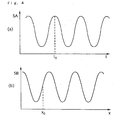
- the control system 9 may, by way of example, drive the wafer stage 6 in the directions X to scan the alignment mark 26 relative to the beam L2. This, as shown in Fig. 4(a) , makes the detected signal SA change sinusoidally as time t passes.
- the processing system 21A detects the phase of the detected signal SA at a predetermined point of time to to detect the position of the alignment mark 26.
- the image pickup signal SB is sinusoidal as shown in Fig. 4(b) , where the horizontal axis represents the positions x on the image pickup device 19 in the direction corresponding to the direction (X) of measurement of the alignment mark 26, not time t.
- the alignment signal processing system 21B detects the phase of the pickup signal SB at a predetermined reference point x 0 on the image pickup plane to detect the position of the alignment mark 26. This embodiment makes it possible to accurately detect the position of the alignment mark 26, with beams transmitted by the polysilicon film covering the mark.
- the reference grating 18 might be formed on the reticle 2 so that the wafer 4 and the reticle R could be directly aligned with each other by the TTR (through the reticle) system.
- Fig. 5 shows a method or process for forming alignment marks 26 to be detected in the foregoing embodiments.
- a wafer 4 which is a silicon substrate is coated with photoresist 22.
- the photoresist 22 is exposed through a reticle pattern image by an exposure apparatus.
- the photoresist 22 is developed to have spaces 22a - 22c of predetermined width formed in its portion corresponding to a circuit pattern area, and narrower spaces 22d formed at the pitch P ( Fig. 1(b) ) in its portion corresponding to the alignment marks.
- an insulating film 25 made of dielectric such as silicon dioxide (SiO 2 ) is formed on the wafer 4. Thereafter, the outer surface of the insulating film 25 is processed by the CMP process so that, as shown in Fig. 5(e) , the film is partially removed and flattened until the wafer surface 4a appears or is exposed. As a result, a circuit pattern 29 is formed in the form of insulators 25a - 25c embedded in the wider recesses in the circuit pattern area of the wafer 4, while an alignment mark 26 is formed in the form of insulators 25d embedded in the recesses formed at the pitch P in the alignment mark area of the wafer.
- dielectric silicon dioxide
- the first to third steps constitute the STI (shallow trench isolation) process.
- the insulators 25a - 25c in the circuit pattern area 29 serve to insulate adjacent minute elements from each other.
- a predetermined minute circuit pattern is formed between the insulators 25a - 25c, for example, at the step before or after this step.
- a polysilicon film 27 is formed on this surface as shown in Fig. 5(f) .
- the outer surface of this film is coated with photoresist 28 as shown in Fig. 5(g) .
- the alignment mark 26 at this stage is in the same condition as the mark 26 shown in Fig. 1(b) is.
- superposing exposure is performed, for example, by the projection exposure apparatus shown in Fig. 1 .
- this method of mark formation makes it possible to form alignment marks 26 efficiently while forming a circuit pattern by the STI (shallow trench isolation) process.
- the alignment mark 26 is formed together with the circuit pattern 29 directly in the surface of the wafer 4.
- the wafer 4 might be stacked with layers, one of which might have recesses formed in it. Insulators or the like might be embedded in the recesses to form an alignment mark, to which the invention could be applied with similar effect.
- Each of the exposure apparatus according to the embodiments may be replaced with an exposure apparatus employing the proximity system for exposure through the pattern on a mask with the mask and a substrate close or adjacent to each other without a projection optical system used.
- the present invention can also be applied to this case.
- the exposure apparatus are not limited to exposure apparatus for making semiconductors, but may be a variety of exposure apparatus such as liquid crystal exposure apparatus for exposing rectangular glass plates through liquid crystal display element patterns and exposure apparatus for making thin-film magnetic heads.
- the exposure apparatus may be exposure apparatus using X-rays or extreme ultraviolet (EUV) rays, such as soft X-rays, as exposure light, or electron beam exposure apparatus using electron beams as exposure beams.
- EUV extreme ultraviolet
- the projection optical system In the case of a projection optical system used, its magnifying power may be any of reduction, one (equal) magnification and enlargement. If far ultraviolet rays such as excimer laser beams are used, the projection optical system is composed of quartz, fluorite or other material which transmits far ultraviolet rays. If F 2 laser beams or X-rays are used, the projection optical system is catadioptric or catoptric (with a reflecting reticle used). If electron beams are used, the optical systems may be electro-optical systems each consisting of an electron lens and a deflector. Of course, the optical paths through which electron beams pass are vacuum.
- the exposure apparatus it is possible to produce the exposure apparatus according to each of the embodiments by incorporating an illuminating optical system, which consists of lenses, and a projection optical system into the apparatus body, making an optical adjustment, fitting the body with a reticle stage and a wafer stage, which consist of a large number of mechanical parts, connecting wires and pipes or tubes, and making a general adjustment (electric/al adjustment, operation confirmation, etc.). It is preferable that the exposure apparatus be produced in a clean room where the temperature and the cleanness are controlled.
- an illuminating optical system which consists of lenses
- a projection optical system into the apparatus body, making an optical adjustment, fitting the body with a reticle stage and a wafer stage, which consist of a large number of mechanical parts, connecting wires and pipes or tubes, and making a general adjustment (electric/al adjustment, operation confirmation, etc.).
- the exposure apparatus be produced in a clean room where the temperature and the cleanness are controlled.
- the processing includes the step of designing the function and performance of the device, the step of producing a reticle on the basis of the designing step, the step of making a wafer out of silicon, the step of exposing the wafer through the pattern on the reticle while the wafer and the reticle are aligned by the associated exposure apparatus, the step of assembling the device (which includes dicing, bonding and packaging it), and the step of inspecting the product.
- the alignment mark is irradiated with one coherent light beam, it is possible to detect the mark position accurately on a time base or a position base, respectively, by radiating the pair of diffracted light beams from the mark at a predetermined angle of intersection onto a predetermined diffraction grating, and detecting the photoelectrically converted signal of the diffracted light produced from this grating, or by radiating the pair of diffracted light beams from the mark at a predetermined angle of intersection onto a predetermined observation or monitoring plane or surface so as to form an image of interference fringes.
- the mark detection system according to the present invention can be used by the mark detection method according to the invention. Even for exposure of a substrate which transmits no visible light, the exposure apparatus according to the invention can perform accurate alignment by means of the mark detection system.
Landscapes
- Physics & Mathematics (AREA)
- General Physics & Mathematics (AREA)
- Exposure Of Semiconductors, Excluding Electron Or Ion Beam Exposure (AREA)
- Exposure And Positioning Against Photoresist Photosensitive Materials (AREA)
- Credit Cards Or The Like (AREA)
- Controlling Rewinding, Feeding, Winding, Or Abnormalities Of Webs (AREA)
- Testing Or Measuring Of Semiconductors Or The Like (AREA)
Claims (26)
- Verfahren zur Detektion einer Ausrichtmarke (26), die auf einem Substrat (4) gebildet ist, eine Ausnehmung (23d) aufweist und mit einem Film (27) bedeckt ist, mit den folgenden Schritten:Bestrahlen der Ausrichtmarke (26) mit einem kohärenten Lichtstrahl (L2; LA, LB), der eine Wellenlänge von 800 bis 1500 mm hat, durch den Film (27) hindurch,Empfangen von gebeugtem Licht (LDA, LDB; LD), das durch die Bestrahlung der Ausrichtmarke mit dem kohärenten Strahl erzeugt wurde, undDetektieren von Positionsinformation über die Ausrichtmarke auf der Grundlage des empfangenen gebeugten Lichts,dadurch gekennzeichnet, daß
der Film (26) kein sichtbares Licht durchläßt und
ein Isolator (25d) in die Ausnehmung (23d) eingebettet ist. - Verfahren nach Anspruch 1, bei dem die Ausrichtmarke (26) im STI (shallow trench isolation) Verfahren hergestellt ist.
- Verfahren nach Anspruch 1, bei dem der Film (27) aus Poly-Silizium hergestellt ist.
- Verfahren nach Anspruch 1, bei dem die Ausrichtmarke (26) mit zwei miteinander kohärenten Lichtstrahlen (LA, LB) bestrahlt wird und zwei gebeugte Lichtstrahlen (LD) empfangen werden, die durch die Bestrahlung mit den kohärenten Strahlen erzeugt werden und in derselben Richtung von der Ausrichtmarke ausgehen.
- Verfahren nach Anspruch 1, bei dem die Ausrichtmarke mit einem kohärenten Lichtstrahl (L2) bestrahlt wird und zwei gebeugte Lichtstrahlen (LDA, LDD) empfangen werden, die von der Ausrichtmarke erzeugt werden und unterschiedliche Richtungen haben.
- Verfahren nach Anspruch 5, bei dem ein vorbestimmtes Beugungsgitter (18) unter einem vorbestimmten Schnittwinkel mit den beiden an der Ausrichtmarke (26) gebeugten Lichtstrahlen (LDA, LDD) bestrahlt wird und die Position der Ausrichtmarke anhand eines fotoelektrisch konvertierten Signals des an dem Beugungsgitter gebeugten Lichts (LDC) detektiert wird.
- Verfahren nach Anspruch 4, bei dem die beiden miteinander kohärenten Lichtstrahlen (LA, LB) heterodyne Strahlen sind, die sich in ihrer Frequenz unterscheiden.
- Verfahren nach Anspruch 1, bei dem der kohärente Strahl einen ersten Lichtstrahl (LA) mit einer ersten Wellenlänge zwischen 800 und 1500 nm undeinen zweiten Lichtstrahl (LD) mit einer zweiten, von der ersten Wellenlänge verschiedenen Wellenlänge enthält und das durch die Bestrahlung der Ausrichtmarke mit dem zweiten Strahl erzeugte gebeugte Licht empfangen wird.
- Verfahren nach Anspruch 8, bei dem die zweite Wellenlänge eine Wellenlänge zwischen 500 und 1500 nm einschließt.
- Verfahren nach Anspruch 8, bei dem die zweite Wellenlänge eine Wellenlänge zwischen 500 und 800 nm einschließt.
- Verfahren nach Anspruch 8, bei dem die ersten und zweiten Strahlen mehrere Lichtstrahlen umfassen, die im wesentlichen die gleiche Wellenlänge haben und miteinander kohärent sind.
- Verfahren nach Anspruch 8, bei dem die Position der Ausrichtmarke detektiert wird auf der Grundlage des gebeugten Lichts, das durch die Bestrahlung der Ausrichtmarke mit dem ersten Strahl erzeugt wird, und/oder des gebeugten Lichts, das durch die Bestrahlung der Ausrichtmarke mit dem zweiten Strahl erzeugt wird.
- Verfahren zur Belichtung eines Substrats (4) mit einem vorbestimmten Muster (29), mit Ausrichtung des Substrats mit dem vorbestimmten Muster auf der Grundlage von Positionsinformation über die Ausrichtmarke, die nach dem Verfahren gemäß einem der Ansprüche 1 bis 12 detektiert wurde.
- Verfahren nach Anspruch 13, bei dem das vorbestimmte Muster durch ein Projektionssystem (PL) auf das Substrat (4) projiziert wird und das von der Ausrichtmarke erzeugte gebeugte Licht durch das Projektionssystem hindurch empfangen wird
- Verfahren nach Anspruch 14, bei dem das vorbestimmte Muster auf einer Maske (R) gebildet wird und das von der Ausrichtmarke erzeugte gebeugte Licht durch das Projektionssystem und die Maske hindurch empfangen wird.
- Verfahren nach Anspruch 13, bei dem das vorbestimmte Muster durch ein Projektionssystem (PL) auf das Substrat projiziert wird und das von der Ausrichtmarke erzeugte gebeugte Licht empfangen wird, ohne daß es durch das Projektionssystem hindurchgeht.
- Verfahren zur Herstellung eines Halbleiterbauelements mit Hilfe eines Prozesses zur Übertragung eines vorbestimmten Musters (29) durch Überlagern des vorbestimmten Musters durch ein Projektionssystem (PL) mit einem auf einem Substrat (4) gebildeten Muster, mit Verwendung des Belichtungsverfahrens nach Anspruch 13.
- System zur Detektion einer Markierung, mit:einem Markierungsdetektor,einer Ausrichtmarke (26), die auf einem Substrat gebildet ist, eine Ausnehmung (23d) aufweist und mit einem Film (27) bedeckt ist,einem Bestrahlungssystem (10-15, PL), das dazu ausgebildet ist, die Ausrichtmarke durch den Film (27) hindurch mit einem kohärenten Lichtstrahl (L2; LA, LB) zu bestrahlen, der eine Wellenlänge zwischen 800 und 1500 nm hat, undeinem Empfangssystem (PL, 15, 18), das dazu ausgebildet ist, gebeugtes Licht, das durch die Bestrahlung der Ausrichtmarke mit dem kohärenten Strahl erzeugt wurde, zu empfangen und Positionsinformation über die Ausrichtmarke auf der Grundlage des empfangenen gebeugten Lichts zu detektieren,dadurch gekennzeichnet, daß
der Film (27) kein sichtbares Licht durchläßt und
ein Isolator (25d) in die Ausnehmung (23d) eingebettet ist. - Detektionssystem nach Anspruch 18, bei dem die Ausrichtmarke (26) im STI-Verfahren hergestellt ist.
- Detektionssystem nach Anspruch 18, bei dem der Film (27) Poly-Silizium enthält.
- Detektionssystem nach Anspruch 18, bei dem das Bestrahlungssystem dazu ausgebildet ist, die Ausrichtmarke (26) mit zwei miteinander kohärenten Lichtstrahlen (LA, LD) zu bestrahlen, und das Empfangssystem dazu ausgebildet ist, zwei gebeugte Lichtstrahlen (LD) zu empfangen, die durch die Bestrahlung der Ausrichtmarke mit den kohärenten Strahlen erzeugt und in derselben Richtung emittiert werden.
- Detektionssystem nach Anspruch 18, bei dem das Bestrahlungssystem dazu ausgebildet ist, die Ausrichtmarke mit einem kohärenten Lichtstrahl (L2) zu bestrahlen, und das Empfangssystem dazu ausgebildet ist, zwei gebeugte Lichtstrahlen (LDA, LDD) zu empfangen, die von der Ausrichtmarke erzeugt werden und unterschiedliche Richtungen haben.
- Belichtungsgerät zur Belichtung eines Substrats (4) mit einem vorbestimmten Muster, das ein Markierungsdetektionssystem nach einem der Ansprüche 18-22 aufweist und dazu ausgebildet ist, das Substrat auf der Grundlage von Positionsinformation über die Ausrichtmarke, die mit Hilfe des Markierungsdetektors gewonnen wurde, mit dem vorbestimmten Muster auszurichten.
- Belichtungsgerät nach Anspruch 23, mit einem Projektionssystem (PL), das dazu ausgebildet ist, das vorbestimmte Muster auf das Substrat zu projizieren, wobei das Empfangssystem dazu ausgebildet ist, das gebeugte Licht, das von der Ausrichtmarke erzeugt wird, durch das Projektionssystem hindurch zu empfangen.
- Belichtungsgerät nach Anspruch 24, bei dem das vorbestimmte Muster (29) auf einer Maske (R) gebildet ist und das Empfangssystem dazu ausgebildet ist, das von der Ausrichtmarke erzeugte gebeugte Licht durch das Projektionssystem und die Maske hindurch zu empfangen.
- Belichtungsgerät nach Anspruch 23, mit einem Projektionssystem (PL), das dazu ausgebildet ist, das vorbestimmte Muster auf das Substrat zu projizieren, wobei das Empfangssystem dazu ausgebildet ist, das von der Ausrichtmarke erzeugte gebeugte Licht zu empfangen, ohne daß es durch das Projektionssystem hindurchgeht.
Applications Claiming Priority (3)
| Application Number | Priority Date | Filing Date | Title |
|---|---|---|---|
| JP31923997 | 1997-11-20 | ||
| JP31923997 | 1997-11-20 | ||
| PCT/JP1998/005226 WO1999027567A1 (en) | 1997-11-20 | 1998-11-19 | Mark detection method and mark position sensor |
Publications (3)
| Publication Number | Publication Date |
|---|---|
| EP1041608A1 EP1041608A1 (de) | 2000-10-04 |
| EP1041608A4 EP1041608A4 (de) | 2003-11-19 |
| EP1041608B1 true EP1041608B1 (de) | 2008-09-17 |
Family
ID=18107976
Family Applications (1)
| Application Number | Title | Priority Date | Filing Date |
|---|---|---|---|
| EP98954761A Expired - Lifetime EP1041608B1 (de) | 1997-11-20 | 1998-11-19 | Methode und System zur Detektion einer Marke |
Country Status (7)
| Country | Link |
|---|---|
| US (1) | US6285455B1 (de) |
| EP (1) | EP1041608B1 (de) |
| JP (1) | JP4192423B2 (de) |
| AT (1) | ATE408857T1 (de) |
| AU (1) | AU1174599A (de) |
| DE (1) | DE69840031D1 (de) |
| WO (1) | WO1999027567A1 (de) |
Families Citing this family (32)
| Publication number | Priority date | Publication date | Assignee | Title |
|---|---|---|---|---|
| EP1041608B1 (de) | 1997-11-20 | 2008-09-17 | Nikon Corporation | Methode und System zur Detektion einer Marke |
| US7057299B2 (en) * | 2000-02-03 | 2006-06-06 | Taiwan Semiconductor Manufacturing Co., Ltd. | Alignment mark configuration |
| KR100643225B1 (ko) * | 2000-04-28 | 2006-11-10 | 에이에스엠엘 네델란즈 비.브이. | 리소그래피 투영장치, 기판정렬 마크의 위치를 결정하는방법, 디바이스 제조방법 및 그 디바이스 |
| KR100500469B1 (ko) * | 2001-01-12 | 2005-07-12 | 삼성전자주식회사 | 정렬마크와 이를 이용하는 노광정렬시스템 및 그 정렬방법 |
| US6633048B2 (en) * | 2001-05-03 | 2003-10-14 | Northrop Grumman Corporation | High output extreme ultraviolet source |
| US20040005769A1 (en) * | 2002-07-03 | 2004-01-08 | Cabot Microelectronics Corp. | Method and apparatus for endpoint detection |
| KR100632889B1 (ko) * | 2002-09-20 | 2006-10-13 | 에이에스엠엘 네델란즈 비.브이. | 2개이상의 파장을 사용하는 리소그래피시스템용정렬시스템 및 정렬방법 |
| US6774452B1 (en) | 2002-12-17 | 2004-08-10 | Cypress Semiconductor Corporation | Semiconductor structure having alignment marks with shallow trench isolation |
| KR100519948B1 (ko) * | 2003-05-20 | 2005-10-10 | 엘지.필립스 엘시디 주식회사 | 비정질 실리콘의 결정화 공정 및 이를 이용한 스위칭 소자 |
| DE10356519A1 (de) * | 2003-12-03 | 2005-07-07 | Infineon Technologies Ag | Verfahren und optisches System zum Erfassen einer geometrischen Form auf einem Halbleitersubstrat |
| US7565219B2 (en) * | 2003-12-09 | 2009-07-21 | Asml Netherlands B.V. | Lithographic apparatus, method of determining a model parameter, device manufacturing method, and device manufactured thereby |
| JP4777731B2 (ja) * | 2005-03-31 | 2011-09-21 | 富士通セミコンダクター株式会社 | 半導体装置の製造方法 |
| US7612892B2 (en) * | 2005-10-06 | 2009-11-03 | Nikon Corporation | Imaging optical system configured with through the lens optics for producing control information |
| JP5425363B2 (ja) * | 2006-11-28 | 2014-02-26 | ルネサスエレクトロニクス株式会社 | 半導体装置、及び表示装置 |
| JP4966719B2 (ja) | 2007-04-11 | 2012-07-04 | 株式会社日立ハイテクノロジーズ | 校正用標準部材及びその作製方法、並びにそれを用いた電子ビーム装置 |
| JP2008270072A (ja) * | 2007-04-24 | 2008-11-06 | Sii Nanotechnology Inc | 荷電粒子ビーム装置 |
| JP2009094512A (ja) * | 2007-10-09 | 2009-04-30 | Asml Netherlands Bv | 位置合わせ方法及び装置、リソグラフィ装置、計測装置、及びデバイス製造方法 |
| CN101435997B (zh) * | 2007-11-15 | 2012-06-27 | 上海华虹Nec电子有限公司 | 光刻套刻精度的测试图形及测量方法 |
| NL1036179A1 (nl) * | 2007-11-20 | 2009-05-25 | Asml Netherlands Bv | Lithographic apparatus and method. |
| JP5406624B2 (ja) * | 2009-08-10 | 2014-02-05 | キヤノン株式会社 | 検出装置、露光装置及びデバイスの製造方法 |
| US8088633B2 (en) * | 2009-12-02 | 2012-01-03 | Ultratech, Inc. | Optical alignment methods for forming LEDs having a rough surface |
| CN102243442B (zh) * | 2010-05-12 | 2014-11-12 | 上海微电子装备有限公司 | 硅片对准光源幅度调制装置 |
| US8422027B2 (en) | 2010-06-08 | 2013-04-16 | Nikon Corporation | Imaging optical system for producing control information regarding lateral movement of an image plane or an object plane |
| DE102013220190B4 (de) * | 2013-10-07 | 2021-08-12 | Dr. Johannes Heidenhain Gmbh | Messteilung und lichtelektrische Positionsmesseinrichtung mit dieser Messteilung |
| CN104359410B (zh) * | 2014-12-01 | 2017-05-17 | 清华大学 | 一种利用可旋转光栅测量的位移测量系统 |
| JP6378117B2 (ja) * | 2015-03-13 | 2018-08-22 | 東芝メモリ株式会社 | アライメントマークの形成方法および半導体装置 |
| WO2017125352A1 (en) | 2016-01-19 | 2017-07-27 | Asml Netherlands B.V. | Position sensing arrangement and lithographic apparatus including such an arrangement, position sensing method and device manufacturing method |
| NL2019155A (en) * | 2016-08-30 | 2018-03-06 | Asml Netherlands Bv | Position sensor, lithographic apparatus and method for manufacturing devices |
| JP6791584B2 (ja) * | 2017-02-01 | 2020-11-25 | 株式会社ディスコ | 加工方法 |
| JP6584567B1 (ja) * | 2018-03-30 | 2019-10-02 | キヤノン株式会社 | リソグラフィ装置、パターン形成方法及び物品の製造方法 |
| US12372879B2 (en) * | 2021-12-17 | 2025-07-29 | Micron Technology, Inc. | Apparatuses and methods for diffraction base overlay measurements |
| US20230296994A1 (en) * | 2022-03-21 | 2023-09-21 | Infineon Technologies Ag | Back Side to Front Side Alignment on a Semiconductor Wafer with Special Structures |
Citations (1)
| Publication number | Priority date | Publication date | Assignee | Title |
|---|---|---|---|---|
| US5861320A (en) * | 1995-03-10 | 1999-01-19 | Nikon Corporation | Position detection mark and position detection method |
Family Cites Families (10)
| Publication number | Priority date | Publication date | Assignee | Title |
|---|---|---|---|---|
| JPS63240018A (ja) | 1987-03-27 | 1988-10-05 | Matsushita Electric Ind Co Ltd | アライメント方法 |
| JP2773147B2 (ja) * | 1988-08-19 | 1998-07-09 | 株式会社ニコン | 露光装置の位置合わせ装置及び方法 |
| JP2906433B2 (ja) | 1989-04-25 | 1999-06-21 | 株式会社ニコン | 投影露光装置及び投影露光方法 |
| US5151750A (en) | 1989-04-14 | 1992-09-29 | Nikon Corporation | Alignment apparatus |
| JPH032504A (ja) * | 1989-05-30 | 1991-01-08 | Nikon Corp | 位置合わせ装置 |
| JPH05326360A (ja) * | 1992-05-20 | 1993-12-10 | Victor Co Of Japan Ltd | 半導体装置の製造方法及び製造装置 |
| JPH06260389A (ja) | 1993-03-05 | 1994-09-16 | Nikon Corp | アライメント装置 |
| JPH07321030A (ja) | 1994-03-29 | 1995-12-08 | Nikon Corp | アライメント装置 |
| US5721605A (en) | 1994-03-29 | 1998-02-24 | Nikon Corporation | Alignment device and method with focus detection system |
| EP1041608B1 (de) | 1997-11-20 | 2008-09-17 | Nikon Corporation | Methode und System zur Detektion einer Marke |
-
1998
- 1998-11-19 EP EP98954761A patent/EP1041608B1/de not_active Expired - Lifetime
- 1998-11-19 AT AT98954761T patent/ATE408857T1/de not_active IP Right Cessation
- 1998-11-19 DE DE69840031T patent/DE69840031D1/de not_active Expired - Lifetime
- 1998-11-19 AU AU11745/99A patent/AU1174599A/en not_active Abandoned
- 1998-11-19 WO PCT/JP1998/005226 patent/WO1999027567A1/ja not_active Ceased
- 1998-11-19 JP JP2000522614A patent/JP4192423B2/ja not_active Expired - Fee Related
-
2000
- 2000-05-19 US US09/573,223 patent/US6285455B1/en not_active Expired - Lifetime
Patent Citations (1)
| Publication number | Priority date | Publication date | Assignee | Title |
|---|---|---|---|---|
| US5861320A (en) * | 1995-03-10 | 1999-01-19 | Nikon Corporation | Position detection mark and position detection method |
Also Published As
| Publication number | Publication date |
|---|---|
| JP4192423B2 (ja) | 2008-12-10 |
| WO1999027567A1 (en) | 1999-06-03 |
| US6285455B1 (en) | 2001-09-04 |
| ATE408857T1 (de) | 2008-10-15 |
| EP1041608A1 (de) | 2000-10-04 |
| EP1041608A4 (de) | 2003-11-19 |
| DE69840031D1 (de) | 2008-10-30 |
| AU1174599A (en) | 1999-06-15 |
Similar Documents
| Publication | Publication Date | Title |
|---|---|---|
| US6285455B1 (en) | Mark detection method, optical system and mark position detector | |
| US20060250597A1 (en) | Positional information measuring method and device, and exposure method and apparatus | |
| US6421124B1 (en) | Position detecting system and device manufacturing method using the same | |
| JPWO1999027567A1 (ja) | マーク検出方法、及び位置検出装置 | |
| US7656503B2 (en) | Exposure apparatus and image plane detecting method | |
| KR100517159B1 (ko) | 노광장치 및 방법 | |
| JP3254916B2 (ja) | 投影光学系のコマ収差を検出する方法 | |
| JPH11150063A (ja) | 位置ずれ検出方法及びそれを用いたデバイスの製造方法 | |
| JP2010098143A (ja) | 露光装置およびデバイス製造方法 | |
| KR20010091971A (ko) | 얼라인먼트 장치, 얼라인먼트 방법, 노광 장치 및 노광 방법 | |
| JPH1070068A (ja) | 位置合わせ方法及びそれを用いた投影露光装置 | |
| WO2001065591A1 (en) | Position measuring apparatus and aligner | |
| US6714691B2 (en) | Exposure method and apparatus, and device manufacturing method using the same | |
| JPH09320921A (ja) | ベースライン量の測定方法及び投影露光装置 | |
| JP2003142377A (ja) | 投影露光装置及び収差の計測方法 | |
| JP3428705B2 (ja) | 位置検出装置及びそれを用いた半導体素子の製造方法 | |
| US20050231703A1 (en) | Exposure apparatus, and device manufacturing method | |
| JP2006339448A (ja) | 受光ユニットを有する露光装置 | |
| JPH0963924A (ja) | アライメント方法 | |
| JP4311713B2 (ja) | 露光装置 | |
| JPH1140493A (ja) | 走査型露光装置およびデバイス製造方法 | |
| TW202244461A (zh) | 測量設備、曝光設備及物品製造方法 | |
| JP2005175383A (ja) | 露光装置、アライメント方法、及び、デバイスの製造方法 | |
| JP3667009B2 (ja) | 露光装置及びそれを用いたデバイスの製造方法 | |
| JP3039305B2 (ja) | 位置合わせ装置及びそれを用いた半導体デバイスの製造方法 |
Legal Events
| Date | Code | Title | Description |
|---|---|---|---|
| PUAI | Public reference made under article 153(3) epc to a published international application that has entered the european phase |
Free format text: ORIGINAL CODE: 0009012 |
|
| 17P | Request for examination filed |
Effective date: 20000526 |
|
| AK | Designated contracting states |
Kind code of ref document: A1 Designated state(s): AT BE CH CY DE DK ES FI FR GB GR IE IT LI LU MC NL PT SE |
|
| A4 | Supplementary search report drawn up and despatched |
Effective date: 20031002 |
|
| 17Q | First examination report despatched |
Effective date: 20040205 |
|
| 17Q | First examination report despatched |
Effective date: 20040205 |
|
| RIC1 | Information provided on ipc code assigned before grant |
Ipc: G03F 9/00 20060101AFI20080225BHEP |
|
| RTI1 | Title (correction) |
Free format text: METHOD AND SYSTEM FOR DETECTING A MARK |
|
| GRAP | Despatch of communication of intention to grant a patent |
Free format text: ORIGINAL CODE: EPIDOSNIGR1 |
|
| GRAC | Information related to communication of intention to grant a patent modified |
Free format text: ORIGINAL CODE: EPIDOSCIGR1 |
|
| GRAS | Grant fee paid |
Free format text: ORIGINAL CODE: EPIDOSNIGR3 |
|
| GRAA | (expected) grant |
Free format text: ORIGINAL CODE: 0009210 |
|
| AK | Designated contracting states |
Kind code of ref document: B1 Designated state(s): AT BE CH CY DE DK ES FI FR GB GR IE IT LI LU MC NL PT SE |
|
| REG | Reference to a national code |
Ref country code: GB Ref legal event code: FG4D |
|
| REG | Reference to a national code |
Ref country code: CH Ref legal event code: EP |
|
| REG | Reference to a national code |
Ref country code: IE Ref legal event code: FG4D |
|
| REF | Corresponds to: |
Ref document number: 69840031 Country of ref document: DE Date of ref document: 20081030 Kind code of ref document: P |
|
| PG25 | Lapsed in a contracting state [announced via postgrant information from national office to epo] |
Ref country code: FI Free format text: LAPSE BECAUSE OF FAILURE TO SUBMIT A TRANSLATION OF THE DESCRIPTION OR TO PAY THE FEE WITHIN THE PRESCRIBED TIME-LIMIT Effective date: 20080917 Ref country code: AT Free format text: LAPSE BECAUSE OF FAILURE TO SUBMIT A TRANSLATION OF THE DESCRIPTION OR TO PAY THE FEE WITHIN THE PRESCRIBED TIME-LIMIT Effective date: 20080917 |
|
| PG25 | Lapsed in a contracting state [announced via postgrant information from national office to epo] |
Ref country code: BE Free format text: LAPSE BECAUSE OF FAILURE TO SUBMIT A TRANSLATION OF THE DESCRIPTION OR TO PAY THE FEE WITHIN THE PRESCRIBED TIME-LIMIT Effective date: 20080917 |
|
| PG25 | Lapsed in a contracting state [announced via postgrant information from national office to epo] |
Ref country code: ES Free format text: LAPSE BECAUSE OF FAILURE TO SUBMIT A TRANSLATION OF THE DESCRIPTION OR TO PAY THE FEE WITHIN THE PRESCRIBED TIME-LIMIT Effective date: 20081228 |
|
| PG25 | Lapsed in a contracting state [announced via postgrant information from national office to epo] |
Ref country code: PT Free format text: LAPSE BECAUSE OF FAILURE TO SUBMIT A TRANSLATION OF THE DESCRIPTION OR TO PAY THE FEE WITHIN THE PRESCRIBED TIME-LIMIT Effective date: 20090217 |
|
| PG25 | Lapsed in a contracting state [announced via postgrant information from national office to epo] |
Ref country code: MC Free format text: LAPSE BECAUSE OF NON-PAYMENT OF DUE FEES Effective date: 20081130 |
|
| REG | Reference to a national code |
Ref country code: CH Ref legal event code: PL |
|
| PLBE | No opposition filed within time limit |
Free format text: ORIGINAL CODE: 0009261 |
|
| STAA | Information on the status of an ep patent application or granted ep patent |
Free format text: STATUS: NO OPPOSITION FILED WITHIN TIME LIMIT |
|
| PG25 | Lapsed in a contracting state [announced via postgrant information from national office to epo] |
Ref country code: DK Free format text: LAPSE BECAUSE OF FAILURE TO SUBMIT A TRANSLATION OF THE DESCRIPTION OR TO PAY THE FEE WITHIN THE PRESCRIBED TIME-LIMIT Effective date: 20080917 |
|
| 26N | No opposition filed |
Effective date: 20090618 |
|
| PG25 | Lapsed in a contracting state [announced via postgrant information from national office to epo] |
Ref country code: IT Free format text: LAPSE BECAUSE OF FAILURE TO SUBMIT A TRANSLATION OF THE DESCRIPTION OR TO PAY THE FEE WITHIN THE PRESCRIBED TIME-LIMIT Effective date: 20080917 |
|
| REG | Reference to a national code |
Ref country code: FR Ref legal event code: ST Effective date: 20090731 |
|
| PG25 | Lapsed in a contracting state [announced via postgrant information from national office to epo] |
Ref country code: LI Free format text: LAPSE BECAUSE OF NON-PAYMENT OF DUE FEES Effective date: 20081130 Ref country code: IE Free format text: LAPSE BECAUSE OF NON-PAYMENT OF DUE FEES Effective date: 20081119 Ref country code: CH Free format text: LAPSE BECAUSE OF NON-PAYMENT OF DUE FEES Effective date: 20081130 |
|
| PG25 | Lapsed in a contracting state [announced via postgrant information from national office to epo] |
Ref country code: SE Free format text: LAPSE BECAUSE OF FAILURE TO SUBMIT A TRANSLATION OF THE DESCRIPTION OR TO PAY THE FEE WITHIN THE PRESCRIBED TIME-LIMIT Effective date: 20081217 |
|
| PG25 | Lapsed in a contracting state [announced via postgrant information from national office to epo] |
Ref country code: LU Free format text: LAPSE BECAUSE OF NON-PAYMENT OF DUE FEES Effective date: 20081119 |
|
| PG25 | Lapsed in a contracting state [announced via postgrant information from national office to epo] |
Ref country code: CY Free format text: LAPSE BECAUSE OF FAILURE TO SUBMIT A TRANSLATION OF THE DESCRIPTION OR TO PAY THE FEE WITHIN THE PRESCRIBED TIME-LIMIT Effective date: 20080917 |
|
| PG25 | Lapsed in a contracting state [announced via postgrant information from national office to epo] |
Ref country code: GR Free format text: LAPSE BECAUSE OF FAILURE TO SUBMIT A TRANSLATION OF THE DESCRIPTION OR TO PAY THE FEE WITHIN THE PRESCRIBED TIME-LIMIT Effective date: 20081218 |
|
| PG25 | Lapsed in a contracting state [announced via postgrant information from national office to epo] |
Ref country code: FR Free format text: LAPSE BECAUSE OF NON-PAYMENT OF DUE FEES Effective date: 20081130 |
|
| PGFP | Annual fee paid to national office [announced via postgrant information from national office to epo] |
Ref country code: DE Payment date: 20121114 Year of fee payment: 15 |
|
| PGFP | Annual fee paid to national office [announced via postgrant information from national office to epo] |
Ref country code: GB Payment date: 20121114 Year of fee payment: 15 |
|
| PGFP | Annual fee paid to national office [announced via postgrant information from national office to epo] |
Ref country code: NL Payment date: 20121116 Year of fee payment: 15 |
|
| REG | Reference to a national code |
Ref country code: NL Ref legal event code: V1 Effective date: 20140601 |
|
| GBPC | Gb: european patent ceased through non-payment of renewal fee |
Effective date: 20131119 |
|
| PG25 | Lapsed in a contracting state [announced via postgrant information from national office to epo] |
Ref country code: NL Free format text: LAPSE BECAUSE OF NON-PAYMENT OF DUE FEES Effective date: 20140601 Ref country code: DE Free format text: LAPSE BECAUSE OF NON-PAYMENT OF DUE FEES Effective date: 20140603 |
|
| REG | Reference to a national code |
Ref country code: DE Ref legal event code: R119 Ref document number: 69840031 Country of ref document: DE Effective date: 20140603 |
|
| PG25 | Lapsed in a contracting state [announced via postgrant information from national office to epo] |
Ref country code: GB Free format text: LAPSE BECAUSE OF NON-PAYMENT OF DUE FEES Effective date: 20131119 |