EP0984316A2 - Halbleitervorrichtung und ihr Herstellungsverfahren - Google Patents
Halbleitervorrichtung und ihr Herstellungsverfahren Download PDFInfo
- Publication number
- EP0984316A2 EP0984316A2 EP99306912A EP99306912A EP0984316A2 EP 0984316 A2 EP0984316 A2 EP 0984316A2 EP 99306912 A EP99306912 A EP 99306912A EP 99306912 A EP99306912 A EP 99306912A EP 0984316 A2 EP0984316 A2 EP 0984316A2
- Authority
- EP
- European Patent Office
- Prior art keywords
- bias
- lines
- line
- photoelectric conversion
- pixel
- Prior art date
- Legal status (The legal status is an assumption and is not a legal conclusion. Google has not performed a legal analysis and makes no representation as to the accuracy of the status listed.)
- Withdrawn
Links
- 238000004519 manufacturing process Methods 0.000 title claims abstract description 25
- 239000004065 semiconductor Substances 0.000 title claims description 50
- 239000011159 matrix material Substances 0.000 claims abstract description 43
- 239000003990 capacitor Substances 0.000 claims abstract description 28
- 229910052751 metal Inorganic materials 0.000 claims abstract description 20
- 239000002184 metal Substances 0.000 claims abstract description 20
- 238000006243 chemical reaction Methods 0.000 claims description 88
- 230000007547 defect Effects 0.000 claims description 25
- 239000010409 thin film Substances 0.000 claims description 20
- 239000000758 substrate Substances 0.000 claims description 17
- 238000000034 method Methods 0.000 claims description 16
- 238000012546 transfer Methods 0.000 claims description 13
- 230000002950 deficient Effects 0.000 claims description 10
- 239000004020 conductor Substances 0.000 claims 3
- 238000010586 diagram Methods 0.000 description 30
- 239000010410 layer Substances 0.000 description 20
- 230000003247 decreasing effect Effects 0.000 description 8
- 239000011651 chromium Substances 0.000 description 7
- 230000005484 gravity Effects 0.000 description 7
- 238000012545 processing Methods 0.000 description 7
- 239000010408 film Substances 0.000 description 5
- 239000004973 liquid crystal related substance Substances 0.000 description 5
- 238000005520 cutting process Methods 0.000 description 4
- 230000000694 effects Effects 0.000 description 4
- 239000011295 pitch Substances 0.000 description 4
- 238000001514 detection method Methods 0.000 description 3
- 238000007689 inspection Methods 0.000 description 3
- 239000000463 material Substances 0.000 description 3
- 230000015572 biosynthetic process Effects 0.000 description 2
- 230000001066 destructive effect Effects 0.000 description 2
- 238000003745 diagnosis Methods 0.000 description 2
- 239000011241 protective layer Substances 0.000 description 2
- 230000035945 sensitivity Effects 0.000 description 2
- 238000003860 storage Methods 0.000 description 2
- MINPZZUPSSVGJN-UHFFFAOYSA-N 1,1,1,4,4,4-hexachlorobutane Chemical compound ClC(Cl)(Cl)CCC(Cl)(Cl)Cl MINPZZUPSSVGJN-UHFFFAOYSA-N 0.000 description 1
- AGCPZMJBXSCWQY-UHFFFAOYSA-N 1,1,2,3,4-pentachlorobutane Chemical compound ClCC(Cl)C(Cl)C(Cl)Cl AGCPZMJBXSCWQY-UHFFFAOYSA-N 0.000 description 1
- 229920000049 Carbon (fiber) Polymers 0.000 description 1
- VYZAMTAEIAYCRO-UHFFFAOYSA-N Chromium Chemical compound [Cr] VYZAMTAEIAYCRO-UHFFFAOYSA-N 0.000 description 1
- 101150049492 DVR gene Proteins 0.000 description 1
- 229910052782 aluminium Inorganic materials 0.000 description 1
- XAGFODPZIPBFFR-UHFFFAOYSA-N aluminium Chemical compound [Al] XAGFODPZIPBFFR-UHFFFAOYSA-N 0.000 description 1
- 238000003491 array Methods 0.000 description 1
- 230000005540 biological transmission Effects 0.000 description 1
- 239000004917 carbon fiber Substances 0.000 description 1
- 230000015556 catabolic process Effects 0.000 description 1
- 229910052804 chromium Inorganic materials 0.000 description 1
- 238000006731 degradation reaction Methods 0.000 description 1
- 238000013461 design Methods 0.000 description 1
- 238000011161 development Methods 0.000 description 1
- 230000005611 electricity Effects 0.000 description 1
- 238000005516 engineering process Methods 0.000 description 1
- 238000003702 image correction Methods 0.000 description 1
- 239000012212 insulator Substances 0.000 description 1
- 230000015654 memory Effects 0.000 description 1
- VNWKTOKETHGBQD-UHFFFAOYSA-N methane Chemical compound C VNWKTOKETHGBQD-UHFFFAOYSA-N 0.000 description 1
- 238000012986 modification Methods 0.000 description 1
- 230000004048 modification Effects 0.000 description 1
- 230000003287 optical effect Effects 0.000 description 1
- 230000000737 periodic effect Effects 0.000 description 1
- 230000004044 response Effects 0.000 description 1
- 230000003068 static effect Effects 0.000 description 1
Images


Classifications
-
- H—ELECTRICITY
- H04—ELECTRIC COMMUNICATION TECHNIQUE
- H04N—PICTORIAL COMMUNICATION, e.g. TELEVISION
- H04N5/00—Details of television systems
- H04N5/30—Transforming light or analogous information into electric information
- H04N5/32—Transforming X-rays
-
- G—PHYSICS
- G02—OPTICS
- G02F—OPTICAL DEVICES OR ARRANGEMENTS FOR THE CONTROL OF LIGHT BY MODIFICATION OF THE OPTICAL PROPERTIES OF THE MEDIA OF THE ELEMENTS INVOLVED THEREIN; NON-LINEAR OPTICS; FREQUENCY-CHANGING OF LIGHT; OPTICAL LOGIC ELEMENTS; OPTICAL ANALOGUE/DIGITAL CONVERTERS
- G02F1/00—Devices or arrangements for the control of the intensity, colour, phase, polarisation or direction of light arriving from an independent light source, e.g. switching, gating or modulating; Non-linear optics
- G02F1/01—Devices or arrangements for the control of the intensity, colour, phase, polarisation or direction of light arriving from an independent light source, e.g. switching, gating or modulating; Non-linear optics for the control of the intensity, phase, polarisation or colour
- G02F1/13—Devices or arrangements for the control of the intensity, colour, phase, polarisation or direction of light arriving from an independent light source, e.g. switching, gating or modulating; Non-linear optics for the control of the intensity, phase, polarisation or colour based on liquid crystals, e.g. single liquid crystal display cells
- G02F1/133—Constructional arrangements; Operation of liquid crystal cells; Circuit arrangements
- G02F1/136—Liquid crystal cells structurally associated with a semi-conducting layer or substrate, e.g. cells forming part of an integrated circuit
- G02F1/1362—Active matrix addressed cells
- G02F1/136204—Arrangements to prevent high voltage or static electricity failures
-
- H—ELECTRICITY
- H04—ELECTRIC COMMUNICATION TECHNIQUE
- H04N—PICTORIAL COMMUNICATION, e.g. TELEVISION
- H04N23/00—Cameras or camera modules comprising electronic image sensors; Control thereof
- H04N23/30—Cameras or camera modules comprising electronic image sensors; Control thereof for generating image signals from X-rays
-
- G—PHYSICS
- G02—OPTICS
- G02F—OPTICAL DEVICES OR ARRANGEMENTS FOR THE CONTROL OF LIGHT BY MODIFICATION OF THE OPTICAL PROPERTIES OF THE MEDIA OF THE ELEMENTS INVOLVED THEREIN; NON-LINEAR OPTICS; FREQUENCY-CHANGING OF LIGHT; OPTICAL LOGIC ELEMENTS; OPTICAL ANALOGUE/DIGITAL CONVERTERS
- G02F1/00—Devices or arrangements for the control of the intensity, colour, phase, polarisation or direction of light arriving from an independent light source, e.g. switching, gating or modulating; Non-linear optics
- G02F1/01—Devices or arrangements for the control of the intensity, colour, phase, polarisation or direction of light arriving from an independent light source, e.g. switching, gating or modulating; Non-linear optics for the control of the intensity, phase, polarisation or colour
- G02F1/13—Devices or arrangements for the control of the intensity, colour, phase, polarisation or direction of light arriving from an independent light source, e.g. switching, gating or modulating; Non-linear optics for the control of the intensity, phase, polarisation or colour based on liquid crystals, e.g. single liquid crystal display cells
- G02F1/133—Constructional arrangements; Operation of liquid crystal cells; Circuit arrangements
- G02F1/136—Liquid crystal cells structurally associated with a semi-conducting layer or substrate, e.g. cells forming part of an integrated circuit
- G02F1/1362—Active matrix addressed cells
- G02F1/136259—Repairing; Defects
-
- G—PHYSICS
- G09—EDUCATION; CRYPTOGRAPHY; DISPLAY; ADVERTISING; SEALS
- G09G—ARRANGEMENTS OR CIRCUITS FOR CONTROL OF INDICATING DEVICES USING STATIC MEANS TO PRESENT VARIABLE INFORMATION
- G09G2330/00—Aspects of power supply; Aspects of display protection and defect management
- G09G2330/08—Fault-tolerant or redundant circuits, or circuits in which repair of defects is prepared
-
- G—PHYSICS
- G09—EDUCATION; CRYPTOGRAPHY; DISPLAY; ADVERTISING; SEALS
- G09G—ARRANGEMENTS OR CIRCUITS FOR CONTROL OF INDICATING DEVICES USING STATIC MEANS TO PRESENT VARIABLE INFORMATION
- G09G3/00—Control arrangements or circuits, of interest only in connection with visual indicators other than cathode-ray tubes
- G09G3/20—Control arrangements or circuits, of interest only in connection with visual indicators other than cathode-ray tubes for presentation of an assembly of a number of characters, e.g. a page, by composing the assembly by combination of individual elements arranged in a matrix no fixed position being assigned to or needed to be assigned to the individual characters or partial characters
- G09G3/34—Control arrangements or circuits, of interest only in connection with visual indicators other than cathode-ray tubes for presentation of an assembly of a number of characters, e.g. a page, by composing the assembly by combination of individual elements arranged in a matrix no fixed position being assigned to or needed to be assigned to the individual characters or partial characters by control of light from an independent source
- G09G3/36—Control arrangements or circuits, of interest only in connection with visual indicators other than cathode-ray tubes for presentation of an assembly of a number of characters, e.g. a page, by composing the assembly by combination of individual elements arranged in a matrix no fixed position being assigned to or needed to be assigned to the individual characters or partial characters by control of light from an independent source using liquid crystals
- G09G3/3611—Control of matrices with row and column drivers
- G09G3/3648—Control of matrices with row and column drivers using an active matrix
Definitions
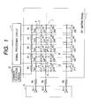
- Fig. 1 shows an example of equivalent circuitry of a TFT matrix panel.
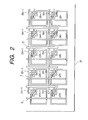
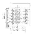
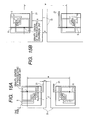
- Fig. 4 is a schematic pattern diagram at a corner part on the opposite side to the bias application side to the bias lines 6 by the common electrode driver 12 in the TFT panel of Fig. 3.
- the TFT matrix panel is constructed in the matrix of m ⁇ n, and potential configurations are m ⁇ 2, n ⁇ 1 in Embodiment 1 and m ⁇ 4, n ⁇ 1 in Embodiment 2.
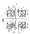
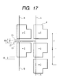
- Fig. 14 is a schematic pattern diagram at panel corners where the four TFT panels of Fig. 11 are placed with their corners meeting together.
Applications Claiming Priority (4)
| Application Number | Priority Date | Filing Date | Title |
|---|---|---|---|
| JP24721798 | 1998-09-01 | ||
| JP24721798 | 1998-09-01 | ||
| JP23576899 | 1999-08-23 | ||
| JP23576899A JP4401488B2 (ja) | 1998-09-01 | 1999-08-23 | 光電変換装置 |
Publications (2)
| Publication Number | Publication Date |
|---|---|
| EP0984316A2 true EP0984316A2 (de) | 2000-03-08 |
| EP0984316A3 EP0984316A3 (de) | 2004-06-02 |
Family
ID=26532318
Family Applications (1)
| Application Number | Title | Priority Date | Filing Date |
|---|---|---|---|
| EP99306912A Withdrawn EP0984316A3 (de) | 1998-09-01 | 1999-08-31 | Halbleitervorrichtung und ihr Herstellungsverfahren |
Country Status (3)
| Country | Link |
|---|---|
| US (2) | US6295142B1 (de) |
| EP (1) | EP0984316A3 (de) |
| JP (1) | JP4401488B2 (de) |
Cited By (2)
| Publication number | Priority date | Publication date | Assignee | Title |
|---|---|---|---|---|
| EP1850582A1 (de) | 2006-04-27 | 2007-10-31 | Canon Kabushiki Kaisha | Bildgebungsvorrichtung, Strahlungsabbildungsvorrichtung und Strahlungsabbildungssystem |
| EP4283679A1 (de) * | 2022-03-30 | 2023-11-29 | Canon Kabushiki Kaisha | Strahlungsbildgebungsvorrichtung und strahlungsbildgebungssystem |
Families Citing this family (25)
| Publication number | Priority date | Publication date | Assignee | Title |
|---|---|---|---|---|
| JP2002050754A (ja) * | 2000-05-08 | 2002-02-15 | Canon Inc | 半導体装置とその製造方法、放射線検出装置とそれを用いた放射線検出システム |
| JP4681774B2 (ja) * | 2001-08-30 | 2011-05-11 | キヤノン株式会社 | 撮像素子、その撮像素子を用いた撮像装置、及びその撮像装置を用いた撮像システム |
| US7116319B2 (en) * | 2002-05-21 | 2006-10-03 | Canon Kabushiki Kaisha | Image forming apparatus and radiation detection system |
| US6746474B2 (en) * | 2002-05-31 | 2004-06-08 | Vahid Saadat | Apparatus and methods for cooling a region within the body |
| US20040246355A1 (en) * | 2003-06-06 | 2004-12-09 | Ji Ung Lee | Storage capacitor array for a solid state radiation imager |
| JP4067055B2 (ja) * | 2003-10-02 | 2008-03-26 | キヤノン株式会社 | 撮像装置及びその製造方法、放射線撮像装置、放射線撮像システム |
| KR100982121B1 (ko) * | 2003-12-23 | 2010-09-14 | 엘지디스플레이 주식회사 | 액정표시장치 및 그 구동방법 |
| JP4207858B2 (ja) | 2004-07-05 | 2009-01-14 | セイコーエプソン株式会社 | 半導体装置、表示装置及び電子機器 |
| US7282719B2 (en) * | 2004-09-30 | 2007-10-16 | Canon Kabushiki Kaisha | Image pickup apparatus and radiation image pickup apparatus |
| US7557355B2 (en) * | 2004-09-30 | 2009-07-07 | Canon Kabushiki Kaisha | Image pickup apparatus and radiation image pickup apparatus |
| JP2006209089A (ja) * | 2004-12-27 | 2006-08-10 | Toshiba Matsushita Display Technology Co Ltd | 表示装置 |
| DE102005007485B4 (de) * | 2005-02-17 | 2008-05-08 | Siemens Ag | Zwischenstecker für einen Detektor und Verfahren zur Durchführung einer Fehlersuche bei einem Detektor mit einem solchen Zwischenstecker |
| JP4773768B2 (ja) | 2005-08-16 | 2011-09-14 | キヤノン株式会社 | 放射線撮像装置、その制御方法及び放射線撮像システム |
| JP4498283B2 (ja) * | 2006-01-30 | 2010-07-07 | キヤノン株式会社 | 撮像装置、放射線撮像装置及びこれらの製造方法 |
| US7551215B2 (en) * | 2006-03-15 | 2009-06-23 | Dalsa Corporation | CMOS-based sensor apparatus with cells that comprise a redundancy facility that is selectively activatable for isolating a metal-to-metal short on the basis of externally applied control actuation |
| TWI420480B (zh) * | 2009-05-19 | 2013-12-21 | Au Optronics Corp | 光電裝置及其顯示器 |
| JP5400507B2 (ja) * | 2009-07-13 | 2014-01-29 | キヤノン株式会社 | 撮像装置及び放射線撮像システム |
| US20110164076A1 (en) * | 2010-01-06 | 2011-07-07 | Sang Tae Lee | Cost-effective display methods and apparatuses |
| JP2011238897A (ja) | 2010-04-13 | 2011-11-24 | Canon Inc | 検出装置及びその製造方法並びに検出システム |
| KR101736321B1 (ko) | 2010-12-22 | 2017-05-17 | 삼성디스플레이 주식회사 | 엑스레이 검출기용 박막 트랜지스터 어레이 기판 및 엑스레이 검출기 |
| JP2012182759A (ja) * | 2011-03-03 | 2012-09-20 | Konica Minolta Medical & Graphic Inc | 放射線検出パネルおよび放射線画像撮影装置 |
| JP5869113B2 (ja) * | 2012-05-30 | 2016-02-24 | 富士フイルム株式会社 | 放射線画像撮影装置および放射線検出器 |
| US11710748B2 (en) | 2015-01-27 | 2023-07-25 | Beijing Boe Optoelectronics Technology Co., Ltd. | Array substrate and touch panel and manufacturing method of array substrate |
| CN104536636B (zh) * | 2015-01-27 | 2017-12-08 | 京东方科技集团股份有限公司 | 一种阵列基板、触控面板及阵列基板的制作方法 |
| JP7446826B2 (ja) | 2020-01-23 | 2024-03-11 | 株式会社ジャパンディスプレイ | 検出装置 |
Citations (3)
| Publication number | Priority date | Publication date | Assignee | Title |
|---|---|---|---|---|
| JPH09222615A (ja) * | 1996-02-19 | 1997-08-26 | Advanced Display:Kk | Tftアレイ基板およびこれを用いた液晶表示装置 |
| EP0792062A2 (de) * | 1996-02-22 | 1997-08-27 | Canon Kabushiki Kaisha | Photoelektrische Umwandlungsvorrichtung und Steuerverfahren dafür |
| US5734450A (en) * | 1995-03-17 | 1998-03-31 | Sharp Kabushiki Kaisha | Active-matrix substrate and a defect correcting method thereof |
Family Cites Families (13)
| Publication number | Priority date | Publication date | Assignee | Title |
|---|---|---|---|---|
| FR2527385B1 (fr) * | 1982-04-13 | 1987-05-22 | Suwa Seikosha Kk | Transistor a couche mince et panneau d'affichage a cristaux liquides utilisant ce type de transistor |
| DE3514807C2 (de) * | 1984-04-25 | 1994-12-22 | Canon Kk | Vorrichtung mit einer Flüssigkristallzelle, zum Ansteuern einer Transistoranordnung |
| JPH0682820B2 (ja) | 1987-06-26 | 1994-10-19 | キヤノン株式会社 | 光電変換装置 |
| JPH06101552B2 (ja) | 1987-06-26 | 1994-12-12 | キヤノン株式会社 | 光電変換装置 |
| US4929099A (en) * | 1988-01-19 | 1990-05-29 | Qume Corporation | Multi-line serial printer |
| US5680229A (en) | 1991-03-27 | 1997-10-21 | Canon Kabushiki Kaisha | Photoelectric conversion apparatus with band gap variation in the thickness direction |
| US5567956A (en) | 1991-03-27 | 1996-10-22 | Canon Kabushiki Kaisha | Information processing apparatus including a photoelectric conversion element having a semiconductor layer with a varying energy band gap width |
| US5235272A (en) * | 1991-06-17 | 1993-08-10 | Photon Dynamics, Inc. | Method and apparatus for automatically inspecting and repairing an active matrix LCD panel |
| JPH06180564A (ja) * | 1992-05-14 | 1994-06-28 | Toshiba Corp | 液晶表示装置 |
| JPH06265846A (ja) * | 1993-03-10 | 1994-09-22 | Hitachi Ltd | アクティブマトリクス型液晶表示装置及びその駆動方法 |
| JP2552070B2 (ja) * | 1993-02-18 | 1996-11-06 | 株式会社ジーティシー | アクティブマトリックス型表示装置およびその駆動方法 |
| JPH1073823A (ja) * | 1996-09-02 | 1998-03-17 | Hitachi Ltd | アクティブマトリクス型液晶表示装置 |
| JP3854369B2 (ja) * | 1997-06-12 | 2006-12-06 | シーケーディ株式会社 | パイロット式電磁弁 |
-
1999
- 1999-08-23 JP JP23576899A patent/JP4401488B2/ja not_active Expired - Fee Related
- 1999-08-31 EP EP99306912A patent/EP0984316A3/de not_active Withdrawn
- 1999-08-31 US US09/386,343 patent/US6295142B1/en not_active Expired - Lifetime
-
2001
- 2001-07-06 US US09/899,284 patent/US6623990B2/en not_active Expired - Fee Related
Patent Citations (3)
| Publication number | Priority date | Publication date | Assignee | Title |
|---|---|---|---|---|
| US5734450A (en) * | 1995-03-17 | 1998-03-31 | Sharp Kabushiki Kaisha | Active-matrix substrate and a defect correcting method thereof |
| JPH09222615A (ja) * | 1996-02-19 | 1997-08-26 | Advanced Display:Kk | Tftアレイ基板およびこれを用いた液晶表示装置 |
| EP0792062A2 (de) * | 1996-02-22 | 1997-08-27 | Canon Kabushiki Kaisha | Photoelektrische Umwandlungsvorrichtung und Steuerverfahren dafür |
Non-Patent Citations (1)
| Title |
|---|
| PATENT ABSTRACTS OF JAPAN vol. 1997, no. 12, 25 December 1997 (1997-12-25) & JP 09 222615 A (ADVANCED DISPLAY:KK), 26 August 1997 (1997-08-26) * |
Cited By (4)
| Publication number | Priority date | Publication date | Assignee | Title |
|---|---|---|---|---|
| EP1850582A1 (de) | 2006-04-27 | 2007-10-31 | Canon Kabushiki Kaisha | Bildgebungsvorrichtung, Strahlungsabbildungsvorrichtung und Strahlungsabbildungssystem |
| US7573041B2 (en) | 2006-04-27 | 2009-08-11 | Canon Kabushiki Kaisha | Imaging apparatus, radiation imaging apparatus, and radiation imaging system |
| US7791034B2 (en) | 2006-04-27 | 2010-09-07 | Canon Kabushiki Kaisha | Imaging apparatus, radiation imaging apparatus, and radiation imaging system |
| EP4283679A1 (de) * | 2022-03-30 | 2023-11-29 | Canon Kabushiki Kaisha | Strahlungsbildgebungsvorrichtung und strahlungsbildgebungssystem |
Also Published As
| Publication number | Publication date |
|---|---|
| US6623990B2 (en) | 2003-09-23 |
| US20010041376A1 (en) | 2001-11-15 |
| EP0984316A3 (de) | 2004-06-02 |
| JP2000148037A (ja) | 2000-05-26 |
| US6295142B1 (en) | 2001-09-25 |
| JP4401488B2 (ja) | 2010-01-20 |
Similar Documents
| Publication | Publication Date | Title |
|---|---|---|
| US6623990B2 (en) | Method for producing semiconductor apparatus | |
| US6995373B2 (en) | Semiconductor device, radiation detection device, and radiation detection system | |
| US7126158B2 (en) | Image pickup apparatus, radiation image pickup apparatus and radiation image pickup system | |
| EP0555907B1 (de) | Verfahren zur Herstellung einer grossflächigen aktiven Matrixanordnung | |
| KR100403932B1 (ko) | 액티브 매트릭스 기판, 그 제조방법 및 그 기판을 이용한 이미지 센서 | |
| US5371351A (en) | Imaging device with electrostatic discharge protection | |
| US20100277630A1 (en) | Imaging apparatus and radiation imaging apparatus | |
| US20060255239A1 (en) | Image pick-up apparatus and manufacturing method thereof, radiation image pick-up apparatus, and radiation image pick-up system | |
| JP4938961B2 (ja) | 撮像装置、放射線撮像装置及び放射線撮像システム | |
| US6812494B2 (en) | Semiconductor device | |
| US7488944B2 (en) | Radiation image detector | |
| CN100511693C (zh) | 辐射检测设备、辐射成像设备和辐射成像系统 | |
| US6642494B1 (en) | Photoelectric conversion apparatus, production method thereof, and information processing apparatus having the photoelectric conversion apparatus | |
| US20050194624A1 (en) | Photoelectric conversion device and method of driving the same | |
| US7116319B2 (en) | Image forming apparatus and radiation detection system | |
| EP0978879B1 (de) | Herstellungsverfahren einer fotoelektrischen Bildumwandlungsvorrichtung und Röntgenstrahl-Bildaufnahmesystem mit einer solchen Vorrichtung | |
| US11430826B2 (en) | Thin film transistor array substrate for digital x-ray detector device and digital x-ray detector device including the same | |
| RU2388112C1 (ru) | Устройство обнаружения излучения, устройство формирования изображения излучения и система формирования изображения излучения | |
| JP3467027B2 (ja) | 半導体装置及び放射線検出装置並びに放射線撮像システム | |
| JP4630432B2 (ja) | 光電変換装置 | |
| JP4621161B2 (ja) | 半導体装置 | |
| JP3893806B2 (ja) | 撮像装置及びその製造方法 | |
| JP2005019543A (ja) | 二次元半導体検出器および二次元撮像装置 | |
| JPH1152058A (ja) | 2次元放射線検出器 | |
| JP4649874B2 (ja) | 放射線撮像装置 |
Legal Events
| Date | Code | Title | Description |
|---|---|---|---|
| PUAI | Public reference made under article 153(3) epc to a published international application that has entered the european phase |
Free format text: ORIGINAL CODE: 0009012 |
|
| AK | Designated contracting states |
Kind code of ref document: A2 Designated state(s): AT BE CH CY DE DK ES FI FR GB GR IE IT LI LU MC NL PT SE |
|
| AX | Request for extension of the european patent |
Free format text: AL;LT;LV;MK;RO;SI |
|
| PUAL | Search report despatched |
Free format text: ORIGINAL CODE: 0009013 |
|
| AK | Designated contracting states |
Kind code of ref document: A3 Designated state(s): AT BE CH CY DE DK ES FI FR GB GR IE IT LI LU MC NL PT SE |
|
| AX | Request for extension of the european patent |
Extension state: AL LT LV MK RO SI |
|
| RIC1 | Information provided on ipc code assigned before grant |
Ipc: 7H 01L 27/146 B Ipc: 7G 02F 1/1343 B Ipc: 7G 02F 1/1362 A |
|
| 17P | Request for examination filed |
Effective date: 20041015 |
|
| 17Q | First examination report despatched |
Effective date: 20041206 |
|
| AKX | Designation fees paid |
Designated state(s): DE FR GB IT NL |
|
| R17C | First examination report despatched (corrected) |
Effective date: 20041206 |
|
| STAA | Information on the status of an ep patent application or granted ep patent |
Free format text: STATUS: THE APPLICATION HAS BEEN WITHDRAWN |
|
| 18W | Application withdrawn |
Effective date: 20140502 |