EP0982773B1 - System and method for bonding and sealing microfabricated wafers to form a single structure having a vacuum chamber therein - Google Patents
System and method for bonding and sealing microfabricated wafers to form a single structure having a vacuum chamber therein Download PDFInfo
- Publication number
- EP0982773B1 EP0982773B1 EP99105569A EP99105569A EP0982773B1 EP 0982773 B1 EP0982773 B1 EP 0982773B1 EP 99105569 A EP99105569 A EP 99105569A EP 99105569 A EP99105569 A EP 99105569A EP 0982773 B1 EP0982773 B1 EP 0982773B1
- Authority
- EP
- European Patent Office
- Prior art keywords
- wafer
- gasket
- wafers
- palladium
- silicon
- Prior art date
- Legal status (The legal status is an assumption and is not a legal conclusion. Google has not performed a legal analysis and makes no representation as to the accuracy of the status listed.)
- Expired - Lifetime
Links
Images

Classifications
-
- H—ELECTRICITY
- H10—SEMICONDUCTOR DEVICES; ELECTRIC SOLID-STATE DEVICES NOT OTHERWISE PROVIDED FOR
- H10W—GENERIC PACKAGES, INTERCONNECTIONS, CONNECTORS OR OTHER CONSTRUCTIONAL DETAILS OF DEVICES COVERED BY CLASS H10
- H10W95/00—Packaging processes not covered by the other groups of this subclass
-
- H—ELECTRICITY
- H10—SEMICONDUCTOR DEVICES; ELECTRIC SOLID-STATE DEVICES NOT OTHERWISE PROVIDED FOR
- H10W—GENERIC PACKAGES, INTERCONNECTIONS, CONNECTORS OR OTHER CONSTRUCTIONAL DETAILS OF DEVICES COVERED BY CLASS H10
- H10W76/00—Containers; Fillings or auxiliary members therefor; Seals
- H10W76/60—Seals
-
- H—ELECTRICITY
- H10—SEMICONDUCTOR DEVICES; ELECTRIC SOLID-STATE DEVICES NOT OTHERWISE PROVIDED FOR
- H10W—GENERIC PACKAGES, INTERCONNECTIONS, CONNECTORS OR OTHER CONSTRUCTIONAL DETAILS OF DEVICES COVERED BY CLASS H10
- H10W72/00—Interconnections or connectors in packages
- H10W72/071—Connecting or disconnecting
- H10W72/072—Connecting or disconnecting of bump connectors
- H10W72/07251—Connecting or disconnecting of bump connectors characterised by changes in properties of the bump connectors during connecting
-
- H—ELECTRICITY
- H10—SEMICONDUCTOR DEVICES; ELECTRIC SOLID-STATE DEVICES NOT OTHERWISE PROVIDED FOR
- H10W—GENERIC PACKAGES, INTERCONNECTIONS, CONNECTORS OR OTHER CONSTRUCTIONAL DETAILS OF DEVICES COVERED BY CLASS H10
- H10W72/00—Interconnections or connectors in packages
- H10W72/20—Bump connectors, e.g. solder bumps or copper pillars; Dummy bumps; Thermal bumps
Definitions
- the present invention generally relates to microfabrication and integrated circuit techniques and, in particular, to a system and method for bonding and sealing two wafers together into a single structure in order to create a vacuum chamber within the structure.
- Patent Abstracts of Japan vol. 0008, no. 200 (E-266), 13 September 1984 (1984-09-13) -& JP 59 088864 A (MATSUSHITA DENKI SANGYO KK), 22 May 1984 (1984-ops-22) describes a micromachine system comprising two substrates having electrodes thereon, wherein a solder dam is formed in the periphery of the electrodes to provide a hermetically sealed connection between said substrates.
- a solder dam is formed in the periphery of the electrodes to provide a hermetically sealed connection between said substrates.
- To form a mechanical bond and electrical connection between the electrodes requires that the device is heated to temperature at which the solder of the electrodes melts. This additionally causes the solder of the metallic dam to melt which can lead to a loss of mechanical integrity.
- Patent Abstacts of Japan vol. 1999, no. 07, 31 March 1999 (1999-03-31) -& JP 09 186199 A (LUCENT TECHNOL INC), 15 July 1997 (1997-07-15) & US 5 918 794 A 6 July 1999 (1999-07-06) describes mating multilayer contact structures that are bonded to one another by thermo compression bonding.
- This document discloses palladium as a substitute for gold in layers of a multi-layer contact structures. When the contacts are formed by mating the multi-layer contact structures, the palladium layers end up in the middle of the contacts.
- CMOS complementary metal-oxide semiconductor
- a device having a chamber or cavity is initially constructed.
- the chamber is then evacuated and sealed so that the chamber remains evacuated.
- the process of evacuating and sealing the chamber can be difficult particularly when the device is microfabricated.
- the small scale of the microfabricated device makes it difficult to adequately create, evacuate and seal an opening to the chamber.
- the present invention overcomes the inadequacies and deficiencies of the prior art as discussed above. Briefly described, the present invention provides a system in accordance with claim 1 and method in accordance with claim 5 for efficiently bonding and sealing two wafers to form a single structure while creating a vacuum chamber therein.
- a first wafer having a palladium (Pd) contact is bonded to silicon (Si) included on a second wafer.
- a gasket is formed between the first and the second wafer. During the bonding process, portions of the gasket and one of the wafers engaged to the gasket fuse to each other. Therefore, when the wafers are cooled, the fused portion of the gasket hardens to form a hardened seal between the wafers.
- the gasket is comprised of gold (Au), and a layer of germanium (Ge) is formed on one of the wafers.
- the gasket is configured to engage the layer of germanium, and during the bonding process, the germanium and the gold form an eutectic that fuses the gasket and one of the wafers together.
- the temperatures associated with the bonding process are compatible with CMOS components. Therefore, either of the wafers can include CMOS components or other components sensitive to temperatures above approximately 500 degrees Celsius during the bonding process without damaging the components.
- the present invention can also be viewed as providing a method for joining and sealing two micromachined wafers.
- the method can be broadly conceptualized by the following steps: providing a first wafer having palladium on a surface of the first wafer; providing a second wafer having silicon on a surface of the second wafer; providing a gasket on one of said wafers; engaging the gasket with the other one of the wafers; engaging the palladium with the silicon; engaging the gasket to the other one of the wafers; and increasing a temperature of the wafers in order to form a bond between the palladium and the silicon and in order to form a seal between the first wafer and the second wafer with the gasket.
- the present invention has many advantages, a few of which are delineated below, as mere examples.
- An advantage of the present invention is that a seal for two wafers can be formed during a bonding process used to bond the wafers together.
- Another advantage of the present invention is that a chamber within a microfabricated device can be easily and reliably evacuated.
- Another advantage of the present invention is that a CMOS-compatible vacuum bond can be realized. Therefore, additional steps to ensure the integrity of CMOS components are not necessary.
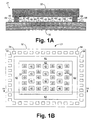
- Figs. 1A - 1C depict a micromachined structure 21 manufactured in accordance with the invention.
- Fig. 1A depicts a cross-sectional view of the structure 21 having a top micromachined wafer 25 and a base micromachined wafer 32.
- Fig. 1B depicts a top view of the wafer 32
- Fig. 1C depicts a bottom view of the wafer 25.
- the structure 21 is preferably designed to include contacts 42 in order to bond wafer 25 to wafer 32 and to maintain a position of wafer 25 with respect to wafer 32.
- wafer 32 may have circuitry 45 disposed thereon, which includes CMOS or other types of components.
- the circuitry 45 may define a medium for electrically or magnetically storing information.
- the top wafer 25 may include reading/writing elements 52 that read and write information to and from the media within circuitry 45.
- the location of the reading/writing elements 52 with respect to the media within circuitry 45 should be located at a particular position with respect to the media of circuitry 45 within precise tolerances. Accordingly, it may be desirable for the wafer 25 via contacts 42 to precisely maintain a particular position with respect to wafer 32.
- circuitry 45 and reading/writing elements 52 are not necessary for implementing the invention and are shown for illustrative purposes only.
- Figs. 1A and 1B show electrical contacts 58, which are also not necessary for implementing the invention. Electrical contacts 58 are preferably designed to provide an outside interface to the circuitry 45 in the preferred embodiment. In this regard, electrical connections connect each contact 58 to particular circuitry 45 within structure 21, although the connections are not shown by Figs. 1A and 1B for simplicity. Therefore, electrical signals can communicate between outside sources and the circuitry 45 within structure 21 via electrical contacts 58.
- the structure 21 is configured to include at least one column or contact 42, preferably comprising palladium (Pd).
- the contacts 42 are preferably formed on wafer 32 through normal micromachining techniques. Once formed on wafer 32, the contacts 42 are then bonded to the top wafer 25 in order to connect wafer 32 to wafer 25.
- top wafer 25 includes exposed silicon (Si), which can react with the palladium contact 42 during the bonding process to form a palladium-silicon bond between wafers 25 and 32.
- Si exposed silicon
- An example of a process of creating a palladium-silicon bond between two wafers is fully described in "System and Method for Bonding Wafers," filed by Merchant et al . on (to be determined) and assigned serial number (to be determined), which is incorporated herein by reference.
- the palladium contacts 42 are preferably attached to the base wafer 32 via an adhesion layer of chromium.
- the contacts 42 are configured to engage a silicon portion of wafer 25.
- a palladium-silicon (Pd-Si) bond forms between the palladium contacts 42 and the silicon of the wafer 25.
- the palladium contacts 42 may be bonded to silicon at temperatures less than approximately 450 degrees Celsius, the palladium-silicon bond between the two wafers can be formed without damaging any CMOS circuitry (or other components sensitive to temperatures above approximately 450 degrees Celsius) included within either of the two wafers 25 or 32. Therefore, the bonding process is compatible with CMOS circuitry, and wafers 25 and 32 may include CMOS components (or other components sensitive to temperatures above approximately 450 degrees Celsius) during the bonding process.
- structure 21 is preferably designed to include a gasket 62 for sealing the structure 21.
- the gasket 62 is configured to engage both wafers 25 and 32 and to enclose a portion of the space between wafer 25 and 32, as depicted by Figs. 1A and 1B.
- the space encompassed by gasket 62 and wafers 25 and 32 constitutes a chamber 63 within structure 21.
- Circuitry 45 preferably resides in this chamber 63 so that a vacuum, or other types of conditions, may be trapped and sealed around the circuitry 45, as will be discussed in more detail below.
- the material of the gasket 62 preferably is a soft pliable material. Furthermore, although other embodiments are possible, gasket 62 is preferably designed to engage wafer 25 before contacts 42 engage wafer 25, when the two wafers 25 and 32 are joined together. Therefore, in joining the two wafers 25 and 32, the gasket 62 is designed to engage the wafer 25 and to deform, due to a pressure that is exerted between the two wafers 25 and 32. Heating the joined wafers 25 and 32 forms the bond between contacts 42 and wafer 25, as discussed above, and fuses the gasket 62 to wafer 25. When the structure 21 is cooled, the fused material hardens to form a seal around a perimeter of the chamber 63. In this regard, the gasket 62 constitutes a side wall of the chamber 63. Therefore, the heating of the structure 21 not only forms the bond between the contacts 45 and the wafer 25, but it also seals the chamber 63.
- a germanium layer 65 is preferably formed on wafer 25 as depicted by Fig. 1C.
- the germanium layer 65 is configured to engage the gasket 62 when wafer 25 is engaged with wafer 32.
- the germanium layer 65 is configured to fuse with the gasket 62 during the bonding process and, therefore, to help form a sufficient seal for the structure 21.
- a sufficient seal is a seal capable of maintaining vacuum conditions within chamber 63.
- the material of the gasket 62 is preferably gold (Au). Therefore, when the gasket 62 is engaged with wafer 25 and heated, the surfaces of gasket 62 and wafer 25 engaged together form an eutectic which has a melting point close to or lower than the bonding temperature. If the germanium layer 65 is formed on wafer 25, then a gold-germanium (AuGe) eutectic is formed at the interface of the gasket 62 and layer 65. Otherwise, a gold-silicon (AuSi) eutectic is formed since the surface of wafer 25 is preferably silicon. When the eutectic cools and solidifies, a leak proof seal is formed between the wafers 25 and 32 by the hardened eutectic and gasket 62.
- AuGe gold-germanium
- AuSi gold-silicon
- the chamber 63 sealed by gasket 62 In many situations, it is desirable for the chamber 63 sealed by gasket 62 to be evacuated. In such a situation, the structure 21 should be placed in a vacuum chamber (not shown) while bonding of the two wafers 25 and 32 is performed. By engaging and heating the wafers 23 and 32, as discussed above, while the structure 21 is situated within an evacuated vacuum chamber, a vacuum is trapped and sealed within chamber 63. Therefore, in the preferred embodiment, the chamber 63 defined by the wafers 32 and 35 and the gasket 62 is designed to be evacuated.
- wafers 25 and 32 are manufactured through microfabrication techniques known in the art.
- wafer 25 preferably includes silicon on portions of its bottom surface, and the bottom surface of wafer 25 also includes a germanium layer 65, as depicted by Fig. 1C.
- contacts 42 preferably comprised of palladium, and a gasket 62, preferably comprised of gold, are formed on wafer 32 according to Figs. 1B and 2A.
- circuitry 45, reading/writing elements 52 and/or electrical connections 58 may be located on either side or on both sides of the perimeter defined by gasket 62.
- the wafers 25 and 32 are preferably placed into an annealing chamber which is then evacuated. Wafer 25 is then engaged with the gasket 62.
- gasket 62 is taller than contacts 42 such that wafer 25 engages gasket 62 prior to engaging any of the contacts 42.
- any configuration that allows a seal to form via gasket 62 when the structure 21 is heated during the bonding process is sufficient to implement the invention.
- the wafers 25 and 32 are pressed against one another.
- the structure 21 is then heated to a bonding temperature by increasing the temperature of the annealing chamber to the bonding temperature, as will be discussed in further detail.
- This bonding temperature is preferably below at least approximately 500 degrees Celsius so that any CMOS circuitry or other types of components included by either wafer 25 or 32 are not damaged.
- the surfaces of gasket 62 and wafer 25 i.e ., germanium layer 65 in the preferred embodiment
- engaged together form an eutectic.
- the palladium contacts 42 bond with the silicon in wafer 25 to form a palladium-silicon bond between wafers 25 and 32 and the eutectic melts.
- the temperature of the annealing chamber is then reduced in order to complete the bonding process of the palladium-silicon bond.
- the melted eutectic hardens or solidifies to form a seal between the gasket 62 and the wafer 25. Since the annealing chamber is evacuated, the formation of the seal creates a sealed vacuum in the chamber 63. Therefore, once the manufacturing process is complete, the structure 21 can be removed from the annealing chamber while preserving a vacuum sealed within the chamber 63.
- the temperature of the structure 21 is initially increased to approximately 200 degrees Celsius within about 30 seconds. Although not necessary, it is preferable to change the temperature linearly (i.e ., "ramp" the temperature) when the temperature of the structure 21 is being varied during the bonding process.
- the temperature of structure 21 is preferably held at approximately 200 degrees Celsius for about 30 seconds and then increased to the bonding temperature in about 15 seconds.
- bonding temperatures and durations sufficient for the invention are approximately 450 degrees Celsius for about 30 minutes, approximately 400 degrees Celsius for about 30 minutes, or approximately 300 degrees Celsius for about 45 minutes. It should be noted that other bonding temperatures and durations are possible for forming a sufficient bond between the palladium contacts 42 and wafer 23 and for fusing gold gasket 62 to wafer 25.
- the temperature of the structure 21 is decreased below approximately 100 degrees Celsius in about six minutes. At this point, a bond between contacts 42 and wafer 25 should be sufficient enough to keep wafer 21 attached and aligned to wafer 23 during normal operation within precise tolerances. Furthermore, the chamber 63 should be sealed by the wafers 32 and 35 and the gasket 62.
- the material of contacts 42, wafer 23 and gasket 62 are not necessarily pure palladium, pure silicon and pure gold, respectively.
- the preferred embodiment utilizes pure elements of palladium, silicon and gold, one ordinarily skilled in the art should realize that other elements can be added or combined with the silicon of wafer 25, the palladium contacts 42 and/or the gold gasket 62.
- the melting temperature of the sealing material should be close to the bonding temperature in order to achieve the benefit of forming a seal and a bond during the same heating process.
- utilizing the materials and the heating process described by the preferred embodiment enables the wafers 25 and 32 to be bonded and sealed with temperatures below approximately 450 degrees Celsius. Therefore, utilizing the materials and the heating process of the preferred embodiment enables structure 21 to be formed without damaging any CMOS circuitry or other types of temperature sensitive components included within wafers 25 and 32. Consequently, additional steps to preserve CMOS components or other types of temperature sensitive components are not necessary.
- CMOS components or other types of temperature sensitive components are not necessary.
- one skilled in the art should realize that other materials may be used to implement the invention, but the temperatures necessary to sufficiently bond the wafers 25 and 32 and/or to form the seal with gasket 62 may be affected.
- gasket 62 does not necessarily have to be formed on wafer 32 and engage wafer 25.
- gasket 62 may be formed on wafer 25 and engage wafer 32. Any configuration of gasket 62 is sufficient as long as a seal between wafer 25 and 32 is formed during the heating process.
Landscapes
- Micromachines (AREA)
- Measuring Fluid Pressure (AREA)
Applications Claiming Priority (2)
| Application Number | Priority Date | Filing Date | Title |
|---|---|---|---|
| US09/124,311 US6090687A (en) | 1998-07-29 | 1998-07-29 | System and method for bonding and sealing microfabricated wafers to form a single structure having a vacuum chamber therein |
| US124311 | 1998-07-29 |
Publications (3)
| Publication Number | Publication Date |
|---|---|
| EP0982773A2 EP0982773A2 (en) | 2000-03-01 |
| EP0982773A3 EP0982773A3 (en) | 2000-12-20 |
| EP0982773B1 true EP0982773B1 (en) | 2004-09-29 |
Family
ID=22414109
Family Applications (1)
| Application Number | Title | Priority Date | Filing Date |
|---|---|---|---|
| EP99105569A Expired - Lifetime EP0982773B1 (en) | 1998-07-29 | 1999-03-18 | System and method for bonding and sealing microfabricated wafers to form a single structure having a vacuum chamber therein |
Country Status (4)
| Country | Link |
|---|---|
| US (1) | US6090687A (enExample) |
| EP (1) | EP0982773B1 (enExample) |
| JP (1) | JP2000101019A (enExample) |
| DE (1) | DE69920606T2 (enExample) |
Families Citing this family (58)
| Publication number | Priority date | Publication date | Assignee | Title |
|---|---|---|---|---|
| US6287850B1 (en) * | 1995-06-07 | 2001-09-11 | Affymetrix, Inc. | Bioarray chip reaction apparatus and its manufacture |
| US6168963B1 (en) * | 1999-06-21 | 2001-01-02 | Lucent Technologies, Inc. | System for adhering parts |
| KR100343211B1 (ko) * | 1999-11-04 | 2002-07-10 | 윤종용 | 웨이퍼 레벨 진공 패키징이 가능한 mems의 구조물의제작방법 |
| US6669802B2 (en) * | 2000-12-21 | 2003-12-30 | Spenco | Composite riser |
| US6584416B2 (en) * | 2001-08-16 | 2003-06-24 | Hewlett-Packard Development Company | System and methods for forming data storage devices |
| DE10157848B4 (de) * | 2001-11-24 | 2005-01-13 | Eads Deutschland Gmbh | Verfahren zur Herstellung eines mikromechanischen Bauelements mit abgeschlossenem Innenraum und mikromechanisches Bauelement mit abgeschlossenem Innenraum |
| FR2834283B1 (fr) * | 2001-12-28 | 2005-06-24 | Commissariat Energie Atomique | Procede et zone de scellement entre deux substrats d'une microstructure |
| EP1535331B1 (en) * | 2002-03-19 | 2024-10-02 | Murata Integrated Passive Solutions | Method of forming a sealed cavity |
| US20040082058A1 (en) * | 2002-10-29 | 2004-04-29 | Arthur Schleifer | Array hybridization apparatus and method for making uniform sample volumes |
| US7275292B2 (en) * | 2003-03-07 | 2007-10-02 | Avago Technologies Wireless Ip (Singapore) Pte. Ltd. | Method for fabricating an acoustical resonator on a substrate |
| US20040214310A1 (en) * | 2003-04-25 | 2004-10-28 | Parker Russell A. | Apparatus and method for array alignment |
| DE10323394B4 (de) * | 2003-05-20 | 2006-09-28 | Fraunhofer-Gesellschaft zur Förderung der angewandten Forschung e.V. | Verfahren zum Erzeugen einer elektrischen Kontaktierung zwischen zwei Halbleiterstücken und Verfahren zum Herstellen einer Anordnung von Halbleiterstücken |
| US6946928B2 (en) * | 2003-10-30 | 2005-09-20 | Agilent Technologies, Inc. | Thin-film acoustically-coupled transformer |
| US7294919B2 (en) * | 2003-11-26 | 2007-11-13 | Avago Technologies General Ip (Singapore) Pte. Ltd. | Device having a complaint element pressed between substrates |
| US20050196761A1 (en) * | 2004-03-08 | 2005-09-08 | Thompson Allen C. | Array hybridization apparatus and method |
| US20050202445A1 (en) * | 2004-03-09 | 2005-09-15 | Thompson Allen C. | Thermoplastic array hybridization apparatus and method |
| US7615833B2 (en) * | 2004-07-13 | 2009-11-10 | Avago Technologies Wireless Ip (Singapore) Pte. Ltd. | Film bulk acoustic resonator package and method of fabricating same |
| US7388454B2 (en) | 2004-10-01 | 2008-06-17 | Avago Technologies Wireless Ip Pte Ltd | Acoustic resonator performance enhancement using alternating frame structure |
| US7274050B2 (en) * | 2004-10-29 | 2007-09-25 | Avago Technologies General Ip (Singapore) Pte. Ltd. | Packaging and manufacturing of an integrated circuit |
| US8981876B2 (en) | 2004-11-15 | 2015-03-17 | Avago Technologies General Ip (Singapore) Pte. Ltd. | Piezoelectric resonator structures and electrical filters having frame elements |
| DE102004056970B4 (de) * | 2004-11-25 | 2008-07-03 | Fraunhofer-Gesellschaft zur Förderung der angewandten Forschung e.V. | Verfahren und Vorrichtung zum Erzeugen einer elektrischen Kontaktierung zwischen zwei Halbleiterstücken durch ein mechanisches Element |
| US7202560B2 (en) | 2004-12-15 | 2007-04-10 | Avago Technologies Wireless Ip (Singapore) Pte. Ltd. | Wafer bonding of micro-electro mechanical systems to active circuitry |
| US7791434B2 (en) | 2004-12-22 | 2010-09-07 | Avago Technologies Wireless Ip (Singapore) Pte. Ltd. | Acoustic resonator performance enhancement using selective metal etch and having a trench in the piezoelectric |
| US7369013B2 (en) | 2005-04-06 | 2008-05-06 | Avago Technologies Wireless Ip Pte Ltd | Acoustic resonator performance enhancement using filled recessed region |
| US20070004079A1 (en) * | 2005-06-30 | 2007-01-04 | Geefay Frank S | Method for making contact through via contact to an offset contactor inside a cap for the wafer level packaging of FBAR chips |
| US7737807B2 (en) * | 2005-10-18 | 2010-06-15 | Avago Technologies Wireless Ip (Singapore) Pte. Ltd. | Acoustic galvanic isolator incorporating series-connected decoupled stacked bulk acoustic resonators |
| DE102006000687B4 (de) | 2006-01-03 | 2010-09-09 | Thallner, Erich, Dipl.-Ing. | Kombination aus einem Träger und einem Wafer, Vorrichtung zum Trennen der Kombination und Verfahren zur Handhabung eines Trägers und eines Wafers |
| US20070210748A1 (en) * | 2006-03-09 | 2007-09-13 | Mark Unkrich | Power supply and electronic device having integrated power supply |
| US7746677B2 (en) | 2006-03-09 | 2010-06-29 | Avago Technologies Wireless Ip (Singapore) Pte. Ltd. | AC-DC converter circuit and power supply |
| US7479685B2 (en) | 2006-03-10 | 2009-01-20 | Avago Technologies General Ip (Singapore) Pte. Ltd. | Electronic device on substrate with cavity and mitigated parasitic leakage path |
| US20080164606A1 (en) * | 2007-01-08 | 2008-07-10 | Christoffer Graae Greisen | Spacers for wafer bonding |
| US7732977B2 (en) | 2008-04-30 | 2010-06-08 | Avago Technologies Wireless Ip (Singapore) | Transceiver circuit for film bulk acoustic resonator (FBAR) transducers |
| US7855618B2 (en) | 2008-04-30 | 2010-12-21 | Avago Technologies Wireless Ip (Singapore) Pte. Ltd. | Bulk acoustic resonator electrical impedance transformers |
| US8058143B2 (en) * | 2009-01-21 | 2011-11-15 | Freescale Semiconductor, Inc. | Substrate bonding with metal germanium silicon material |
| US8202741B2 (en) * | 2009-03-04 | 2012-06-19 | Koninklijke Philips Electronics N.V. | Method of bonding a semiconductor device using a compliant bonding structure |
| EP2660851B1 (de) | 2009-03-18 | 2020-10-14 | EV Group GmbH | Vorrichtung und Verfahren zum Ablösen eines Wafers von einem Träger |
| US8902023B2 (en) | 2009-06-24 | 2014-12-02 | Avago Technologies General Ip (Singapore) Pte. Ltd. | Acoustic resonator structure having an electrode with a cantilevered portion |
| US8248185B2 (en) | 2009-06-24 | 2012-08-21 | Avago Technologies Wireless Ip (Singapore) Pte. Ltd. | Acoustic resonator structure comprising a bridge |
| EP2706561B1 (de) | 2009-09-01 | 2017-04-05 | EV Group GmbH | Verfahren zum konzentrischen Ablösen eines Produktsubstrats (z.B. eines Halbleiterwafers) von einem Trägersubstrat durch Verformung eines auf einem Filmrahmen montierten flexiblen Films |
| US8193877B2 (en) | 2009-11-30 | 2012-06-05 | Avago Technologies Wireless Ip (Singapore) Pte. Ltd. | Duplexer with negative phase shifting circuit |
| US9243316B2 (en) | 2010-01-22 | 2016-01-26 | Avago Technologies General Ip (Singapore) Pte. Ltd. | Method of fabricating piezoelectric material with selected c-axis orientation |
| US8796904B2 (en) | 2011-10-31 | 2014-08-05 | Avago Technologies General Ip (Singapore) Pte. Ltd. | Bulk acoustic resonator comprising piezoelectric layer and inverse piezoelectric layer |
| EP2523208B1 (de) | 2010-04-23 | 2013-06-12 | EV Group GmbH | Lösungsmittelbehälter und Verfahren zum Lösen einer Verbindungsschicht |
| JP6342033B2 (ja) * | 2010-06-30 | 2018-06-13 | キヤノン株式会社 | 固体撮像装置 |
| FR2963982B1 (fr) | 2010-08-20 | 2012-09-28 | Soitec Silicon On Insulator | Procede de collage a basse temperature |
| US8962443B2 (en) | 2011-01-31 | 2015-02-24 | Avago Technologies General Ip (Singapore) Pte. Ltd. | Semiconductor device having an airbridge and method of fabricating the same |
| US9425764B2 (en) | 2012-10-25 | 2016-08-23 | Avago Technologies General Ip (Singapore) Pte. Ltd. | Accoustic resonator having composite electrodes with integrated lateral features |
| US9154112B2 (en) | 2011-02-28 | 2015-10-06 | Avago Technologies General Ip (Singapore) Pte. Ltd. | Coupled resonator filter comprising a bridge |
| US9083302B2 (en) | 2011-02-28 | 2015-07-14 | Avago Technologies General Ip (Singapore) Pte. Ltd. | Stacked bulk acoustic resonator comprising a bridge and an acoustic reflector along a perimeter of the resonator |
| US9148117B2 (en) | 2011-02-28 | 2015-09-29 | Avago Technologies General Ip (Singapore) Pte. Ltd. | Coupled resonator filter comprising a bridge and frame elements |
| US9136818B2 (en) | 2011-02-28 | 2015-09-15 | Avago Technologies General Ip (Singapore) Pte. Ltd. | Stacked acoustic resonator comprising a bridge |
| US9048812B2 (en) | 2011-02-28 | 2015-06-02 | Avago Technologies General Ip (Singapore) Pte. Ltd. | Bulk acoustic wave resonator comprising bridge formed within piezoelectric layer |
| US9203374B2 (en) | 2011-02-28 | 2015-12-01 | Avago Technologies General Ip (Singapore) Pte. Ltd. | Film bulk acoustic resonator comprising a bridge |
| US9444426B2 (en) | 2012-10-25 | 2016-09-13 | Avago Technologies General Ip (Singapore) Pte. Ltd. | Accoustic resonator having integrated lateral feature and temperature compensation feature |
| US8575820B2 (en) | 2011-03-29 | 2013-11-05 | Avago Technologies General Ip (Singapore) Pte. Ltd. | Stacked bulk acoustic resonator |
| US8350445B1 (en) | 2011-06-16 | 2013-01-08 | Avago Technologies Wireless Ip (Singapore) Pte. Ltd. | Bulk acoustic resonator comprising non-piezoelectric layer and bridge |
| US8922302B2 (en) | 2011-08-24 | 2014-12-30 | Avago Technologies General Ip (Singapore) Pte. Ltd. | Acoustic resonator formed on a pedestal |
| JP5984912B2 (ja) * | 2012-03-23 | 2016-09-06 | オリンパス株式会社 | 積層型半導体の製造方法 |
Family Cites Families (6)
| Publication number | Priority date | Publication date | Assignee | Title |
|---|---|---|---|---|
| JPS5988864A (ja) * | 1982-11-12 | 1984-05-22 | Matsushita Electric Ind Co Ltd | 半導体装置の製造方法 |
| US4769272A (en) * | 1987-03-17 | 1988-09-06 | National Semiconductor Corporation | Ceramic lid hermetic seal package structure |
| US5262347A (en) * | 1991-08-14 | 1993-11-16 | Bell Communications Research, Inc. | Palladium welding of a semiconductor body |
| DE69321745T2 (de) * | 1992-02-04 | 1999-10-07 | Matsushita Electric Industrial Co., Ltd. | Direktkontakt-Bildsensor und Herstellungsverfahren dafür |
| JP3613838B2 (ja) * | 1995-05-18 | 2005-01-26 | 株式会社デンソー | 半導体装置の製造方法 |
| US5918794A (en) * | 1995-12-28 | 1999-07-06 | Lucent Technologies Inc. | Solder bonding of dense arrays of microminiature contact pads |
-
1998
- 1998-07-29 US US09/124,311 patent/US6090687A/en not_active Expired - Fee Related
-
1999
- 1999-03-18 EP EP99105569A patent/EP0982773B1/en not_active Expired - Lifetime
- 1999-03-18 DE DE69920606T patent/DE69920606T2/de not_active Expired - Fee Related
- 1999-07-28 JP JP11213164A patent/JP2000101019A/ja active Pending
Also Published As
| Publication number | Publication date |
|---|---|
| JP2000101019A (ja) | 2000-04-07 |
| EP0982773A3 (en) | 2000-12-20 |
| DE69920606T2 (de) | 2005-10-06 |
| DE69920606D1 (de) | 2004-11-04 |
| EP0982773A2 (en) | 2000-03-01 |
| US6090687A (en) | 2000-07-18 |
Similar Documents
| Publication | Publication Date | Title |
|---|---|---|
| EP0982773B1 (en) | System and method for bonding and sealing microfabricated wafers to form a single structure having a vacuum chamber therein | |
| US6400009B1 (en) | Hermatic firewall for MEMS packaging in flip-chip bonded geometry | |
| US7015074B2 (en) | Vacuum package fabrication of integrated circuit components | |
| US7132721B2 (en) | Bonding for a micro-electro-mechanical system (MEMS) and MEMS based devices | |
| US6118181A (en) | System and method for bonding wafers | |
| CN103904041A (zh) | 真空密封封装 | |
| US5801068A (en) | Hermetically sealed microelectronic device and method of forming same | |
| Welch et al. | Gold-indium transient liquid phase (TLP) wafer bonding for MEMS vacuum packaging | |
| US8138025B2 (en) | Microcap wafer bonding method and apparatus | |
| US4974769A (en) | Method of joining composite structures | |
| US20080134631A1 (en) | Airtight apparatus | |
| JP3648021B2 (ja) | 気密端子およびその形成方法 | |
| JP2003311400A (ja) | 通気孔を設けた空洞の気密はんだ封止法 | |
| JPH01244651A (ja) | セラミックパッケージ型半導体装置 | |
| JP3097770B2 (ja) | 封止体接続方法及び封止体 | |
| JP2845043B2 (ja) | 光ファイバ導入部の気密封止構造 | |
| JP3207020B2 (ja) | 光パッケージ | |
| JPS6259887B2 (enExample) | ||
| JPS5917270A (ja) | 半導体装置 | |
| JPS6329555A (ja) | 封止電子装置 | |
| WO2026048374A1 (ja) | リッド、デバイス、およびデバイスの製造方法 | |
| JPS5917542B2 (ja) | 半導体装置の気密封止組立方法 | |
| JPH10144828A (ja) | 半導体パッケージ | |
| JPH04321257A (ja) | 低融点ガラス封止型半導体装置 | |
| JPH03116855A (ja) | パッケージ構造 |
Legal Events
| Date | Code | Title | Description |
|---|---|---|---|
| PUAI | Public reference made under article 153(3) epc to a published international application that has entered the european phase |
Free format text: ORIGINAL CODE: 0009012 |
|
| AK | Designated contracting states |
Kind code of ref document: A2 Designated state(s): DE FR GB |
|
| AX | Request for extension of the european patent |
Free format text: AL;LT;LV;MK;RO;SI |
|
| PUAL | Search report despatched |
Free format text: ORIGINAL CODE: 0009013 |
|
| AK | Designated contracting states |
Kind code of ref document: A3 Designated state(s): AT BE CH CY DE DK ES FI FR GB GR IE IT LI LU MC NL PT SE |
|
| AX | Request for extension of the european patent |
Free format text: AL;LT;LV;MK;RO;SI |
|
| 17P | Request for examination filed |
Effective date: 20010228 |
|
| RAP1 | Party data changed (applicant data changed or rights of an application transferred) |
Owner name: HEWLETT-PACKARD COMPANY, A DELAWARE CORPORATION |
|
| RAP1 | Party data changed (applicant data changed or rights of an application transferred) |
Owner name: AGILENT TECHNOLOGIES INC. |
|
| RAP1 | Party data changed (applicant data changed or rights of an application transferred) |
Owner name: AGILENT TECHNOLOGIES INC. A DELAWARE CORPORATION |
|
| AKX | Designation fees paid |
Free format text: DE FR GB |
|
| RAP1 | Party data changed (applicant data changed or rights of an application transferred) |
Owner name: AGILENT TECHNOLOGIES, INC. (A DELAWARE CORPORATION |
|
| 17Q | First examination report despatched |
Effective date: 20020207 |
|
| GRAP | Despatch of communication of intention to grant a patent |
Free format text: ORIGINAL CODE: EPIDOSNIGR1 |
|
| GRAS | Grant fee paid |
Free format text: ORIGINAL CODE: EPIDOSNIGR3 |
|
| GRAA | (expected) grant |
Free format text: ORIGINAL CODE: 0009210 |
|
| AK | Designated contracting states |
Kind code of ref document: B1 Designated state(s): DE FR GB |
|
| REG | Reference to a national code |
Ref country code: GB Ref legal event code: FG4D |
|
| REF | Corresponds to: |
Ref document number: 69920606 Country of ref document: DE Date of ref document: 20041104 Kind code of ref document: P |
|
| PLBE | No opposition filed within time limit |
Free format text: ORIGINAL CODE: 0009261 |
|
| STAA | Information on the status of an ep patent application or granted ep patent |
Free format text: STATUS: NO OPPOSITION FILED WITHIN TIME LIMIT |
|
| ET | Fr: translation filed | ||
| 26N | No opposition filed |
Effective date: 20050630 |
|
| PGFP | Annual fee paid to national office [announced via postgrant information from national office to epo] |
Ref country code: DE Payment date: 20070430 Year of fee payment: 9 |
|
| PGFP | Annual fee paid to national office [announced via postgrant information from national office to epo] |
Ref country code: GB Payment date: 20070425 Year of fee payment: 9 |
|
| PGFP | Annual fee paid to national office [announced via postgrant information from national office to epo] |
Ref country code: FR Payment date: 20080311 Year of fee payment: 10 |
|
| GBPC | Gb: european patent ceased through non-payment of renewal fee |
Effective date: 20080318 |
|
| PG25 | Lapsed in a contracting state [announced via postgrant information from national office to epo] |
Ref country code: DE Free format text: LAPSE BECAUSE OF NON-PAYMENT OF DUE FEES Effective date: 20081001 |
|
| PG25 | Lapsed in a contracting state [announced via postgrant information from national office to epo] |
Ref country code: GB Free format text: LAPSE BECAUSE OF NON-PAYMENT OF DUE FEES Effective date: 20080318 |
|
| REG | Reference to a national code |
Ref country code: FR Ref legal event code: ST Effective date: 20091130 |
|
| PG25 | Lapsed in a contracting state [announced via postgrant information from national office to epo] |
Ref country code: FR Free format text: LAPSE BECAUSE OF NON-PAYMENT OF DUE FEES Effective date: 20091123 |