EP0977087B1 - Elektrophotographisches Gerät - Google Patents
Elektrophotographisches Gerät Download PDFInfo
- Publication number
- EP0977087B1 EP0977087B1 EP99114933A EP99114933A EP0977087B1 EP 0977087 B1 EP0977087 B1 EP 0977087B1 EP 99114933 A EP99114933 A EP 99114933A EP 99114933 A EP99114933 A EP 99114933A EP 0977087 B1 EP0977087 B1 EP 0977087B1
- Authority
- EP
- European Patent Office
- Prior art keywords
- substituted
- group
- unsubstituted
- unsubstituted aromatic
- charge
- Prior art date
- Legal status (The legal status is an assumption and is not a legal conclusion. Google has not performed a legal analysis and makes no representation as to the accuracy of the status listed.)
- Expired - Lifetime
Links
Images


Classifications
-
- G—PHYSICS
- G03—PHOTOGRAPHY; CINEMATOGRAPHY; ANALOGOUS TECHNIQUES USING WAVES OTHER THAN OPTICAL WAVES; ELECTROGRAPHY; HOLOGRAPHY
- G03G—ELECTROGRAPHY; ELECTROPHOTOGRAPHY; MAGNETOGRAPHY
- G03G5/00—Recording members for original recording by exposure, e.g. to light, to heat, to electrons; Manufacture thereof; Selection of materials therefor
- G03G5/02—Charge-receiving layers
- G03G5/04—Photoconductive layers; Charge-generation layers or charge-transporting layers; Additives therefor; Binders therefor
- G03G5/043—Photoconductive layers characterised by having two or more layers or characterised by their composite structure
- G03G5/047—Photoconductive layers characterised by having two or more layers or characterised by their composite structure characterised by the charge-generation layers or charge transport layers
-
- G—PHYSICS
- G03—PHOTOGRAPHY; CINEMATOGRAPHY; ANALOGOUS TECHNIQUES USING WAVES OTHER THAN OPTICAL WAVES; ELECTROGRAPHY; HOLOGRAPHY
- G03G—ELECTROGRAPHY; ELECTROPHOTOGRAPHY; MAGNETOGRAPHY
- G03G5/00—Recording members for original recording by exposure, e.g. to light, to heat, to electrons; Manufacture thereof; Selection of materials therefor
- G03G5/02—Charge-receiving layers
- G03G5/04—Photoconductive layers; Charge-generation layers or charge-transporting layers; Additives therefor; Binders therefor
- G03G5/06—Photoconductive layers; Charge-generation layers or charge-transporting layers; Additives therefor; Binders therefor characterised by the photoconductive material being organic
- G03G5/0601—Acyclic or carbocyclic compounds
- G03G5/0612—Acyclic or carbocyclic compounds containing nitrogen
- G03G5/0614—Amines
- G03G5/06142—Amines arylamine
- G03G5/06144—Amines arylamine diamine
- G03G5/061443—Amines arylamine diamine benzidine
-
- G—PHYSICS
- G03—PHOTOGRAPHY; CINEMATOGRAPHY; ANALOGOUS TECHNIQUES USING WAVES OTHER THAN OPTICAL WAVES; ELECTROGRAPHY; HOLOGRAPHY
- G03G—ELECTROGRAPHY; ELECTROPHOTOGRAPHY; MAGNETOGRAPHY
- G03G5/00—Recording members for original recording by exposure, e.g. to light, to heat, to electrons; Manufacture thereof; Selection of materials therefor
- G03G5/02—Charge-receiving layers
- G03G5/04—Photoconductive layers; Charge-generation layers or charge-transporting layers; Additives therefor; Binders therefor
- G03G5/06—Photoconductive layers; Charge-generation layers or charge-transporting layers; Additives therefor; Binders therefor characterised by the photoconductive material being organic
- G03G5/0601—Acyclic or carbocyclic compounds
- G03G5/0612—Acyclic or carbocyclic compounds containing nitrogen
- G03G5/0614—Amines
- G03G5/06142—Amines arylamine
- G03G5/06144—Amines arylamine diamine
- G03G5/061446—Amines arylamine diamine terphenyl-diamine
Definitions
- the present invention relates to an electrophotographic apparatus having a short-wavelength semiconductor laser as an exposure light source.
- Semiconductor lasers having oscillation wavelengths near 800 nm or 680 nm have been primarily used as laser light sources in electrophotographic apparatuses, such as laser printers.
- a variety of approaches for increasing resolution have been attempted to satisfy the requirements for high-quality output images.
- the shorter the oscillation wavelength of the laser the smaller the spot diameter of the laser. The smaller spot diameter enables formation of high-resolution latent images.
- One method is a combination of the use of a nonlinear optical material and second harmonic generation (SHG) to reduce the wavelength of the laser light to one-half, as disclosed in Japanese Patent Application Laid-Open Nos. 9-275242 , 9-189930 , and 5-313033 .
- SHG second harmonic generation
- the technology in this system as a primary light source has been established.
- This method generally uses GaAs semiconductor lasers and YAG lasers having high output which can prolong the service life of the apparatus.
- Another method is the use of a wide-gap semiconductor which facilitates miniaturization of an apparatus compared to a SHG device.
- Many wide-gap semiconductors have been researched in view of high luminous efficiency and include, for example, ZnSe semiconductor lasers disclosed in Japanese Patent Application Laid-Open Nos. 7-32409 and 6-334272 and GaN semiconductor lasers disclosed in Japanese Patent Application Laid-Open Nos. 8-88441 and 7-335975 .
- the most usable semiconductor laser is a GaN semiconductor laser which sustains 1,150 hours of continuous oscillation at 50°C (disclosed in October 1997), as a result of technical innovation.
- Conventional laser electrophotographic photosensitive members used in electrophotographic apparatuses are designed so as to have practical levels of sensitivity to a long-wavelength region of approximately 700 to 800 nm.
- These electrophotographic photosensitive members use charge generation materials, such as nonmetal phthalocyanines and metal phthalocyanines, e.g., copper phthalocyanine and oxytitanium phthalocyanine, which do not have absorption bands at 400 to 500 nm.
- charge generation materials such as nonmetal phthalocyanines and metal phthalocyanines, e.g., copper phthalocyanine and oxytitanium phthalocyanine, which do not have absorption bands at 400 to 500 nm.
- these electrophotographic photosensitive members do not have practical levels of sensitivity to a wavelength region of 400 to 500 nm due to insufficient generation of carriers.
- a charge-generating material having a sufficient absorption band at 400 to 500 nm does not always achieve sufficiently high sensitivity.
- generation of charged carriers and transfer of the charged carriers are performed by different layers in order to achieve high sensitivity.
- a photosensitive member having a charge-generating layer and a charge transport layer deposited on a conductive substrate in that order exposure is performed when laser light passes through the charge transport layer and reaches the charge-generating layer.
- the charge transport layer is composed of a charge transfer material having a large absorption coefficient at a short wavelength of 400 to 500 nm, the light does not sufficiently reach the charge-generating layer. Accordingly, the use of the charge-generating material having high absorption at 400 to 400 nm does not show high sensitivity.
- short wavelength light may cause degradation or isomerization of the charge transfer material and thus cause deterioration of the charge transfer material during repeated use, even if the charge transport layer passes through the short-wavelength light of 400 to 500 nm.
- US-A-5 376 487 discloses a laminated-type photosensitive member having a photosensitive layer comprising a charge generating layer and a charge transporting layer having a layer thickness of 25 ⁇ m or more and containing a specific arylamine compound as a charge transporting material and an electron-accepting compound having an electron-affinity of 0.85-1.0 eV on an electrically conductive substrate.
- the maximal absorption wavelength of a charge-transfer complex of the arylamine compound with the electron-accepting compound is in the range of 480-550 nm.
- EP-A-0 435 165 discloses an electrophotographic photoreceptor comprising an electrically conductive support and a photosensitive layer formed thereon, wherein said photosensitive layer contains a specific arylamine compound.
- It is another object of the present invention to provide an electrophotographic apparatus comprising an electrophotographic photosensitive member having high sensitivity to a wavelength region of 380 to 450 nm and having a reduced change in potential during repeated use, and a short-wavelength laser and capable of continuously outputting high-quality images.
- a first aspect of the present invention is the use of an electrophotographic photosensitive member according to claim 4.
- a further aspect of the present invention is an electrophotographic apparatus as defined in claim 1.
- the electrophotographic photosensitive member in accordance with the present invention is irradiated with semiconductor laser light having a wavelength in a range of 380 to 450 nm, and has a charge transport layer which has a transmittance of at least 90 % for the semiconductor laser light.
- Figs. 1 to 4 are cross-sectional views of exemplary layer configurations in a layered electrophotographic photosensitive member having a conductive substrate, a charge-generating layer formed thereon and a charge transport layer formed thereon.
- the electrophotographic photosensitive member includes a conductive substrate 1, a charge-generating layer 2 formed thereon, and a charge transport layer formed thereon.
- the electrophotographic photosensitive member further includes an underlying layer 4 formed on the conductive substrate, in addition to the layers shown in Fig. 1.
- the electrophotographic photosensitive member further includes a protective layer 5 formed on the charge transport layer 3, in addition to the layers shown in Fig. 1.
- the electrophotographic photosensitive member further includes the underlying layer 2 and the protective layer 5. Any other configuration may be employed in the present invention.
- charge-generating materials preferably used in the present invention. These charge-generating materials may be used alone or in combination.
- the charge-generating layer containing a charge-generating material is preferably formed by dispersing the charge-generating material into a proper binder and coating the dispersion onto a conductive substrate. Alternatively, it may be formed on a conductive substrate by a dry process such as a deposition, sputtering or CVD process.
- the binder can be selected from a variety of binding resins.
- binding resins include polycarbonate resins, polyester resins, polyarylate resins, butyral resins, polystyrene resins, polyvinylacetal resins, diallyl phthalate resins, acrylic resins, methacrylic resins, vinyl acetate resins, phenol resins, silicone resins, polysulfone resins, styrene-butadiene copolymeric resins, alkyd resins, epoxy resins, urea resins, and vinyl chloride-vinyl acetate copolymeric resins. These resins may be used alone or in combination.
- the charge-generating layer preferably contains the binding resin in an amount of 80 percent by weight or less and more preferably 40 percent by weight or less.
- the thickness of the charge-generating layer is preferably 5 ⁇ m or less and more preferably in a range of 0.01 ⁇ m to 2 ⁇ m.
- the charge-generating layer may contain a variety of sensitizers.
- the charge transport layer containing a charge transfer material has a transmittance of at least 90% for radiated laser light.
- the charge transport layer is formed of a combination of a charge transfer material and one of the above-mentioned binding resins. Further binding resins suitable for the charge transport layer are conductive polymers, such as polyvinylcarbazole and polyvinylanthracene.
- the charge transfer materials are classified into electron transport materials and hole transport materials.
- electron transport materials include electrophilic materials, such as 2,4,7-trinitrofluorenone, 2,4,5,7-tetranitrofluorenone, chloranil and tetracyanoquinodimethane, and polymers of the electrophilic materials.
- hole transport materials include polycyclic aromatic compounds, such as pyrene and anthracene; heterocyclic compounds, such as carbazoles, indoles, oxazoles, thiazoles, oxadiazoles, pyrazoles, pyrazolines, thiadiazoles, and triazoles; miscellaneous compounds, such as hydrazones, styryls, benzidines, triarylmethanes, and triarylamines; and polymers having groups derived from these compounds in main or side chains, such as poly-N-vinylcarbazole and polyvinylanthracene. These charge transfer materials may be used alone or in combination.
- a large variation in potential on the photosensitive member after repeated use and image defects, including ghosting, are noticeable in a combination of a photosensitive member using a charge-generating material having a sufficient absorption band at approximately 400 nm to 500 nm and a light source emitting light having a wavelength of approximately 400 nm, rather than a combination of a conventional photosensitive member for a longer wavelength and a light source for a longer wavelength.
- One factor causing such phenomena is partial accumulation of excitons and charged carriers, which are generated by irradiation of short-wavelength light having high energy and are not consumed during the electrophotographic process. Such accumulation will change charging characteristics and sensitivity of the photosensitive member.
- the present inventors have discovered that accumulation of the excitons and carriers can be suppressed by electron transfer reaction with a charge transfer material which can suppress a change in potential and a memory phenomenon during repeated use and can form stable high-quality images.
- electrophotographic photosensitive members Since printers provided with electrophotographic photosensitive members are used in various fields, the electrophotographic photosensitive members are designed so as to provide stable images in various environments.
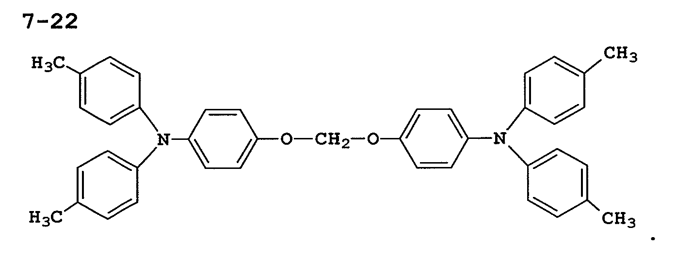
- the charge transfer materials used in the present invention are represented by the following formulae (1) to (7): wherein Ar 1-1 , Ar 1-2 and Ar 1-3 each is a substituted or unsubstituted aromatic group.
- unsubstituted aromatic groups include aryl groups, e.g., phenyl, naphthyl, anthracenyl and pyrenyl; aromatic heterocyclic groups, e.g., pyridyl, quinolyl, thienyl, furyl, benzimidazolyl and benzothiazolyl.
- substituent groups in the substituted aromatic groups include alkyl groups, e.g., methyl, ethyl, propyl, butyl and hexyl; alkoxy groups, e.g., methoxy, ethoxy and butoxy; halogen atoms, e.g., fluorine, chorine and bromine; aralkyl groups, e.g., benzyl, phenethyl, naphthylmethyl, and furfuryl; acyl groups, e.g., acetyl and benzyl; haloalkyl groups, e.g., trifluoromethyl; cyano groups; nitro groups; phenylcarbamoyl groups; carboxy groups; and hydroxy groups.
- alkyl groups e.g., methyl, ethyl, propyl, butyl and hexyl
- alkoxy groups e.g., methoxy, eth
- Ar 2-1 is a substituted or unsubstituted aromatic groups
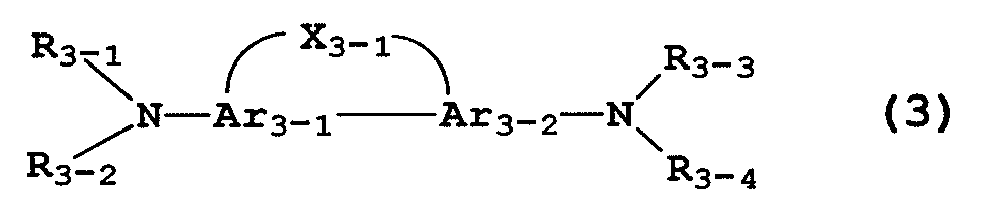
- Ar 2-2 , Ar 2-3 , Ar 3-1 and Ar 3-2 each is a substituted or unsubstituted aromatic group.
- R 2-1 to R 3-4 each is a substituted or unsubstituted alkyl group, a substituted or unsubstituted aralkyl group, a substituted or unsubstituted vinyl group, or a substituted or unsubstituted aromatic group, wherein at least two of R 3-1 to R 3-4 are the substituted or unsubstituted aromatic groups.
- Ar 4-1 and Ar 4-3 each is a substituted or unsubstituted aromatic group
- Ar 4-2 is a substituted or unsubstituted aromatic group
- R 4-1 is a substituted or unsubstituted alkyl group, a substituted or unsubstituted aralkyl group, a substituted or unsubstituted vinyl group, or a substituted or unsubstituted aromatic group.
- examples of unsubstituted aromatic groups of R 2-1 , Ar 2-1 , R 3-1 to R 3-4 , R 4-1 , Ar 4-1 and Ar 4-3 include aryl groups, e.g., phenyl, naphthyl, anthracenyl and pyrenyl; aromatic heterocyclic groups, e.g., pyridyl, quinolyl, thienyl, furyl, carbazolyl, benzimidazolyl and benzothiazolyl.
- aromatic groups of Ar 2-2 , Ar 2-3 , Ar 3-1 , Ar 3-2 and Ar 4-2 include divalent and trivalent residues (two or three hydrogen atoms are omitted) of aromatic compounds, such as benzene, naphthalene, anthracene and pyrene, and aromatic heterocyclic compounds, such as pyridine, quinoline, thiophene and furan.
- alkyl groups include methyl, ethyl, propyl, butyl and hexyl.
- aralkyl groups include benzyl, phenetyl, naphthylmethyl and furfuryl.
- substituent groups in these substituted groups include alkyl groups, e.g.
- alkoxy groups e.g., methoxy, ethoxy and butoxy
- halogen atoms e.g., fluorine, chorine and bromine
- aryl groups e.g., phenyl and naphthyl
- aromatic heterocyclic groups e.g., pyridyl, quinolyl, thienyl and furyl
- acyl groups e.g., acetyl and benzyl
- haloalkyl groups e.g., trifluoromethyl
- cyano groups nitro groups
- phenylcarbamoyl groups carboxy groups
- hydroxy groups e.g., trifluoromethyl
- Ar 5-1 and Ar 5-2 each is a substituted or unsubstituted aromatic group.
- R 5-1 to R 5-4 each is a substituted or unsubstituted alkyl group, a substituted or unsubstituted aralkyl group, a substituted or unsubstituted vinyl group, or a substituted or unsubstituted aromatic group, wherein at least two of R 5-1 to R 5-4 are the substituted or unsubstituted aromatic groups.
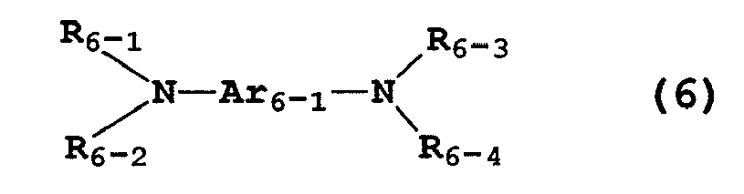
- Ar 6-1 is a substituted or unsubstituted aromatic group.
- R 6-1 to R 6-4 each is a substituted or unsubstituted alkyl group, a substituted or unsubstituted aralkyl group, a substituted or unsubstituted vinyl group, or a substituted or unsubstituted aromatic group, wherein at least two of R 6-1 to R 6-4 are the substituted or unsubstituted aromatic groups.
- Ar 7-1 and Ar 7-2 each is a substituted or unsubstituted aromatic group.
- R 7-1 to R 7-4 each is a substituted or unsubstituted alkyl group, a substituted or unsubstituted aralkyl group, a substituted or unsubstituted vinyl group, or a substituted or unsubstituted aromatic group, wherein at least two of R 7-1 to R 7-4 are the substituted or unsubstituted aromatic groups.
- X 7-1 is a divalent organic group and preferably -CR 6 R 7 -(wherein R 6 and R 7 each is hydrogen, a substituted or unsubstituted alkyl group, a substituted or unsubstituted alkoxy group, a substituted or unsubstituted aralkyl group, a substituted or unsubstituted aromatic group wherein R 6 to R 7 may form a ring), -O-, -S-, -CH 2 -O-CH 2 -, -O-CH 2 -O-, -NR 8 -(wherein R 8 is a substituted or unsubstituted alkyl group or a substituted or unsubstituted aromatic group), or a substituted or unsubstituted arylene group.
- examples of unsubstituted aromatic groups of R 5-1 to R 5-4 , R 6-1 to R 6-4 and R 7-1 to R 7-4 include aryl groups, e.g., phenyl, naphthyl, anthracenyl and pyrenyl; aromatic heterocyclic groups, e.g., pyridyl, quinolyl, thienyl, furyl, carbazolyl, benzimidazolyl and benzothiazolyl. Examples of aromatic groups of Ar 5-1 , Ar 5-2 .
- Ar 6-1, Ar 7-1 and Ar 7-2 include divalent residues (two hydrogen atoms are omitted) of aromatic compounds, such as benzene, naphthalene, anthracene and pyrene, and aromatic heterocyclic compounds, such as pyridine, quinoline; thiophene and furan.
- alkyl groups include methyl, ethyl, propyl, butyl and hexyl.
- Examples of aralkyl groups include benzyl, phenetyl, naphthylmethyl and furfuryl.
- alkoxy groups include methoxy and ethoxy.
- substituent groups in these substituted groups include alkyl groups, e.g., methyl, ethyl, propyl, butyl and hexyl; alkoxy groups, e.g., methoxy, ethoxy and butoxy; halogen atoms, e.g., fluorine, chorine and bromine; aryl groups, e.g., phenyl and naphthyl; aromatic heterocyclic groups, e.g., pyridyl, quinolyl, thienyl and furyl; acyl groups, e.g., acetyl and benzyl; haloalkyl groups, e.g., trifluoromethyl; cyano groups; nitro groups; phenylcarbamoyl groups; carboxy groups; and hydroxy groups.
- alkyl groups e.g., methyl, ethyl, propyl, butyl and hexyl
- the charge transfer material is preferably compounded in an amount of 10 to 500 parts by weight to 100 parts by weight of the binder.
- the charge transport layer is electrically conducted to the charge-generating layer, receives carriers injected from the charge-generating layer under an electric field, and transports the carriers to the surface.
- the thickness of the charge transport layer is in a range of preferably 5 ⁇ m to 40 ⁇ m and more preferably 10 ⁇ m to 30 ⁇ m, in consideration of transportability of charged carriers.
- the charge transport layer may contain antioxidant, UV absorbent and plasticizers, if necessary.
- Materials for the underlying layer optionally formed in the present invention includes casein, polyvinyl alcohol, nitrocellulose, polyamide, e.g., nylon-6, nylon-6,6, nylon-10, and compolymeric nylon, polyurethanes, and aluminum oxide.
- the thickness of the underlying layer is in a range of preferably 0.1 ⁇ m to 10 ⁇ m and more preferably 0.5 to 5 ⁇ m.
- the protective layer optionally formed on the photosensitive layer in the present invention may be a resinous layer.
- the resinous layer may contain conductive particles.
- These layers may be formed by any coating process using a solvent.
- the coating processes include a dip coating process, a spray coating process, a spin coating process, a roller coating process, a Meyer bar coating process, and a blade coating process.
- the exposure means in the present invention has a semiconductor laser having an oscillation wavelength of 380 nm to 450 nm as an exposure light source.
- Other configurations are not limited in the present invention. It is more preferable in view of a wide variety of selectivity of charge transfer materials and facility cost that the oscillation wavelength be in a range of 400 nm to 450 nm.
- any charging means, any developing means, any transfer means and any cleaning means may be employed without restrictions.
- Fig. 5 is a schematic cross-sectional view of an electrophotographic apparatus having a process cartridge provided with the photosensitive member of the present invention.
- a drum electrophotographic photosensitive member 6 turns on an axis 7 in the direction of the arrow in the drawing.
- the photosensitive member 6 is uniformly charged to a given negative or positive potential by a primary charging means 8, and is then exposed by exposure light 9 from an exposure means (not shown in the drawing) by, for example, laser beam scanning.
- a latent image is formed on the surface of the photosensitive member 6 sequentially.
- the latent image is developed by a develop means 10 with toner, and the developed toner image on the photosensitive member 6 is transferred onto a recording sheet 12 fed from a feeder (not shown in the drawing) to a gap between the photosensitive member 6 and a transfer means 11 in synchronism with the rotation of the photosensitive member 6.
- the recording sheet 12 is detached from the photosensitive member 6, is introduced to a fixing means 13 to fix the transferred image and is discharged from the apparatus.
- the residual toner on the surface of the photosensitive member 6 is removed after the transfer by a cleaning means 14.
- the surface of the photosensitive member 6 is deelectrified and then is used in the subsequent image formation. Since the primary charging means 8 in the drawing is a contact-type charging means using a charging roller, preliminary exposure is not always necessary.
- At least two components among the electrophotographic photosensitive member 6, the primary charging means 8, the developing means 10 and the cleaning means 14 may be integrally combined as a process cartridge which is attachable to and detachable from an electrophotographic apparatus body, such as a copying machine or a laser beam printer.
- a process cartridge 16 includes the photosensitive member 6 and at least one of the components of the primary charging means 8, the developing means 10 and the cleaning means 14, and is attachable to and detachable from the apparatus body by a guide means such as a rail 17.
- a coating solution of 5.5 parts of N-methoxylated nylon-6 (weight average molecular weight: 30,000) and 8 parts of alcohol-soluble copolymeric nylon (weight average molecular weight: 28,000) in a mixed solvent of 30 parts of methanol and 80 parts of butanol was coated on an aluminum substrate using a Meyer bar, and was then dried to form an underlying layer having a thickness of approximately 1 ⁇ m.
- a charge transport layer solution was prepared by dissolving 7 parts of Compound 1-6 and 10 parts of bisphenol-Z type polycarbonate (weight average molecular weight: 45,000) in 60 parts of monochlorobenzene. The solution was coated on the charge-generating layer using a Meyer bar, and dried at 100°C for one hour to form a charge transport layer having a thickness of approximately 23 ⁇ m. An electrophotographic photosensitive member was thereby formed.
- the electrophotographic characteristics of the resulting photosensitive member were measured using an electrostatic copying sheet tester EPA-8100 made by Kawaguchi Electric Co., Ltd.
- the photosensitive member was charged to a surface potential of -600 volts using a Corona charger, and was exposed with a monochromatic light beam of 380 nm from a monochromator.
- the dose when the surface potential is decreased to -300 volts was measured to determine a half-exposure sensitivity E 1/2 .
- a residual surface potential V r after exposure for 30 seconds was determined.
- the initial dark potential (V d ) and the initial light potential (V l ) were set to be approximately -600 volts and -200 volts, respectively, at ordinary temperature (23°C) and ordinary humidity (55%RH), wherein the dark potential means a potential at a dark portion and the light potential means a potential at a light portion.
- Charging and exposure cycles were repeated 5,000 times using a monochromic light beam of 380 nm to measure changes ( ⁇ V d and ⁇ V l ) in V d and V l .
- the negative sign in the change in the potential means a decrease in absolute value of the potential, whereas the positive sign means an increase in absolute value of the potential.
- Fig. 6 shows transmission spectra, wherein numerals in the drawing represents the identification numbers of the compounds.
- Electrophotographic photosensitive members were prepared and evaluated as in Example 1 using the compounds shown in Table 1 instead of Compound 1-6. The results are also shown in Table 1 and Fig. 6.
- Electrophotographic photosensitive members were prepared and evaluated as in Example 1 using the compounds represented by the following formulae, instead of Compound 1-6. The results are also shown in Table 1.
- the electrophotographic photosensitive members of the present invention have high sensitivity to exposure light of approximately 380 nm, and show high stability in potential and sensitivity after repeated use.
- An electrophotographic photosensitive member having a charge transport layer having a high transmittance is preferable in view of high sensitivity.
- the photosensitive members of Comparative Examples 1 and 2 having electron transport layers which do not transmit the 380-nm light do not have sensitivity.
- Electrophotographic photosensitive members were prepared as in Example 1 using the compounds shown in Table 2 instead of Compound 1-6. Electrophotographic characteristics of the resulting photosensitive members were evaluated as in Example 1 using a monochromatic light beam of 445 nm instead. The results are shown in Table 2 and Fig. 6.
- the photosensitive member using Compound 1-11 shows a high transmittance and high sensitivity at 445 nm, as shown in Example 9, whereas it shows a low transmittance and low sensitivity at 380 nm as shown in Example 5.
- Electrophotographic photosensitive members were prepared as in Example 1 using the compounds shown in Table 3 instead of Compound 1-6. Electrophotographic characteristics of the resulting photosensitive members were evaluated as in Example 1 using a monochromatic light beam of 500 nm instead. The results are shown in Table 3.
- Table 3 Compound for Charge Transfer Material Transmittance % (500 nm) Initial Characteristics Repetition Characteristics E 1/2 ( ⁇ J/cm 2 ) Vr (-V) ⁇ V d ⁇ V l
- Example 11 1-9 100 0.47 0 -20 0
- Example 13 1-33 100 0.50 5 -20 0
- a conductive layer coating was prepared by dispersing 50 parts of powdered titanium oxide covered with tin oxide containing 10% antimony oxide, 25 parts of a resol-type phenolic resin, 20 parts of methyl cellosolve, 5 parts of methanol, 0.002 parts of silicon oil (polydimethylsiloxane-polyoxyalkylene copolymer, average molecular weight: 3,000) in a sand mill using 1-mm diameter glass beads.
- the coating was dip-coated on an aluminum cylinder (30 mm diameterx251 mm) and dried at 140°C for 30 minutes to form a conductive layer having a thickness of 20 ⁇ m.
- An underlayer solution was prepared by dissolving 5 parts of N-methoxylated nylon-6 (weight average molecular weight: 52,000) and 10 parts of alcohol-soluble copolymeric nylon (weight average molecular weight: 48,000) into 95 parts of methanol.
- the underlayer solution was dip-coated on the conductive layer and dried to form an underlying layer having a thickness of 0.8 ⁇ m.
- a charge transport layer solution was prepared by dissolving 8 parts of each of the compounds shown in Table 4 and 10 parts of bisphenol-Z type polycarbonate (weight average molecular weight: 45,000) in 65 parts of monochlorobenzene. The solution was coated on the charge-generating layer using a Meyer bar, and dried at 100°C for one hour to form a charge transport layer having a thickness of approximately 21 ⁇ m. Electrophotographic photosensitive members of Examples 14 and 15 were thereby formed.
- Each of the electrophotographic photosensitive members was mounted in a modified printer LBP-2000 made by Canon Kabusiki Kaisha having a pulse modulator.
- the printer had a solid-state blue SHG laser ICD-430 made by Hitachi Metal, Ltd., as a light source (oscillation wavelength: 430 nm), and was modified to a Carlson-type electrophotographic system (reversal developing) including charging-exposure-developing-transfer-cleaning and responding to 600 dpi images.
- the dark potential V d was set to be -650 volts
- the light potential V l was set to be -200 volts
- an image which includes a checkerboard pattern (alternatively on/off pattern) and five-point characters was output. The resulting image was visually evaluated. The results are shown in Table 4.
- Example 14 An image from the photosensitive member used in Example 14 was evaluated as in Example 14, except that a GaAs semiconductor laser having an oscillation wavelength of 780 nm was used as a light source of the printer. The results are also shown in Table 4.
- Table 4 The results in Table 4 show that the electrophotographic apparatus of the present invention has high reproducibility of dots and characters and can output high-resolution images.
- Table 4 Compound for Charge Transfer Material Laser Oscillation wavelength Dot Reproducibility Character Reproducibility Example 14 1-9 430 nm Clear Clear Example 15 1-10 430 nm Clear Clear Comparative Example 7 1-9 780 nm Not reproduced Unclear (tailing in sub-scanning direction)
- Electrophotographic photosensitive members were prepared as in Example 1 using the compounds shown in Table 5 instead of Compounds 1-6 in Example 1, changing the thickness of the charge-generating layer to approximately 0.2 ⁇ m, and changing the thickness of the charge transport layer to 25 ⁇ m. All charge transport layers of these photosensitive members had transmittances of 30% or more to 450-nm light. For example, the charge transport layer of Example 20 had a transmittance of 100%.
- Electrophotographic characteristics of each photosensitive member was measured using an electrostatic copying sheet tester EPA-8100 made by Kawaguchi Electric Co., Ltd.
- the photosensitive member was charged to a surface potential of -700 volts using a Corona charger, and was exposed with a monochromatic light beam of 450 nm from a monochromator.
- the dose when the surface potential is decreased to -350 volts was measured to determine a half-exposure sensitivity E 1/2 .
- a residual surface potential V r after exposure for 30 seconds was determined.
- the initial dark potential (V d ) and the initial light potential (V l ) were set to be approximately -700 volts and -200 volts, respectively, at ordinary temperature (23°C) and ordinary humidity (55%RH). Charging and exposure cycles were repeated 5,000 times using a monochromic light beam of 450 nm to measure changes ( ⁇ V d and ⁇ V l ) in V d and V l .
- the environment was changed to a high-temperature, high-humid environment (33°C and 85% RH) to measure a change in V l from that in normal temperature and normal humidity.
- the negative sign in the change in the potential means a decrease in absolute value of the potential, whereas the positive sign means an increase in absolute value of the potential.
- the initial dark potential (V d ) and the initial light potential (V l ) for a monochromatic light beam of 450 nm were set to be approximately -700 volts and -200 volts, respectively.
- the photosensitive member was partly irradiated with a monochromic light beam of 450 nm having an intensity of 20 ⁇ W/cm 2 for 20 minutes, and V d and V l of the photosensitive member were measured to determine the difference ⁇ V d in the dark potential between the irradiated portion and the unirradiated portion and the difference ⁇ V l in the light potential between the irradiated portion and the unirradiated portion.
- the negative sign in the potential difference means that the potential at the irradiated portion is lower than that at the nonirradiated portion, and the positive sign means the reverse thereof.
- An electrophotographic photosensitive member was prepared and evaluated as in Example 16 using Compound A represented by the following formula instead of Compound 1-7. The results are also shown in Table 5.
- the charge transport layer of this photosensitive member had a transmittance of in a range of 30% to less than 90%.
- An electrophotographic photosensitive member was prepared and evaluated as in Example 16 using Compound B represented by the following formula instead of Compound 1-7. The results are also shown in Table 5.
- the charge transport layer of this photosensitive member had a transmittance of in a range of 30% to less than 90%.
- Electrophotographic photosensitive members were prepared and evaluated as in Example 16 using the compounds shown in Table 6 instead of Compound 1-7. The results are shown in Table 6. The charge transport layers of these photosensitive members had transmittances of at least 30%.
- Electrophotographic photosensitive members were prepared and evaluated as in Example 16 using the compound represented by the following formula instead of the azo compound and using the compounds shown in Table 7 instead of Compound 1-7. The results are shown in Table 7.
- Electrophotographic photosensitive members were prepared and evaluated as in Example 30 using the compounds shown in Table 8 instead of Compound 2-5. The results are shown in Table 8.
- Table 6 Example Compound for Charge Transfer Material Initial Characteristics Repetition Characteristics Environmental Characteristic Optical Memory E 1/2 ( ⁇ J/cm 2 ) Vr (-V) ⁇ V d (V) ⁇ V l (V) ⁇ V l (V) ⁇ V d (V) ⁇ V l (V) Example 26 4-8 0.42 5 -20 -20 5 -30 -20 Example 27 4-9 0.49 10 -25 -25 10 -30 -25 Example 28 4-16 0.46 10 -25 -25 5 -25 -20 Example 29 4-20 0.50 15 -30 -25 15 -35 -35 Table 7
- electrophotographic photosensitive members using the compounds represented by the formulae (1) to (4) have high sensitivity to short-wavelength exposure light, high stability of potential and sensitivity after repeated use, a low level of environmental dependence, and a low level of optical memory to short-wavelength light.
- Electrophotographic photosensitive members were prepared as in Example 14, except that charge-generating layers and charge transport layers were formed as follows.
- a charge transport layer solution was prepared by dissolving 9 parts of each of compounds shown in Table 4 and 10 parts of bisphenol-Z type polycarbonate (weight average molecular weight: 45,000) in 65 parts of monochlorobenzene. The solution was dip-coated on the charge-generating layer, and dried at 100°C for one hour to form a charge transport layer having a thickness of approximately 22 ⁇ m. Electrophotographic photosensitive members of Examples 37 and 43 were thereby formed.
- Each of the electrophotographic photosensitive members was mounted in a modified printer LBP-2000 made by Canon Kabusiki Kaisha having a pulse modulator and was evaluated.
- the printer had a solid-state blue SHG laser ICD-430 made by Hitachi Metal, Ltd., as a light source (oscillation wavelength: 430 nm), and was modified to a Carlson-type electrophotographic system (reversal developing) including charging-exposure-developing-transfer-cleaning and responding to 600 dpi images.
- the initial dark potential (V d ) and the initial light potential (V l ) were set to be approximately -650 volts and -200 volts, respectively, and an image including a checkerboard pattern (alternatively on/off pattern) and five-point characters was output. The resulting image was visually evaluated. The results are shown in Table 9, wherein “A” indicates “Excellent”, “B” indicates “Good”, “C” indicates “Average”, and "D” indicates "Not Good”.
- a character pattern corresponding to one turn of the drum was printed at normal temperature (23°C) and normal humidity (55% RH) to visually observe occurrence of the ghosting phenomenon.
- a pattern for checking durability 5,000 continuous printing operations were performed. This pattern included vertical and horizontal lines with a width of approximately 2 mm at a distance of 7 mm. Then, an entire black image and a checkerboard pattern (alternatively on/off pattern) and five-point characters were printed to check for the occurrence of the ghosting phenomenon, while changing the developing volume of the machine to F5 (intermediate value) and F9 (high concentration).
- Rank 5 indicates “No ghosting”
- Rank 4 indicates “ghosting is observed in the checkerboard pattern at F9”
- Rank 3 indicates “ghosting is observed in the checkerboard pattern at F5"
- Rank 2 indicates “ghosting is observed in the entire black pattern at F9”
- Rank 1 indicates "ghosting is observed in the entire black pattern at F5".
- An electrophotographic photosensitive member was prepared as in Example 37, using the azo compound represented by the following formula.
- An electrophotographic photosensitive member was prepared as in Comparative Example 8, using Compound A instead of Compound 1-7.
- Example 37 The photosensitive members of Examples 8 and 9 were evaluated as in Example 37, using a GaAs semiconductor laser having an oscillation wavelength of 780 nm as the light source of the printer. The results are also shown in Table 9.
- Electrophotographic photosensitive members were prepared and evaluated as in Example 37, using the compounds shown in Table 10 instead of Compound 1-7. The results are shown in Table 10.
- Table 9 Compound for Charge Transfer Material Laser Wavelength (nm) Dot Reproducibility Character Reproducibility Initial ghosting Level ghosting Level after Continuous Operation
- Example 37 1-7 430 A A 5 5
- Example 38 1-9 430 A A 5 5
- Example 39 1-10 430 A A 5 5
- Example 41 2-15 430 A A 5 5 5 Example 42 3-12 430 A A 5 5 5 Example 43 A 430 C C 2 2 Comparative Example 8 2-5 780 C B 5 5 5 Comparative Example 9 A 780 D C 4 3
- Table 10 Compound for Charge Transfer Material Laser Wavelength (nm) Dot Reproducibility Character Reproducibility Initial ghosting Level ghosting Level after Continuous Operation
- Example 44 4-7 430 A A 5 5
- Example 45 4-8 430 A A 5 5 5 Comparative Example 10 4-7 780 C B
- An electrophotographic photosensitive member was prepared and evaluated as in Example 44, using the compound used in Comparative Example 8 instead of Compound 4-7.
- the photosensitive member was evaluated as in Example 44, using a GaAs semiconductor laser having an oscillation wavelength of 780 nm as the light source of the printer. The results are also shown in Table 10.
- Table 10 show that the electrophotographic apparatus of the present invention exhibits high reproducibility of dots and characters and can output high-resolution images. Clear images without defects can be continuously obtained.
- Electrophotographic photosensitive members were prepared as in Example 1, except that the thickness of the charge-generating layer was changed to approximately 0.3 ⁇ m, the thickness of the charge transport layer was changed to 22 ⁇ m, and the compounds shown in Table 11 were used instead of Compound 1-6.
- Each photosensitive member had a transmittance of 30% or more for 450-nm light. For example, the transmittance of the charge transport layer of Example 48 was 100%.
- the resulting photosensitive members were evaluated as in Example 16. The results are shown in Table 11.
- An electrophotographic photosensitive member was prepared and evaluated as in Example 47, using Compound A having the following formula instead of Compound 5-8. The results are also shown in Table 11.
- the charge transport layer had a transmittance of in a range of 30% to less than 90%.
- An electrophotographic photosensitive member was prepared and evaluated as in Example 47 using Compound B represented by the following formula instead of Compound 5-8. The results are also shown in Table 11.
- the charge transport layer of this photosensitive member had a transmittance of in a range of 30% to less than 90%.
- Electrophotographic photosensitive members were prepared and evaluated as in Example 47, using the compounds shown in Table 12 instead of Compound 5-8. The results are shown in Table 12. Each photosensitive member had a transmittance of 30% or more. For example, the transmittance of the charge transport layer of Example 54 was 100%.
- Electrophotographic photosensitive members were prepared and evaluated as in Example 47, using the compounds shown in Table 13 instead of Compound 5-8. The results are shown in Table 13. Each photosensitive member had a transmittance of 30% or more.
- Table 12 Example Compound for Charge Transfer Material Initial Characteristics Repetition Characteristics Environmental Characteristic Optical Memory E 1/2 ( ⁇ J/cm 2 ) Vr (-V) ⁇ V d (V) ⁇ V l (V) ⁇ V l (V) ⁇ V d (V) ⁇ V l (V) Example 54 6-11 0.53 15 -40 -30 15 -45 -35 Example 55 6-12 0.51 10 -20 -15 10 -25 -25 Example 56 6-15 0.52 10 -35 -30 10 -30 -25 Example 57 6-56 0.50 10 -20 -10 10 -20 -20 Table 13
- Electrophotographic photosensitive members were prepared and evaluated as in Example 47, using the azo compound having the following formula and the compounds shown in Table 14 instead of Compound 5-8. The results are shown in Table 14.
- Electrophotographic photosensitive members were prepared and evaluated as in Example 62, using the compounds shown in Table 15 instead of Compound 5-9. The results are shown in Table 15.
- Electrophotographic photosensitive members were prepared and evaluated as in Example 62, using the compounds shown in Table 16 instead of Compound 5-9. The results are shown in Table 16.
- Table 14 Example Compound for Charge Transfer Material Initial Characteristics Repetition Characteristics Environmental Characteristic Optical Memory E 1/2 ( ⁇ J/cm 2 ) Vr (-V) ⁇ V d (V) ⁇ V l (V) ⁇ V l (V) ⁇ V d (V) ⁇ V l (V)
- Example 62 5-9 0.48 5 -20 -15 10 -20 -20
- Example 64 5-31 0.53 10 -25 -25 10 -30 -25
- Example 65 B 2.64 60 -170 -90 65 -110 -90
- Table 15 Example Compound for Charge Transfer Material Initial Characteristics Repetition Characteristics Environmental Characteristic Optical Memory E 1/2 ( ⁇ J/cm 2 ) Vr (-V) ⁇ V d (V) ⁇ V
- Tables 11 to 16 show that the electrophotographic photosensitive members using the compounds represented by the formulae (5) to (7) have high sensitivity to short-wavelength exposure light, high stability in potential and sensitivity after repeated use, a low level of susceptibility to environmental conditions, and a low level of optical memory to short-wavelength light.
- Electrophotographic photosensitive members were prepared and evaluated as in Example 37, using the compounds shown in Table 17 instead of Compound 1-7. The results are shown in Table 17.
- An electrophotographic photosensitive member was prepared as in Example 72, except that the azo compound represented by the following formula was used.
- the resulting photosensitive member was evaluated as in Example 72, using a GaAs semiconductor laser having an oscillation wavelength of 780 nm as the light source of the printer. The results are also shown in Table 17.
- Electrophotographic photosensitive members were prepared and evaluated as in Example 72, using the compounds shown in Table 18 instead of Compound 5-9. The results are shown in Table 18.
- An electrophotographic photosensitive member was prepared as in Example 72, using the azo compound used in Comparative Example 11.
- the resulting photosensitive member was evaluated as in Example 72, using a GaAs semiconductor laser having an oscillation wavelength of 780 nm as the light source of the printer. The results are also shown in Table 18.
- Electrophotographic photosensitive members were prepared and evaluated as in Example 72, using the compounds shown in Table 19 instead of Compound 5-9. The results are shown in Table 19.
- An electrophotographic photosensitive member was prepared as in Example 72, using the azo compound used in Comparative Example 11.
- Example 72 The resulting photosensitive member was evaluated as in Example 72, using a GaAs semiconductor laser having an oscillation wavelength of 780 nm as the light source of the printer. The results are also shown in Table 19.
- Table 17 Compound for Charge Transfer Material Laser Wavelength (nm) Dot Reproducibility Character Reproducibility Initial ghosting Level ghosting Level after Continuous Operation
- Example 72 5-9 430 A A 5 5
- Table 18 Compound for Charge Transfer Material Laser Wavelength (nm) Dot Reproducibility Character Reproducibility Initial ghosting Level ghosting Level after Continuous Operation
- Table 19 Compound for Charge Transfer Material Laser Wavelength (nm) Dot Reproducibility Character
- Tables 18 and 19 show that the electrophotographic apparatus of the present invention has high reproducibility of dots and characters and can output high-resolution images.
Landscapes
- Physics & Mathematics (AREA)
- General Physics & Mathematics (AREA)
- Photoreceptors In Electrophotography (AREA)
- Electrostatic Charge, Transfer And Separation In Electrography (AREA)
- Discharging, Photosensitive Material Shape In Electrophotography (AREA)
Claims (4)
- Elektrophotographisches Gerät mit einem elektrophotographischen lichtempfindlichen Element, einer Aufladeeinrichtung, einer Belichtungseinrichtung, einer Entwicklungseinrichtung und einer Übertragungseinrichtung, wobei die Belichtungseinrichtung als Belichtungslichtquelle einen Halbleiterlaser mit einer Schwingungswellenlänge im Bereich von 380 to 450 nm umfasst und das elektrophotographische lichtempfindliche Element einen leitfähigen Schichtträger, eine darauf gebildete Ladungserzeugungsschicht und eine darauf gebildete Ladungstransportschicht umfasst, wobei die Ladungstransportschicht für das Halbleiterlaserlicht einen Durchlassgrad von mindestens 90 % hat
und wobei die Ladungstransportschicht mindestens eine Ladungstransportsubstanz umfasst, die aus der Gruppe ausgewählt ist, die aus Ladungstransportsubstanzen, die durch die folgenden Formeln (1) bis (7) wiedergegeben werden, besteht:


- Elektrophotographisches Gerät nach Anspruch 1, bei dem die Ladungstransportsubstanz aus der Gruppe ausgewählt ist, die aus Ladungstransportsubstanzen, die durch die folgenden Formeln wiedergegeben werden, besteht:


- Elektrophotographisches Gerät nach Anspruch 1 oder 2, bei dem die Ladungserzeugungsschicht als Ladungserzeugungssubstanz ein Azopigment umfasst.
- Anwendung eines elektrophotographischen lichtempfindlichen Elements in einem elektrophotographischen Gerät, das als Belichtungslichtquelle ein Halbleiterlaserlicht mit einer Schwingungswellenlänge im Bereich von 380 to 450 nm umfasst,
wobei das elektrophotographische lichtempfindliche Element einen leitfähigen Schichtträger, eine darauf gebildete Ladungserzeugungsschicht und eine darauf gebildete Ladungstransportschicht umfasst, wobei die Ladungstransportschicht für das Halbleiterlaserlicht einen Durchlassgrad von mindestens 90 % hat und die Ladungstransportschicht mindestens eine Ladungstransportsubstanz umfasst, die aus der Gruppe ausgewählt ist, die aus Ladungstransportsubstanzen, die durch die folgenden Formeln (1) bis (7) wiedergegeben werden, besteht:


Applications Claiming Priority (6)
| Application Number | Priority Date | Filing Date | Title |
|---|---|---|---|
| JP21777098 | 1998-07-31 | ||
| JP21777998 | 1998-07-31 | ||
| JP21778098 | 1998-07-31 | ||
| JP21778098 | 1998-07-31 | ||
| JP21777098 | 1998-07-31 | ||
| JP21777998 | 1998-07-31 |
Publications (2)
| Publication Number | Publication Date |
|---|---|
| EP0977087A1 EP0977087A1 (de) | 2000-02-02 |
| EP0977087B1 true EP0977087B1 (de) | 2007-12-12 |
Family
ID=27330066
Family Applications (1)
| Application Number | Title | Priority Date | Filing Date |
|---|---|---|---|
| EP99114933A Expired - Lifetime EP0977087B1 (de) | 1998-07-31 | 1999-07-30 | Elektrophotographisches Gerät |
Country Status (4)
| Country | Link |
|---|---|
| US (2) | US20030186144A1 (de) |
| EP (1) | EP0977087B1 (de) |
| AT (1) | ATE381041T1 (de) |
| DE (1) | DE69937709T2 (de) |
Families Citing this family (23)
| Publication number | Priority date | Publication date | Assignee | Title |
|---|---|---|---|---|
| TW532048B (en) | 2000-03-27 | 2003-05-11 | Idemitsu Kosan Co | Organic electroluminescence element |
| US20030049551A1 (en) * | 2001-09-07 | 2003-03-13 | Xerox Corporation | Blue diode laser sensitive photoreceptor |
| US6969573B2 (en) * | 2002-06-28 | 2005-11-29 | Xerox Corporation | Blue diode laser sensitive photoreceptor |
| JP4232975B2 (ja) * | 2004-07-01 | 2009-03-04 | 株式会社リコー | 画像形成方法、画像形成装置および画像形成装置用プロセスカートリッジ |
| CN101587309B (zh) * | 2004-11-19 | 2012-01-25 | 三菱化学株式会社 | 底涂层形成用涂布液以及电子照相感光体 |
| US7531282B2 (en) * | 2005-02-21 | 2009-05-12 | Konica Minolta Business Technologies, Inc. | Organic photoreceptor, image forming apparatus, image forming method and process cartridge |
| US7764906B2 (en) * | 2005-06-24 | 2010-07-27 | Ricoh Company, Ltd. | Image forming apparatus and image forming method |
| US7597964B2 (en) * | 2005-08-02 | 2009-10-06 | Guardian Industries Corp. | Thermally tempered coated article with transparent conductive oxide (TCO) coating |
| US20070172752A1 (en) * | 2006-01-24 | 2007-07-26 | Tatsuya Niimi | Image forming apparatus and image forming method |
| US7838188B2 (en) * | 2006-03-29 | 2010-11-23 | Ricoh Company, Ltd. | Electrophotographic photoconductor, image forming method, image forming apparatus, and process cartridge |
| JP4838208B2 (ja) * | 2006-09-11 | 2011-12-14 | 株式会社リコー | 電子写真感光体、及びその製造方法、画像形成装置、並びに、プロセスカートリッジ |
| KR20080029062A (ko) * | 2006-09-28 | 2008-04-03 | 삼성전자주식회사 | 단파장광원을 이용한 전자사진방식 화상형성장치용 감광체및 이를 포함하는 전자사진방식 화상형성장치 |
| US20090008633A1 (en) * | 2007-04-25 | 2009-01-08 | Samsung Electronics Co., Ltd. | Nonvolatile memory device using conductive organic polymer having nanocrystals embedded therein and method of manufacturing the nonvlatile memory device |
| JP5386884B2 (ja) * | 2007-09-10 | 2014-01-15 | 株式会社リコー | ナフタレンテトラカルボン酸ジイミド誘導体、及び該ナフタレンテトラカルボン酸ジイミド誘導体を用いた電子写真感光体 |
| JP2009098404A (ja) * | 2007-10-17 | 2009-05-07 | Konica Minolta Business Technologies Inc | 電子写真感光体、画像形成方法及び画像形成装置 |
| JP4604083B2 (ja) * | 2007-12-06 | 2010-12-22 | シャープ株式会社 | 電子写真感光体、画像形成装置およびプロセスカートリッジ |
| JP4610637B2 (ja) * | 2008-06-06 | 2011-01-12 | シャープ株式会社 | 電子写真感光体およびそれを備えた画像形成装置 |
| JP4621761B2 (ja) * | 2008-08-01 | 2011-01-26 | シャープ株式会社 | 電子写真感光体及び画像形成装置 |
| CN102239141A (zh) | 2009-12-16 | 2011-11-09 | 出光兴产株式会社 | 芳香族胺衍生物和使用其的有机电致发光元件 |
| US8993203B2 (en) * | 2012-02-10 | 2015-03-31 | Mitsubishi Chemical Corporation | Electrophotographic photoreceptor, electrophotographic photoreceptor cartridge and image forming apparatus |
| CN106478566A (zh) * | 2016-09-27 | 2017-03-08 | 上海道亦化工科技有限公司 | 基于二苯并呋喃的有机电致发光化合物及其有机电致发光器件 |
| CN110003019B (zh) * | 2019-04-09 | 2022-08-16 | 江苏三月科技股份有限公司 | 一种以均苯为核心的高迁移率有机化合物及其应用 |
| CN114436861A (zh) * | 2020-10-30 | 2022-05-06 | 阜阳欣奕华材料科技有限公司 | 一种化合物与有机电致发光器件 |
Family Cites Families (36)
| Publication number | Priority date | Publication date | Assignee | Title |
|---|---|---|---|---|
| US4578334A (en) * | 1984-11-23 | 1986-03-25 | Eastman Kodak Company | Multi-active photoconductive insulating elements and method for their manufacture |
| DE3730258A1 (de) * | 1986-09-10 | 1988-04-07 | Canon Kk | Elektrophotographisches lichtempfindliches aufzeichnungsmaterial, 5h-dibenzo(a,d)cycloheptanylidenderivat, 5h-dibenzo(a,d)cycloheptenylidenderivat und verfahren zu ihrer herstellung |
| US4931371A (en) * | 1987-11-24 | 1990-06-05 | Canon Kabushiki Kaisha | Electrophotographic photosensitive member |
| JPH01183663A (ja) * | 1988-01-14 | 1989-07-21 | Canon Inc | 電子写真感光体 |
| US5126223A (en) * | 1988-03-08 | 1992-06-30 | Canon Kabushiki Kaisha | Ozone resistant electrophotographic photosensitive member |
| JPH02178670A (ja) * | 1988-12-29 | 1990-07-11 | Canon Inc | 電子写真感光体 |
| US5262261A (en) * | 1988-12-29 | 1993-11-16 | Canon Kabushiki Kaisha | Photosensitive member for electrophotography |
| JPH0750331B2 (ja) * | 1989-01-20 | 1995-05-31 | キヤノン株式会社 | 電子写真感光体 |
| JP2578502B2 (ja) * | 1989-03-03 | 1997-02-05 | キヤノン株式会社 | 電子写真感光体 |
| US5202214A (en) * | 1989-12-19 | 1993-04-13 | Canon Kabushiki Kaisha | Process of producing-electrophotographic photosensitive member |
| JPH03203739A (ja) * | 1989-12-29 | 1991-09-05 | Mitsubishi Kasei Corp | 電子写真用感光体 |
| JP2534152B2 (ja) * | 1990-03-30 | 1996-09-11 | キヤノン株式会社 | 電子写真感光体 |
| JP2535240B2 (ja) * | 1990-03-30 | 1996-09-18 | キヤノン株式会社 | 電子写真感光体 |
| EP0482884B1 (de) * | 1990-10-23 | 1996-01-03 | Canon Kabushiki Kaisha | Lichtempfindliches elektrophotographisches Element |
| US5422210A (en) * | 1991-03-18 | 1995-06-06 | Canon Kabushiki Kaisha | Electrophotographic photosensitive member and electrophotographic apparatus, device unit and facsimile machine using the same |
| US5246807A (en) * | 1991-08-05 | 1993-09-21 | Canon Kabushiki Kaisha | Electrophotographic photosensitive member, and electrophotographic apparatus, device unit, and facsimile machine employing the same |
| US5415962A (en) * | 1992-04-23 | 1995-05-16 | Canon Kabushiki Kaisha | Electrophotographic photosensitive member, electrophotographic apparatus using same and device unit using same |
| JPH06118668A (ja) * | 1992-10-07 | 1994-04-28 | Minolta Camera Co Ltd | 感光体 |
| US5373313A (en) * | 1992-12-09 | 1994-12-13 | Xerox Corporation | Color xerographic printing system with multiple wavelength, single optical system ROS and multiple layer photoreceptor |
| US5747208A (en) * | 1992-12-28 | 1998-05-05 | Minolta Co., Ltd. | Method of using photosensitive member comprising thick photosensitive layer having a specified mobility |
| EP0610885B1 (de) * | 1993-02-09 | 1999-05-12 | Canon Kabushiki Kaisha | Elektrophotographisches, lichtempfindliches Element und Bildherstellungsverfahren unter Anwendung desselben |
| TW382076B (en) * | 1993-06-30 | 2000-02-11 | Canon Kk | Electrophotographic photosensitive member and electrophotographic apparatus using same |
| US5510218A (en) * | 1993-07-09 | 1996-04-23 | Canon Kabushiki Kaisha | Electrophotographic photosensitive member, process cartridge using same and electrophotographic apparatus |
| US6960417B2 (en) * | 1993-11-05 | 2005-11-01 | Ricoh Company, Ltd. | Electrophotographic photoconductor |
| TW382078B (en) * | 1994-06-10 | 2000-02-11 | Canon Kk | Electrophotographic photosensitive member, electrophotographic apparatus including same and electrophotographic apparatus unit |
| EP0757035B1 (de) * | 1995-08-03 | 2002-12-04 | Kyocera Mita Corporation | Phenanthrylendiaminderivate und elektrophotoempfindliche Materialien, die diese verwenden |
| US5756248A (en) * | 1995-09-06 | 1998-05-26 | Canon Kabushiki Kaisha | Electrophotographic photosensitive member and apparatus and process cartridge provided with the same |
| JP2996175B2 (ja) * | 1995-12-15 | 1999-12-27 | 富士ゼロックス株式会社 | 高精細な画像形成装置 |
| US5932383A (en) * | 1996-08-08 | 1999-08-03 | Canon Kabushiki Kaisha | Electrophotographic photosensitive member and process cartridge and electrophotographic apparatus including same |
| EP0823668B1 (de) * | 1996-08-08 | 2002-11-13 | Canon Kabushiki Kaisha | Elektrophotographisches photoempfindliches Element, Prozesskassette und elektrophotographisches Gerät unter Verwendung desselben |
| US6096029A (en) * | 1997-02-24 | 2000-08-01 | Laser Skin Toner, Inc. | Laser method for subsurface cutaneous treatment |
| US6162211A (en) * | 1996-12-05 | 2000-12-19 | Thermolase Corporation | Skin enhancement using laser light |
| US6063108A (en) * | 1997-01-06 | 2000-05-16 | Salansky; Norman | Method and apparatus for localized low energy photon therapy (LEPT) |
| US6025102A (en) * | 1997-08-19 | 2000-02-15 | Xerox Corporation | Electrophotographic imaging member |
| SG77657A1 (en) * | 1997-10-31 | 2001-01-16 | Canon Kk | Electrophotographic photosensitive member and process cartridge and electrophotographic apparatus having the electrophotographic photosensitive member |
| JP2007531544A (ja) * | 2003-07-11 | 2007-11-08 | リライアント・テクノロジーズ・インコーポレイテッド | 皮膚の分画光治療のための方法と装置 |
-
1999
- 1999-07-27 US US09/361,803 patent/US20030186144A1/en not_active Abandoned
- 1999-07-30 AT AT99114933T patent/ATE381041T1/de not_active IP Right Cessation
- 1999-07-30 EP EP99114933A patent/EP0977087B1/de not_active Expired - Lifetime
- 1999-07-30 DE DE69937709T patent/DE69937709T2/de not_active Expired - Lifetime
-
2005
- 2005-05-12 US US11/127,078 patent/US20050260511A1/en not_active Abandoned
Also Published As
| Publication number | Publication date |
|---|---|
| DE69937709D1 (de) | 2008-01-24 |
| EP0977087A1 (de) | 2000-02-02 |
| DE69937709T2 (de) | 2008-12-04 |
| US20050260511A1 (en) | 2005-11-24 |
| ATE381041T1 (de) | 2007-12-15 |
| US20030186144A1 (en) | 2003-10-02 |
Similar Documents
| Publication | Publication Date | Title |
|---|---|---|
| EP0977087B1 (de) | Elektrophotographisches Gerät | |
| CN100485536C (zh) | 有机光导材料、采用该光导材料的电子照相感光体和图像形成装置 | |
| US6190811B1 (en) | Electrophotographic photosensitive member process cartridge and electrophotographic apparatus | |
| US7245851B2 (en) | Electrophotographic apparatus | |
| US6183922B1 (en) | Electrophotographic photosensitive member, process cartridge, and electrophotographic apparatus | |
| US4743523A (en) | Photosensitive member for electrophotography | |
| US9348242B2 (en) | Electrophotographic photosensitive member, process cartridge, and electrophotographic apparatus | |
| US8206881B2 (en) | Electrophotographic photoreceptor and image forming apparatus | |
| US6833227B2 (en) | Electrophotographic photosensitive member, process-cartridge and apparatus | |
| US5756248A (en) | Electrophotographic photosensitive member and apparatus and process cartridge provided with the same | |
| JP4136209B2 (ja) | 電子写真装置 | |
| US6265122B1 (en) | Electrophotographic photoreceptor and an image forming apparatus and a process cartridge using the same | |
| JP4208324B2 (ja) | 電子写真装置 | |
| JP2000105478A (ja) | 電子写真感光体、プロセスカ―トリッジ及び電子写真装置 | |
| JP2000047409A (ja) | 電子写真感光体、プロセスカートリッジ及び電子写真装置 | |
| JP4143224B2 (ja) | 電子写真感光体、プロセスカートリッジ及び電子写真装置 | |
| JP4164201B2 (ja) | 電子写真装置 | |
| JP3937602B2 (ja) | 電子写真装置 | |
| JP2000047408A (ja) | 電子写真感光体、プロセスカートリッジ及び電子写真装置 | |
| JP3228657B2 (ja) | 電子写真感光体、該電子写真感光体を有するプロセスカ−トリッジ及び電子写真装置 | |
| JP4066291B2 (ja) | 電子写真感光体とそれを用いた画像形成装置、画像形成方法及びプロセスカートリッジ | |
| JP2000258938A (ja) | 画像形成装置 | |
| JPH10171138A (ja) | 電子写真感光体、プロセスカートリッジ及び電子写真装置 | |
| JP2000250238A (ja) | 電子写真感光体、プロセスカートリッジ及び電子写真装置 | |
| US5085960A (en) | Electrophotographic photosensitive member and image forming process |
Legal Events
| Date | Code | Title | Description |
|---|---|---|---|
| PUAI | Public reference made under article 153(3) epc to a published international application that has entered the european phase |
Free format text: ORIGINAL CODE: 0009012 |
|
| AK | Designated contracting states |
Kind code of ref document: A1 Designated state(s): AT BE CH CY DE DK ES FI FR GB GR IE IT LI LU MC NL PT SE |
|
| AX | Request for extension of the european patent |
Free format text: AL;LT;LV;MK;RO;SI |
|
| 17P | Request for examination filed |
Effective date: 20000707 |
|
| AKX | Designation fees paid |
Free format text: AT BE CH CY DE DK ES FI FR GB GR IE IT LI LU MC NL PT SE |
|
| 17Q | First examination report despatched |
Effective date: 20050203 |
|
| RTI1 | Title (correction) |
Free format text: ELECTROPHOTOGRAPHIC APPARATUS |
|
| GRAP | Despatch of communication of intention to grant a patent |
Free format text: ORIGINAL CODE: EPIDOSNIGR1 |
|
| GRAS | Grant fee paid |
Free format text: ORIGINAL CODE: EPIDOSNIGR3 |
|
| GRAA | (expected) grant |
Free format text: ORIGINAL CODE: 0009210 |
|
| AK | Designated contracting states |
Kind code of ref document: B1 Designated state(s): AT BE CH CY DE DK ES FI FR GB GR IE IT LI LU MC NL PT SE |
|
| REG | Reference to a national code |
Ref country code: GB Ref legal event code: FG4D |
|
| REG | Reference to a national code |
Ref country code: CH Ref legal event code: EP |
|
| REG | Reference to a national code |
Ref country code: IE Ref legal event code: FG4D |
|
| REF | Corresponds to: |
Ref document number: 69937709 Country of ref document: DE Date of ref document: 20080124 Kind code of ref document: P |
|
| PG25 | Lapsed in a contracting state [announced via postgrant information from national office to epo] |
Ref country code: SE Free format text: LAPSE BECAUSE OF FAILURE TO SUBMIT A TRANSLATION OF THE DESCRIPTION OR TO PAY THE FEE WITHIN THE PRESCRIBED TIME-LIMIT Effective date: 20080312 Ref country code: LI Free format text: LAPSE BECAUSE OF FAILURE TO SUBMIT A TRANSLATION OF THE DESCRIPTION OR TO PAY THE FEE WITHIN THE PRESCRIBED TIME-LIMIT Effective date: 20071212 Ref country code: CH Free format text: LAPSE BECAUSE OF FAILURE TO SUBMIT A TRANSLATION OF THE DESCRIPTION OR TO PAY THE FEE WITHIN THE PRESCRIBED TIME-LIMIT Effective date: 20071212 |
|
| PG25 | Lapsed in a contracting state [announced via postgrant information from national office to epo] |
Ref country code: NL Free format text: LAPSE BECAUSE OF FAILURE TO SUBMIT A TRANSLATION OF THE DESCRIPTION OR TO PAY THE FEE WITHIN THE PRESCRIBED TIME-LIMIT Effective date: 20071212 Ref country code: FI Free format text: LAPSE BECAUSE OF FAILURE TO SUBMIT A TRANSLATION OF THE DESCRIPTION OR TO PAY THE FEE WITHIN THE PRESCRIBED TIME-LIMIT Effective date: 20071212 |
|
| NLV1 | Nl: lapsed or annulled due to failure to fulfill the requirements of art. 29p and 29m of the patents act | ||
| REG | Reference to a national code |
Ref country code: CH Ref legal event code: PL |
|
| PG25 | Lapsed in a contracting state [announced via postgrant information from national office to epo] |
Ref country code: AT Free format text: LAPSE BECAUSE OF FAILURE TO SUBMIT A TRANSLATION OF THE DESCRIPTION OR TO PAY THE FEE WITHIN THE PRESCRIBED TIME-LIMIT Effective date: 20071212 |
|
| PG25 | Lapsed in a contracting state [announced via postgrant information from national office to epo] |
Ref country code: ES Free format text: LAPSE BECAUSE OF FAILURE TO SUBMIT A TRANSLATION OF THE DESCRIPTION OR TO PAY THE FEE WITHIN THE PRESCRIBED TIME-LIMIT Effective date: 20080323 |
|
| ET | Fr: translation filed | ||
| PG25 | Lapsed in a contracting state [announced via postgrant information from national office to epo] |
Ref country code: BE Free format text: LAPSE BECAUSE OF FAILURE TO SUBMIT A TRANSLATION OF THE DESCRIPTION OR TO PAY THE FEE WITHIN THE PRESCRIBED TIME-LIMIT Effective date: 20071212 |
|
| PG25 | Lapsed in a contracting state [announced via postgrant information from national office to epo] |
Ref country code: PT Free format text: LAPSE BECAUSE OF FAILURE TO SUBMIT A TRANSLATION OF THE DESCRIPTION OR TO PAY THE FEE WITHIN THE PRESCRIBED TIME-LIMIT Effective date: 20080512 |
|
| PLBE | No opposition filed within time limit |
Free format text: ORIGINAL CODE: 0009261 |
|
| STAA | Information on the status of an ep patent application or granted ep patent |
Free format text: STATUS: NO OPPOSITION FILED WITHIN TIME LIMIT |
|
| PG25 | Lapsed in a contracting state [announced via postgrant information from national office to epo] |
Ref country code: DK Free format text: LAPSE BECAUSE OF FAILURE TO SUBMIT A TRANSLATION OF THE DESCRIPTION OR TO PAY THE FEE WITHIN THE PRESCRIBED TIME-LIMIT Effective date: 20071212 |
|
| 26N | No opposition filed |
Effective date: 20080915 |
|
| PG25 | Lapsed in a contracting state [announced via postgrant information from national office to epo] |
Ref country code: GR Free format text: LAPSE BECAUSE OF FAILURE TO SUBMIT A TRANSLATION OF THE DESCRIPTION OR TO PAY THE FEE WITHIN THE PRESCRIBED TIME-LIMIT Effective date: 20080313 |
|
| PG25 | Lapsed in a contracting state [announced via postgrant information from national office to epo] |
Ref country code: MC Free format text: LAPSE BECAUSE OF NON-PAYMENT OF DUE FEES Effective date: 20080731 |
|
| PG25 | Lapsed in a contracting state [announced via postgrant information from national office to epo] |
Ref country code: IE Free format text: LAPSE BECAUSE OF NON-PAYMENT OF DUE FEES Effective date: 20080730 Ref country code: CY Free format text: LAPSE BECAUSE OF FAILURE TO SUBMIT A TRANSLATION OF THE DESCRIPTION OR TO PAY THE FEE WITHIN THE PRESCRIBED TIME-LIMIT Effective date: 20071212 |
|
| PG25 | Lapsed in a contracting state [announced via postgrant information from national office to epo] |
Ref country code: LU Free format text: LAPSE BECAUSE OF NON-PAYMENT OF DUE FEES Effective date: 20080730 |
|
| PGFP | Annual fee paid to national office [announced via postgrant information from national office to epo] |
Ref country code: FR Payment date: 20140728 Year of fee payment: 16 |
|
| PGFP | Annual fee paid to national office [announced via postgrant information from national office to epo] |
Ref country code: IT Payment date: 20140702 Year of fee payment: 16 |
|
| PG25 | Lapsed in a contracting state [announced via postgrant information from national office to epo] |
Ref country code: IT Free format text: LAPSE BECAUSE OF NON-PAYMENT OF DUE FEES Effective date: 20150730 |
|
| REG | Reference to a national code |
Ref country code: FR Ref legal event code: ST Effective date: 20160331 |
|
| PG25 | Lapsed in a contracting state [announced via postgrant information from national office to epo] |
Ref country code: FR Free format text: LAPSE BECAUSE OF NON-PAYMENT OF DUE FEES Effective date: 20150731 |
|
| PGFP | Annual fee paid to national office [announced via postgrant information from national office to epo] |
Ref country code: GB Payment date: 20170726 Year of fee payment: 19 Ref country code: DE Payment date: 20170731 Year of fee payment: 19 |
|
| REG | Reference to a national code |
Ref country code: DE Ref legal event code: R119 Ref document number: 69937709 Country of ref document: DE |
|
| GBPC | Gb: european patent ceased through non-payment of renewal fee |
Effective date: 20180730 |
|
| PG25 | Lapsed in a contracting state [announced via postgrant information from national office to epo] |
Ref country code: DE Free format text: LAPSE BECAUSE OF NON-PAYMENT OF DUE FEES Effective date: 20190201 Ref country code: GB Free format text: LAPSE BECAUSE OF NON-PAYMENT OF DUE FEES Effective date: 20180730 |