EP0969658B1 - Noise reduction signal processing circuit and display apparatus - Google Patents
Noise reduction signal processing circuit and display apparatus Download PDFInfo
- Publication number
- EP0969658B1 EP0969658B1 EP99305196A EP99305196A EP0969658B1 EP 0969658 B1 EP0969658 B1 EP 0969658B1 EP 99305196 A EP99305196 A EP 99305196A EP 99305196 A EP99305196 A EP 99305196A EP 0969658 B1 EP0969658 B1 EP 0969658B1
- Authority
- EP
- European Patent Office
- Prior art keywords
- signal
- value
- circuit
- output
- video signal
- Prior art date
- Legal status (The legal status is an assumption and is not a legal conclusion. Google has not performed a legal analysis and makes no representation as to the accuracy of the status listed.)
- Expired - Lifetime
Links
Images
Classifications
-
- H—ELECTRICITY
- H04—ELECTRIC COMMUNICATION TECHNIQUE
- H04N—PICTORIAL COMMUNICATION, e.g. TELEVISION
- H04N5/00—Details of television systems
- H04N5/14—Picture signal circuitry for video frequency region
- H04N5/21—Circuitry for suppressing or minimising disturbance, e.g. moiré or halo
Definitions
- the present invention relates to a noise reduction signal processing apparatus for reducing noise components included in television video signals, etc., more particularly to a noise reduction signal processing apparatus for reducing noise using a median filter.
- This median filter receives input digital video signal data sampled at a desired time and digital video signal data sampled at two points, which are separated from each other in the direction of time according to the desired lengthwise symmetrical or asymmetrical sampling counts.
- the median filter then outputs video signal data of an intermediate voltage level, selected from among digital video signal data detected at those three different sampling times.
- the median filter can smooth small amplitude signals more effectively than low-path filters, noise in these output signals can be reduced effectively if small amplitude noise waves are included in those large amplitude video signals.
- the median filter can therefore pass those large amplitude signals detected at precipitous rising and falling portions without losing such precipitous shapes and timings. Consequently, the signals outputted from this median filter can be assumed to be ideal original video signals which include no noise. Therefore, those signals are referred to as reference signals.
- This noise reducing apparatus compares input signals with the voltage levels of reference signals and judges the difference between the voltage level of each input original signal and the voltage level of each reference signal so as to get noise included input signals close to reference signals. And, as a result of such judgment, if the voltage level of the input original signal is larger than the voltage level of the reference signal, a DC value equivalent to a noise reduction value to be described later is subtracted from the original signal value, thereby obtaining a signal, which becomes a noise-reduced video signal. On the contrary, if the voltage level of the input original signal is smaller than the voltage level of the reference signal, a DC value equivalent to a noise reduction value to be described later is added to the original signal, thereby obtaining a signal, which becomes a noise-reduced video signal. If the voltage level of the original signal is equal to the voltage level of the reference signal, the original signal is output as it is.
- the DC value described above is a noise reduction value corresponding to an effective voltage, which is an average level of a noise, which is obtained by detecting a noise component in the synchronizing signal, etc., which has no video signal in the vertical blanking period of input video signals which are original signals, and then integrating the component.
- the median filter has been used for selecting and controlling a computing method for whether to add or subtract the DC value for reducing noise to or from noise included input video signals or to output original signals without performing one of addition and subtraction for the original signals.
- the DC value equivalent to a noise reduction value is obtained by integrating the voltage level of a noise detected from the synchronizing signal portion at fixed intervals of time, the intervals sometimes being very long with respect to the noise generation cycle, and a constant for which the user sets a specific value manually from an external input as the optimal value for reducing noise effectively.
- a noise reduction value is thus computed for every original signal in the same way.
- a fixed noise reduction value is always found regardless of the signal level difference between original and reference signals. For example, if a noise reduction level is set and computed for a large signal level difference between original and reference, an excessive value is added/subtracted to/from the original signal at a smaller signal level difference section. This will thus separate the object signal farther from the original signal. Therefore, this results in addition of a new distortion signal to the original signal. In this case, a new noise waveform is added to the original signal, causing the picture quality to be degraded.
- the noise reduction value is set at about one LSB, which is the minimum unit of sampled video digital data.
- the noise is reduced only by one LSB at a section whose level is over one LSB, the noise reduction effect becomes very small.
- the noise reduction value is a DC value (fixed value) and the actual noise level of video data is not uniform. This is why distortion is added to the original signal through computation of this DC value, which is equivalent to this noise reduction value even when a median filter is used for selecting such an arithmetic operation method as addition, subtraction, etc.
- the conventional techniques have thus been confronted with the problem that accurate noise reduction is impossible because picture quality is degraded, left-over noise remains even after noise reduction processing, and accordingly the effect of the noise reduction becomes low.
- EP-A-0697785 discloses a motion adaptive video noise reduction system in which a median filter receives a video signal and filters it to produce a signal which is fed to a subtractor.
- the subtractor also receives the video signal directly, and thus outputs the difference between the video signal and the filtered video signal.
- the output of the subtractor passes to a limiter which outputs a signal which is either the saturation value of the limiter or the output from the subtractor, whichever is smaller, the output of the limiter is then added to the video signal itself.
- the present invention has been developed from consideration of such problems of the conventional techniques.
- the present invention provides a noise reduction signal processing circuit and display apparatus including the circuit that can reduce various voltage level noises included in video signals accurately, preventing the addition of a new distortion signal, and not allowing any noise to remain in those video signals after noise reduction processing.
- a display apparatus having a noise reduction signal processing circuit, the noise reduction signal processing circuit comprising:
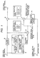
- This noise reduction signal processing circuit is generally used for a display apparatus, for example, a television receiver.
- This noise reduction signal processing circuit is provided with a delaying function 20, an adding function 35, a multiplying function 37, a filtering function 40, a size judging function 50 composed of an adder, and a minimum value detecting function 70.
- the delaying function 20 outputs a delay video signal (A) obtained by adding a delay, which is equivalent to the delay in the output of a median filter 40, to video signals entered from a video signal input terminal T1.
- the adding function 35 outputs noise reduced video signals to the video signal output terminal T2.
- Each of the noise reduced video signals is obtained by adding the delayed video signal (A) outputted from the delaying function 20 and a noise reduction signal.
- the multiplying function 37 generates a noise reduction signal by multiplying the minimum value data ⁇ outputted from the minimum value detecting function 70 by a noise denying polarity signal.
- the filtering circuit 40 is composed of a median filter, as well as a plurality of delaying circuits 41 and 42 and an intermediate value selecting circuit 43 that are all tandem-connected.
- This filtering circuit outputs a voltage level intermediate value selected from among the values of the voltage levels of video signals detected at least at three different times, that is, at a time t, before the time t, and after the time t or outputs the most frequently appearing data of the same value selected from among voltage level values of digital video signals detected at least at those three different times t if no intermediate value is found from those voltage levels.
- the selected intermediate voltage level value or the most-frequently appearing data is outputted as a reference signal (B).
- the size judging function 50 compares the delayed video signal (A) with the reference signal (B), thereby judging which of those signals is larger, and then outputs the noise denying polarity signal that indicates the direction in which an object noise is reduced.
- the function 50 also outputs absolute value data (
- the minimum value detecting function 70 outputs L at
- L, and
- are decided according to the result of comparison between the absolute value data (
- This configuration of the apparatus of the present invention makes it possible to reduce the noise level using a noise reduction signal obtained by restricting each difference signal at a fixed level.
- the difference signal is obtained through a comparison between an inputted video signal and a reference signal obtained via a median filter. Consequently, the above apparatus also makes it possible to reduce various voltage level noises included in video signals without adding a new distortion signal (distortion preventive signal) to those video signals, thereby obtaining video signals from which noises are reduced accurately and significantly.
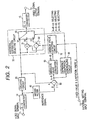
- the noise reduction signal processing apparatus of the present invention comprises an A/D converter 10, a delaying circuit 20, an addition/subtraction selecting circuit 30, a D/A converter 15, a median filter 40, a subtracter 50, an absolute value converting circuit 60, a minimum value detecting circuit 70, and a difference adaptation controlling circuit 80.
- the apparatus further includes a video input terminal T1, a video output terminal T2, and an external input terminal T3.
- the addition/subtraction selecting circuit 30 comprises an adder 31, a subtracter 32, and a selecting circuit 33.
- Video signals entered from the video input terminal T1 include noise.
- the video signals are then sampled with a predetermined sampling clock in the A/D converter 10, then outputted as digital video signals.
- the median filter 40 On receiving each of those video signals, the median filter 40 outputs a voltage level intermediate value selected from among the voltage level values of those video signals detected at least at three different times, that is, at a time t, before the time t, and after the time t, or outputs the most frequently appearing data of the voltage levels having the same value, this being selected from among digital video signals detected at least at those three different times if no intermediate value is found from those video signals.
- the median filter 40 can smooth small amplitude signals in the high range more effectively than low-path filters can.
- the median filter also outputs large amplitude signals appearing at rising and falling portions so as not to lose their precipitous shapes and timings, thereby allowing those signals to be outputted as reference signals.
- Those reference signals can be taken to be as original ideal video signals from which noise elements have already been reduced satisfactorily.
- This selectively outputted video signal (B) is entered to the subtracter 50.
- the video signal entered to the delay circuit 20 is output after it is delayed according to the delay of the video signal in the median filter 40.
- This delayed and outputted video signal (A) is entered to the other input terminal of the subtracter 50.
- the video signal outputted from the delay circuit 20 is entered to the input terminal (a) of the selecting circuit 33 of the addition/subtraction selecting circuit 30, as well as to the input terminals of both adder 31 and subtracter 32 respectively.
- the subtracter 50 outputs difference signal data (A-B) obtained by subtracting the reference signal data (B) outputted from the median filter 40 from the video signal data (A) outputted from the delay circuit 20.
- Most of the components of this difference data are noise components, but the difference data will probably include high range components of video signals as well.
- This difference data also includes positive or negative sign information, since it is a value obtained by subtracting the reference signal from each of noise-included original signals.
- This difference signal data (A-B) is entered to both the absolute value converting circuit 60 and the difference adaptation controlling circuit 80, then converted to an absolute value (
- ) of this difference signal is entered to the minimum value detecting circuit 70.
- a limitation value (L) is also entered to the other input terminal of the minimum value detecting circuit 70 via the external input terminal T3.
- the limitation value (L) is equivalent to the upper limit value of a noise reduction value.
- the minimum value detecting circuit 70 compares the absolute value data (
- the adder 31 outputs the result of addition of the video signal (A) outputted from the delay circuit 20 and the minimum value data ( ⁇ ) outputted from the minimum value detecting circuit 70. The result of this addition is entered to the input terminal (b) of the selecting circuit 33.
- the subtracter 32 outputs the result of subtraction obtained by subtracting the minimum value data ( ⁇ ) outputted from the minimum value detecting circuit 70 from the video signal outputted from the delay circuit 20. The result of this subtraction is entered to the input terminal (c) of the selecting circuit 33.
- Each signal entered to the input terminals (a), (b), and (c) of the selecting circuit 33 is selected and outputted by the difference adaptation controlling circuit 80 using a selecting method to be described later.
- the difference adaptation controlling circuit 80 thus selects and outputs the original signal entered to the input terminal (a) of the selecting circuit 33 as it is. If the value of the difference data is positive, the difference adaptation controlling circuit 80 selects the video signals entered to the input terminal (c) of the selecting circuit 33 and outputs the video signals.
- the difference adaptation controlling circuit 80 subtracts difference data, which is equivalent to a noise value, from the original signal, thereby outputting noise reduced video signals. If the value of difference data is negative, the difference adaptation controlling circuit 80 selects so as to output the video signal entered to the input terminal (b) of the selecting circuit 33 and outputs video signals. More concretely, since the value of negative difference data means that an entered noise-included video signal, which is an original signal, is smaller than the reference signal value, the difference adaptation controlling circuit 80 adds difference data, which is equivalent to a noise value, to the original signal, thereby outputting noise reduced video signals.
- the minimum value detecting circuit 70 uses a limitation value (L) entered from the terminal T3 to limit the absolute value data (
- L limitation value
- the difference data also includes high range components of video signals, although most of difference data consists of noise components. Consequently, if difference data is composed of high range components of an original signal, then a high range component signal, which has a large amplitude level of a video signal, can keep the noise reduction amount at a low level, realized through the arithmetic operation performed by the addition/subtraction selecting circuit 30.
- the noise reduced digital video signals outputted from the selecting circuit 33 in such a way are sampled at a predetermined sampling clock in the D/A converter 15 and are converted to noise-reduced analog video signals and outputted from the video output terminal T2.
- the median filter 40 can generate the reference signal (B), which is an ideal video signal including almost no high range component signal, which is mostly noise components.
- the subtracter 50 compares this generated reference signal (B) with the noise-included input video signal(A), thereby extracting a difference data signal from actual video signals.
- the difference data signal is a high range component signal, most of which consists of noise components.
- the subtracter 50 judges the difference in size between both signals, the subtracter 50 can also control the selection of an arithmetic operation method of the addition/subtraction selecting circuit 30.
- the absolute value converting circuit 60 finds the absolute value of this difference data.
- the minimum value detecting circuit 70 limits the difference data converted to an absolute value to the voltage level of the difference data using a limitation value (L) which is set externally.
- this example makes it possible to include noise components in the difference data obtained from the minimum value detecting circuit 70 by removing high range information components from actual inputted video signals as much as possible, as well as to limit the noise reduction level freely as needed with a fixed value set externally as required.
- the addition/subtraction selecting circuit 30 can remove noise components included in input video signals using the difference data generated from actual video signals in such a way.
- the level of a noise can be reduced using a noise reduction signal obtained by limiting to a fixed level a signal (difference signal) obtained through a comparison between an input video signal and a reference signal entered through a median filter. Therefore, this embodiment makes it possible to reduce various voltage level noises included in video signals without adding a new distortion signal (distortion preventive signal) to those signals, thereby obtaining accurately and satisfactorily noise-reduced video signals.
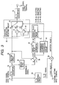
- Fig. 3 is a block diagram of another embodiment of the noise reduction signal processing apparatus of the present invention.
- the same reference numerals are used for the same functions as those shown in Fig. 2. but differs from the example illustrated in Fig. 2 by the provision of an S/N detecting circuit 90 and an adder 55.
- the S/N detecting circuit 90 detects video signal noise components from the synchronizing signal, etc. in which no image signal is included in the vertical blanking period of input video signals, thereby detecting the S/N level.
- the S/N detecting circuit 90 outputs a zero S/N level signal when a predetermined S/N level is detected, a minus S/N level signal when the object S/N level is larger than this zero S/N level, and a plus S/N level signal when the object S/N level is smaller than the zero S/N level. Furthermore, the S/N level signal outputted from the S/N detecting circuit 90 is assumed to be a value divided into some steps corresponding to those S/N levels. This value divided into some steps is entered to the adder 55. The other input terminal of the adder 55 receives a fixed value (S), which is equivalent to the upper limit value of a noise reduction value via the external input terminal T3 shown in the example shown in Fig. 3.
- S fixed value
- the adder 55 outputs a limitation value (L), which is smaller than the fixed value (S) set via the external input terminal T3 when the object S/N level is high, that is, when the S/N level is satisfactory, and then outputs a limitation value (L), which is larger than the fixed value (S) set via the external input terminal T3 when the object S/N level is low, that is, when the S/N level is not satisfactory.
- This limitation signal (L) is entered to the minimum value detecting circuit 70.
- the noise reduction signal processing apparatus of the present invention can also be used for a television unit. In this case, the effect of the apparatus will appear more significantly.
- the noise reduction processing circuit that uses a median filter is also very effective for noise-contained video signals, so that the circuit makes it possible to obtain video signals from which noises are removed accurately and satisfactorily without adding a new distortion preventive signal to those video signals.
Landscapes
- Engineering & Computer Science (AREA)
- Multimedia (AREA)
- Signal Processing (AREA)
- Picture Signal Circuits (AREA)
- Image Processing (AREA)
Applications Claiming Priority (2)
| Application Number | Priority Date | Filing Date | Title |
|---|---|---|---|
| JP18712798 | 1998-07-02 | ||
| JP18712798A JP3863294B2 (ja) | 1998-07-02 | 1998-07-02 | ノイズ低減信号処理回路および映像表示装置 |
Publications (2)
| Publication Number | Publication Date |
|---|---|
| EP0969658A1 EP0969658A1 (en) | 2000-01-05 |
| EP0969658B1 true EP0969658B1 (en) | 2006-09-06 |
Family
ID=16200599
Family Applications (1)
| Application Number | Title | Priority Date | Filing Date |
|---|---|---|---|
| EP99305196A Expired - Lifetime EP0969658B1 (en) | 1998-07-02 | 1999-07-01 | Noise reduction signal processing circuit and display apparatus |
Country Status (4)
| Country | Link |
|---|---|
| US (1) | US6195132B1 (enExample) |
| EP (1) | EP0969658B1 (enExample) |
| JP (1) | JP3863294B2 (enExample) |
| DE (1) | DE69933090T2 (enExample) |
Families Citing this family (25)
| Publication number | Priority date | Publication date | Assignee | Title |
|---|---|---|---|---|
| JP2001045336A (ja) * | 1999-07-29 | 2001-02-16 | Matsushita Electric Ind Co Ltd | ノイズ検出装置、ノイズ検出方法、信号処理装置および信号処理方法 |
| GB2361133B (en) | 2000-04-07 | 2004-04-14 | Snell & Wilcox Ltd | Video signal processing |
| DE10146582A1 (de) * | 2001-09-21 | 2003-04-24 | Micronas Munich Gmbh | Vorrichtung und Verfahren zur Teilbandzerlegung von Bildsignalen |
| KR100396557B1 (ko) * | 2001-10-11 | 2003-09-02 | 삼성전자주식회사 | 영상 신호의 노이즈 감쇄 방법 및 그 장치 |
| KR100429804B1 (ko) * | 2001-12-29 | 2004-05-03 | 삼성전자주식회사 | 적응적 영상 노이즈 감쇄 장치 및 그 방법 |
| US7092584B2 (en) | 2002-01-04 | 2006-08-15 | Time Warner Entertainment Company Lp | Registration of separations |
| US6947607B2 (en) | 2002-01-04 | 2005-09-20 | Warner Bros. Entertainment Inc. | Reduction of differential resolution of separations |
| JP4550502B2 (ja) * | 2003-07-16 | 2010-09-22 | 三星電子株式会社 | 並列構造のntsc除去フィルタ及びフィルタリング方法 |
| US7274828B2 (en) * | 2003-09-11 | 2007-09-25 | Samsung Electronics Co., Ltd. | Method and apparatus for detecting and processing noisy edges in image detail enhancement |
| US7570831B2 (en) * | 2004-04-29 | 2009-08-04 | Hewlett-Packard Development Company, L.P. | System and method for estimating image noise |
| JP4551873B2 (ja) * | 2006-02-07 | 2010-09-29 | Okiセミコンダクタ株式会社 | 雑音量測定装置 |
| JP4470901B2 (ja) * | 2006-03-31 | 2010-06-02 | ソニー株式会社 | 撮像装置、高周波成分検出回路、高周波成分検出方法及びコンピュータプログラム |
| JP4863767B2 (ja) * | 2006-05-22 | 2012-01-25 | ソニー株式会社 | 映像信号処理装置及び画像表示装置 |
| TWI343206B (en) * | 2006-10-12 | 2011-06-01 | Novatek Microelectronics Corp | Noise estimator device of a video decoder and related method |
| JP2009212587A (ja) * | 2008-02-29 | 2009-09-17 | Toshiba Corp | フィルタ回路、これを用いた受信機及びフィルタリング方法 |
| TWI387335B (zh) * | 2008-05-26 | 2013-02-21 | Novatek Microelectronics Corp | 信號調節電路及其視訊裝置 |
| US8687124B2 (en) | 2010-02-15 | 2014-04-01 | Sharp Kabushiki Kaisha | Signal processing device, integrated circuit, control program, and computer readable recording medium |
| WO2011102046A1 (ja) * | 2010-02-18 | 2011-08-25 | シャープ株式会社 | 画像処理システム及び表示装置 |
| US8687125B2 (en) | 2010-05-18 | 2014-04-01 | Sharp Kabushiki Kaisha | Image processing system and display device for carrying out subtraction or addition of a pixel value of a target pixel in accordance with a value equivalent to a noise quantity |
| WO2012060290A1 (ja) * | 2010-11-02 | 2012-05-10 | シャープ株式会社 | 画像処理装置、画像処理方法及び表示装置 |
| JP2014150296A (ja) * | 2011-05-25 | 2014-08-21 | Sharp Corp | 画像処理装置及び画像処理方法 |
| JP6059451B2 (ja) * | 2011-06-23 | 2017-01-11 | ローム株式会社 | 発光体駆動装置及びこれを用いた照明機器 |
| JP6064462B2 (ja) * | 2012-09-07 | 2017-01-25 | シャープ株式会社 | ノイズ低減装置、プロセッサ、映像表示装置、ノイズ低減方法およびプログラム |
| US9241128B2 (en) | 2013-02-14 | 2016-01-19 | Warner Bros. Entertainment Inc. | Video conversion technology |
| WO2017120234A1 (en) * | 2016-01-05 | 2017-07-13 | The Trustees Of Dartmouth College | Fast amplitude detector and automatic gain control |
Family Cites Families (12)
| Publication number | Priority date | Publication date | Assignee | Title |
|---|---|---|---|---|
| US4562470A (en) * | 1983-04-07 | 1985-12-31 | Centre De Recherche Industrielle Du Quebec | Electrical noise reducer for T.V. signals |
| JP2508442B2 (ja) * | 1987-06-09 | 1996-06-19 | ソニー株式会社 | ノイズ除去回路 |
| US5257109A (en) * | 1990-07-02 | 1993-10-26 | Akai Electric Co., Ltd. | Magnetic recording and reproducing apparatus |
| DE4137404C2 (de) * | 1991-11-14 | 1997-07-10 | Philips Broadcast Television S | Verfahren zur Reduktion von Rauschen |
| JP3006290B2 (ja) * | 1992-06-25 | 2000-02-07 | 松下電器産業株式会社 | ノイズ低減装置 |
| US6097847A (en) * | 1993-05-31 | 2000-08-01 | Nec Corporation | Method of and apparatus for calculating sharpness of image and apparatus for sharpening image |
| DE4319342C2 (de) * | 1993-06-11 | 1999-05-20 | Philips Patentverwaltung | Verfahren zur Reduktion von Störungen |
| TW297202B (enExample) * | 1993-10-13 | 1997-02-01 | Rca Thomson Licensing Corp | |
| EP0660595B1 (en) * | 1993-12-20 | 2000-03-15 | Matsushita Electric Industrial Co., Ltd. | A noise reducer |
| US5574512A (en) * | 1994-08-15 | 1996-11-12 | Thomson Consumer Electronics, Inc. | Motion adaptive video noise reduction system |
| KR0160690B1 (ko) * | 1995-04-29 | 1999-01-15 | 김광호 | 영상신호 부호화/복호화장치에 있어서 블럭킹 효과 제거회로 |
| GB2305054B (en) * | 1995-08-29 | 2000-03-22 | British Broadcasting Corp | Blemish concealment in video signals |
-
1998
- 1998-07-02 JP JP18712798A patent/JP3863294B2/ja not_active Expired - Fee Related
-
1999
- 1999-07-01 DE DE69933090T patent/DE69933090T2/de not_active Expired - Fee Related
- 1999-07-01 US US09/345,489 patent/US6195132B1/en not_active Expired - Fee Related
- 1999-07-01 EP EP99305196A patent/EP0969658B1/en not_active Expired - Lifetime
Also Published As
| Publication number | Publication date |
|---|---|
| JP2000022992A (ja) | 2000-01-21 |
| JP3863294B2 (ja) | 2006-12-27 |
| DE69933090T2 (de) | 2007-04-05 |
| DE69933090D1 (de) | 2006-10-19 |
| US6195132B1 (en) | 2001-02-27 |
| EP0969658A1 (en) | 2000-01-05 |
Similar Documents
| Publication | Publication Date | Title |
|---|---|---|
| EP0969658B1 (en) | Noise reduction signal processing circuit and display apparatus | |
| KR930002906B1 (ko) | 윤곽 보정회로 | |
| US7738042B2 (en) | Noise reduction device for a video signal and noise reduction method for a video signal | |
| EP0396746B1 (en) | Picture receiver controller | |
| EP0040801B1 (en) | Automatic equalizer | |
| US6133942A (en) | Co-channel interference canceler and driving method therefor | |
| JPH0730785A (ja) | 雑音低減方法及びそのための回路 | |
| EP0720391A2 (en) | Digital processing apparatus | |
| US5612752A (en) | Noise reduction method and apparatus | |
| KR900000128B1 (ko) | 빗살형 필터 | |
| JPS62272673A (ja) | ノイズリデユ−サ | |
| KR100346079B1 (ko) | 비디오신호용히스토그램연산장치 | |
| US5214510A (en) | Adaptive digital aperture compensation and noise cancel circuit | |
| JP2601344B2 (ja) | 雑音低減兼垂直輪郭補償回路 | |
| JP3781590B2 (ja) | ノイズ低減信号処理装置 | |
| JPS6346881A (ja) | デジタル輪郭補正回路 | |
| JP2576517B2 (ja) | ノイズ低減回路 | |
| JP2756697B2 (ja) | ビデオ信号処理装置 | |
| JP3130429B2 (ja) | 動き検出回路 | |
| JP2517200B2 (ja) | ディジタル映像信号のノイズ除去装置 | |
| JP2506205B2 (ja) | 黒レベル補正装置 | |
| KR100218445B1 (ko) | 적응형 잡음 감소기 | |
| JP3354065B2 (ja) | 動き検出回路 | |
| KR940002416B1 (ko) | 동기신호삽입방식 및 회로 | |
| JP2768550B2 (ja) | 雑音除去装置 |
Legal Events
| Date | Code | Title | Description |
|---|---|---|---|
| PUAI | Public reference made under article 153(3) epc to a published international application that has entered the european phase |
Free format text: ORIGINAL CODE: 0009012 |
|
| 17P | Request for examination filed |
Effective date: 19990721 |
|
| AK | Designated contracting states |
Kind code of ref document: A1 Designated state(s): AT BE CH CY DE DK ES FI FR GB GR IE IT LI LU MC NL PT SE |
|
| AX | Request for extension of the european patent |
Free format text: AL;LT;LV;MK;RO;SI |
|
| AKX | Designation fees paid |
Free format text: DE FR GB |
|
| GRAP | Despatch of communication of intention to grant a patent |
Free format text: ORIGINAL CODE: EPIDOSNIGR1 |
|
| RIN1 | Information on inventor provided before grant (corrected) |
Inventor name: SUDO, KOICHI Inventor name: TSURU, YASUTAKA Inventor name: SUGIYAMA, MASATO Inventor name: NAGATA, TATSUO Inventor name: TAKATA, HARUKI Inventor name: MATONO, TAKAAKI Inventor name: KIMURA, KATSUNOBU |
|
| GRAS | Grant fee paid |
Free format text: ORIGINAL CODE: EPIDOSNIGR3 |
|
| GRAA | (expected) grant |
Free format text: ORIGINAL CODE: 0009210 |
|
| AK | Designated contracting states |
Kind code of ref document: B1 Designated state(s): DE FR GB |
|
| REG | Reference to a national code |
Ref country code: GB Ref legal event code: FG4D |
|
| RIN1 | Information on inventor provided before grant (corrected) |
Inventor name: SUDO, KOICHI Inventor name: TSURU, YASUTAKA Inventor name: SUGIYAMA, MASATO Inventor name: NAGATA, TATSUO Inventor name: TAKATA, HARUKI Inventor name: MATONO, TAKAAKI Inventor name: KIMURA, KATSUNOBU |
|
| REF | Corresponds to: |
Ref document number: 69933090 Country of ref document: DE Date of ref document: 20061019 Kind code of ref document: P |
|
| ET | Fr: translation filed | ||
| PLBE | No opposition filed within time limit |
Free format text: ORIGINAL CODE: 0009261 |
|
| STAA | Information on the status of an ep patent application or granted ep patent |
Free format text: STATUS: NO OPPOSITION FILED WITHIN TIME LIMIT |
|
| 26N | No opposition filed |
Effective date: 20070607 |
|
| PGFP | Annual fee paid to national office [announced via postgrant information from national office to epo] |
Ref country code: GB Payment date: 20070720 Year of fee payment: 9 |
|
| PGFP | Annual fee paid to national office [announced via postgrant information from national office to epo] |
Ref country code: DE Payment date: 20070924 Year of fee payment: 9 |
|
| PGFP | Annual fee paid to national office [announced via postgrant information from national office to epo] |
Ref country code: FR Payment date: 20070516 Year of fee payment: 9 |
|
| GBPC | Gb: european patent ceased through non-payment of renewal fee |
Effective date: 20080701 |
|
| PG25 | Lapsed in a contracting state [announced via postgrant information from national office to epo] |
Ref country code: DE Free format text: LAPSE BECAUSE OF NON-PAYMENT OF DUE FEES Effective date: 20090203 |
|
| REG | Reference to a national code |
Ref country code: FR Ref legal event code: ST Effective date: 20090331 |
|
| PG25 | Lapsed in a contracting state [announced via postgrant information from national office to epo] |
Ref country code: GB Free format text: LAPSE BECAUSE OF NON-PAYMENT OF DUE FEES Effective date: 20080701 |
|
| PG25 | Lapsed in a contracting state [announced via postgrant information from national office to epo] |
Ref country code: FR Free format text: LAPSE BECAUSE OF NON-PAYMENT OF DUE FEES Effective date: 20080731 |