EP0959615B1 - Farbbildverarbeitungsgerät - Google Patents
Farbbildverarbeitungsgerät Download PDFInfo
- Publication number
- EP0959615B1 EP0959615B1 EP99202644A EP99202644A EP0959615B1 EP 0959615 B1 EP0959615 B1 EP 0959615B1 EP 99202644 A EP99202644 A EP 99202644A EP 99202644 A EP99202644 A EP 99202644A EP 0959615 B1 EP0959615 B1 EP 0959615B1
- Authority
- EP
- European Patent Office
- Prior art keywords
- color
- image
- pattern
- signal
- color component
- Prior art date
- Legal status (The legal status is an assumption and is not a legal conclusion. Google has not performed a legal analysis and makes no representation as to the accuracy of the status listed.)
- Expired - Lifetime
Links
- 238000012545 processing Methods 0.000 title claims description 5
- 238000000034 method Methods 0.000 claims description 29
- 230000010363 phase shift Effects 0.000 claims 1
- 238000012546 transfer Methods 0.000 description 63
- 239000003086 colorant Substances 0.000 description 59
- 230000001788 irregular Effects 0.000 description 33
- 230000008859 change Effects 0.000 description 20
- 230000006866 deterioration Effects 0.000 description 17
- 230000003111 delayed effect Effects 0.000 description 15
- 230000004044 response Effects 0.000 description 10
- 230000015572 biosynthetic process Effects 0.000 description 9
- 238000010586 diagram Methods 0.000 description 9
- 239000011159 matrix material Substances 0.000 description 7
- 238000007639 printing Methods 0.000 description 6
- 238000009826 distribution Methods 0.000 description 5
- 230000004048 modification Effects 0.000 description 5
- 238000012986 modification Methods 0.000 description 5
- 230000003287 optical effect Effects 0.000 description 5
- 230000001934 delay Effects 0.000 description 4
- 230000000694 effects Effects 0.000 description 4
- 238000005516 engineering process Methods 0.000 description 4
- 230000008569 process Effects 0.000 description 4
- 230000003068 static effect Effects 0.000 description 4
- 238000004140 cleaning Methods 0.000 description 3
- 239000004065 semiconductor Substances 0.000 description 3
- 230000000007 visual effect Effects 0.000 description 3
- 239000003795 chemical substances by application Substances 0.000 description 2
- 230000001747 exhibiting effect Effects 0.000 description 2
- 238000003672 processing method Methods 0.000 description 2
- 238000000926 separation method Methods 0.000 description 2
- 230000009471 action Effects 0.000 description 1
- 238000006243 chemical reaction Methods 0.000 description 1
- 210000000078 claw Anatomy 0.000 description 1
- 238000010276 construction Methods 0.000 description 1
- 238000011161 development Methods 0.000 description 1
- 238000005286 illumination Methods 0.000 description 1
- 238000003384 imaging method Methods 0.000 description 1
- 230000006872 improvement Effects 0.000 description 1
- 230000009467 reduction Effects 0.000 description 1
Images


Classifications
-
- H—ELECTRICITY
- H04—ELECTRIC COMMUNICATION TECHNIQUE
- H04N—PICTORIAL COMMUNICATION, e.g. TELEVISION
- H04N1/00—Scanning, transmission or reproduction of documents or the like, e.g. facsimile transmission; Details thereof
- H04N1/46—Colour picture communication systems
- H04N1/52—Circuits or arrangements for halftone screening
Definitions
- the present invention relates to a color image processing apparatus, and, more particularly, to a color image processing apparatus for use in a printer of an electronic photography system or a thermal transfer system.
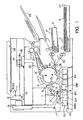
- Fig. 1 illustrates a conventional copying machine of a full color electronic photography system and serving as a multicolor image forming apparatus.
- a photosensitive drum 1 having, on the surface thereof, a photosensitive layer for the electronic photography is rotated in a direction designated by an arrow X.
- a primary charger 2 is disposed to the left of the photosensitive drum 1.
- a surface potential meter 3 for measuring the surface potential of the photosensitive drum 1 is positioned off to the lower left of the photosensitive drum 1.
- a developing device 50 on which a plurality of developing units 51M, 51C, 51Y and 51Bk, which respectively use a two-component developer prepared by mixing toner and a carrier, are loaded is disposed below the photosensitive drum 1, the developing device 50 being capable of moving laterally.
- a transfer device 5 is positioned off to the upper right to the photosensitive drum 1.
- a pre-electrostatic charge remover 6 is disposed substantially above the photosensitive drum 1, the pre-electrostatic charge remover 6 acting to reduce the adhesion force between the toner left on the surface of the photosensitive drum 1 and the photosensitive drum 1 after the transfer operation has been performed so that the surface of the photosensitive drum 1 is easily cleaned.
- a cleaning device 7 is positioned off to the upper left to the photosensitive drum 1.
- an optical system 10 is disposed in the upper portion of the copying machine so that the image of an original document placed on a platen 28 is projected on to the photosensitive drum 1 by an exposing portion 9 disposed between the primary charger 2 and the surface potential meter 3.
- the optical system 10 comprises a first scanning mirror 11 and second and third scanning mirrors 12 and 13 moving in the same direction as the direction in which the first scanning mirror 11 moves, the second and third scanning mirrors 12 and 13 moving at half speed of that of the first scanning mirror 11.
- the optical system 10 further comprises an imaging lens 14, a CCD 15 integrally formed with the B, G and R filters, a laser scanner unit 16 and stationary mirrors 17 and 18.
- An original document illumination light source 20 of the optical system 10 is arranged to move together with the first scanning mirror 11. Therefore, the reflected light image of the original document scanned by the first to the third scanning mirrors 11 to 13 passes through the lens 14 before the color of it is separated by the CCD 15 having a BGR four-color separating filter so that it is converted into an electric signal. Then, a signal denoting information about the original document thus obtained is subjected to an information process such as the A/D conversion before it is, as a video signal, supplied to a microprocessor unit (to be called an "MPU" hereinafter), which controls the overall function of the copying machine.
- the MPU causes a laser unit to oscillate a laser beam via a laser driver, the laser beam being then applied/not applied to the photosensitive drum 1. As a result, the copying sequence is started.
- a fixing device 20 and a paper feeding device 30 are disposed in the right portion of the copying machine.
- a copying-paper conveyance systems 25 and 35 are respectively disposed between the transfer drum 5 and the fixing devices 20 and between the same and the paper feeding device 30.
- the photosensitive drum 1 is, for each color separated by the CCD 15, subjected to charging, exposing, developing, transferring and cleaning processes by the primary charger 2, the optical system 10, the developing device 50, the transfer device 5 and the cleaning device 7.
- the developing device 50 comprises developing units 51M (a Magenta developing unit), 51C (a Cyan developing unit), 51Y (a Yellow developing unit) and 51Bk (a Black developing unit) so as to cause the developing units to make the latent image for each color, which has been separated, to be a visual image.
- 51M a Magenta developing unit
- 51C a Cyan developing unit
- 51Y a Yellow developing unit
- 51Bk a Black developing unit
- the transfer device 5 usually comprises a transfer drum 5b having a gripper 5a for gripping, on the outer surface thereof, a transfer agent, that is, transfer paper P.
- the transfer device 5 grips, by its gripper 5a, the front portion of the transfer paper P supplied from a transfer paper cassette 31 or 32 of the paper feeder 30 via a transfer paper conveyance system 35. Then, the transfer paper P is attracted to the transfer drum 5b by an action of an attraction charger 4 disposed in the transfer drum 5b. Then, the transfer device 5 rotates and conveys the transfer paper P so as to cause the visual image for each color on the photosensitive drum 1 to be transferred to the transfer paper P. In the transfer zone, a transfer charger 5c is disposed in the transfer drum 5.
- the transfer paper P to which the visual images for each color, that is, the toner images have been successively transferred, is separated from the gripper 5a before it is separated from the transfer drum 5b by a separating charger 8 and a separating claw 8'. Then, the transfer paper P is sent to the fixing deice 20 by the transfer paper conveyance system 25. The toner image on the transfer paper P is fixed by the fixing device 20 at that position before the transfer paper is discharged to a tray 23.
- the diameter of the transfer drum 5b cannot be enlarged since the size of the copying machine must be reduced. Furthermore, the transfer paper conveyance system 35 and the transfer paper conveyance system 25 positioned to act after the transfer and the separation process are not disposed sufficiently farther from each other in the direction of the rotation of the transfer drum 5b. That is, the position at which the transfer paper P is attracted and the position at which the same is separated are not positioned sufficiently farther from each other with respect to the position at which the image is transferred in the direction of rotation of the transfer drum 5b. Therefore, the following problems arose:
- the photosensitive drum 1 is vibrated when the transfer sheet forming the side surface of the transfer drum 5b is pressed by the transfer paper P.
- the latent image of the first color will deviate with respect to the latent images of other colors.
- a multicolor image forming apparatus is usually structured in such a manner that an image is formed for each color component and they are multiplied so that a multicolor image is formed.
- the image deteriorations are classified into deteriorations for a long period and that for a short period.
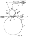
- Fig. 4 is a structural view which schematically illustrates an image forming portion of a color laser printer of the type described above.
- a photosensitive body 101 is being rotated in a direction designated by an arrow A.
- the photosensitive body 101 is equally charged by a charger 103. Then, an image exposure process is performed by an image scanning exposure method in which the image portion is exposed to light by a semiconductor laser which has been modulated in accordance with image data 112 for each color and emitted from a signal generating means 111 and the non-image portion is not exposed. As a result, a static latent image is formed.
- a latent image for the first color is developed by a developing device 105 for the first color so that a toner image is formed on the photosensitive body 101.
- the thus formed image is transferred to transfer paper 107 to be previously supplied to a transfer drum 113.
- the residual toner left on the photosensitive body 101 is cleaned by a cleaner 110.
- the above-described operation is performed for each of the colors so that a multicolor image is formed on the transfer drum 113. Then, the static charge of the transfer paper 107 is separated by a separating charger 108 before the multicolor image is fixed by a fixing device 109. Then, the transfer paper 107 is discharged as designed.
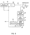
- Fig. 5 is a block diagram which illustrates the structure of a circuit capable of realizing the above-described method.
- Digital data 121 transmitted from a digital data output device 131 is converted into an analog image signal 122 by a D/A converter 132.
- a pattern signal 126 (for example, a triangular wave) is generated by a pattern signal generator 135.
- the pattern signal 126 is arranged in such a manner that its synchronizing signal is a screen clock 125 obtained by dividing (count down to a half period here) a transfer image clock 123 for image data by a reference clock signal 124 generated by an oscillator 133, the dividing operation of the transfer image clock 123 being performed in a timing signal generating circuit 134.
- the analog image signal 122 and the pattern signal 126 are subjected to a comparison by a comparator 136. Then, binary image data 127 is processed in such a manner that data "0" is processed if it has been determined that the analog image signal is larger than the pattern signal 126 and data "1" is processed if it has been determined that the same is smaller than the pattern signal 126.
- the digital image signal is converted into the analog signal before it is subjected to a comparison with a triangular wave of a predetermined period.
- substantially successive pulse width modulation is performed so that a high quality image output exhibiting an excellent gradation can be obtained.
- the circuit in which the above-described pulse width modulation is performed is arranged to comprise a shift register 137 between the timing signal generating circuit 134 and the pattern signal generator 135 so that the phase of the pattern signal 126 is delayed for each of the scanning lines.
- a shift register 137 between the timing signal generating circuit 134 and the pattern signal generator 135 so that the phase of the pattern signal 126 is delayed for each of the scanning lines.
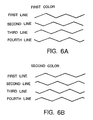
- Figs. 6A and 6B illustrate the waveform of examples of delaying the pattern signal for each of the scanning lines performed by the delay circuit.
- Figs. 7A and 7B are schematic views which illustrate the patterns of the output image of each color, the patterns being realized in response to the pattern signal.
- the recording density was arranged to be 80 dpi (5 pixels correspond to 1 dot) in the main scanning direction and 400 dpi (1 pixel corresponds to 1 dot) in the sub-scanning direction.
- the quantity of the delay of the pattern signal was arranged to be 2/5 dot for the first color and 3/5 dot for the second color.
- the image formation angle was arranged to be 26.6° and -26.6°, respectively.
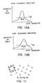
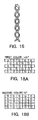
- the reason for this lies in that, when the scanning beam is applied to the position deviated from the desired position, the positions of the dots, which are disposed at substantially the same intervals as those of the surrounding pixels, are deviated as shown in Fig. 11 since the scanning beams for forming the dots display the light quantity distributions as shown in Figs. 10A and 10B. As a result, irregular interference takes place between dots as shown in Fig. 12. Therefore, the problem of this type becomes more critical in proportion to the improvement in the resolution.
- a color image forming apparatus which is capable of modulating the pulse width of each of color component signals by making a comparison with a pattern signal such as a triangular signal for each of the color component signals which constitute the color image signal.
- an apparatus of the type described above employs a method of removing color moire (the deteriorations for a long period) by the pulse width modulation performed in such a manner that a reference signal of a different phase and an image signal are subjected to a comparison for each of colors.
- Japanese Patent Laid-Open No. 62-183670, Japanese Patent Laid-Open No. 62-183676 and Japanese Patent Laid-Open No. 62-183680 have disclosed methods of removing the moire by varying the quantity of delaying the reference signal for each of the lines.
- the deteriorations for a short period can not be removed, and what is worse, the deteriorations for a long period can not be entirely removed.
- the above-described problems are not limited to the color laser beam printer and are common to all of the multicolor image forming apparatus such as an ink jet printer and a thermal transfer printer if it modulates and transmits a multicolor image input signal. Also a dichroic printer of a Black and red colors type or a multicolor printer exceeding two colors encounter the similar problems.
- Figs. 14A to 14D illustrates image forming patterns for the corresponding colors formed by a full color copying agent according to a first example.
- a desired full color image is formed by overlapping images of the corresponding colors by using toner for four colors in order to form a four color full color image.
- the screen angle of 45° in the image forming pattern for Magenta (M) which is the first color and the screen angle of 26.6° for Black (Bk) which is the final color are respectively arrange to be different from the screen angle of 0° for Cyan (C) which is the second color and that for Yellow (Y) which is the third color.
- Fig. 15 is a block diagram which illustrates the structure of an image forming pattern generating device for use in a first embodiment of the present invention.
- a multicolor image signal A (four types of digital signals for M, C, Y and Bk according to this example) is converted into an analog signal a by a D/A converter 201 for each color component.
- a reference signal b (according to this example, it is a triangular wave) determined for each color component is processed under a control of a CPU 203 by utilizing a clock divided from a high speed clock by a pulse pattern generator 202.
- the reference signal b is supplied to a delay line 206 so that it is delayed.
- eight types of delay patterns are provided and a selector 207 selects any one of the eight types. As shown in Figs.
- the eight delay patterns are prepared which is arranged in such a manner that a delay of a quarter of one pixel is one unit of the quantity of delay.
- one unit of the reference unit of the pulse width modulation (PWM) is arranged to be two pixels.
- the eight types of the delay patterns are the patterns in response to PWM signals (omitted from illustration) each of which is delayed by 0/4 to 7/4 pixel.
- Each of the signals denoting Y, M, C and Bk is arranged to correspond to any one of the above-described 8 types of delay patterns.
- the selector 207 selects any one of the delay patterns for lines of Y, M, C and Bk.
- the selector 207 reads delay pattern information for each line by using a phase change quantity pattern generator 204.
- the pattern generator 204 comprises a RAM which stores delay pattern information to be selected for each line for each color.
- a counter 205 counts a horizontal synchronizing signal in such a manner that counting from 1 to 8 is repeated for each line.
- the selector 207 successively selects the delay pattern in accordance with the delay pattern written in the pattern generator 204 whenever the counter 205 performs the counting operation so as to output it,as a reference signal C.
- the unit of the triangular wave is arranged in such a manner that one unit (dot) is composed of two pixels (that is, the period of the triangular wave corresponds to the two pixels).
- the quantity of the delay is arranged in such a manner that one unit is composed of a quarter pixel.
- the analog signal a is subjected to a comparison with the reference signal c by a comparator 208 so that it is made to be a PWM signal d before it is amplified by an amplifier 209. As a result, a processed signal B thus formed is transmitted.
- the above-described operation is performed for each of the color components so that the component M is not delayed for the odd number lines but is delayed by 4/4 pixel for the even number lines so that the image is formed at a screen angle of 45° (see Fig. 14A).
- the components C and Y are not delayed for all of the lines, that is, image forming is performed at a screen angle of 0° (see Figs. 14B and 14C).
- outputs corresponding to all of the colors are obtained in the full color copying machine as a multiplied image.
- the screen angle at the image forming for the first and the fourth colors and that for the second and the third colors are different from each other. As a result, irregular color can be prevented as shown in Fig. 16.
- the present invention is not limited to a full color image formed by four colors but is preferably employed in any of the structures which outputs a multicolor image formed by two colors or more.
- Figs. 17A to 17C illustrate examples of image forming patters according to a first embodiment at the time of forming the full colour image formed by three colours M, C and Y.
- Figs. 18 and 19 illustrate examples of image forming patterns of dichroic multiplied image formed by, for example, M + C (B), C + Y (G) or Y + M (R).
- the present invention is not limited according to the above-described first embodiment. It can be preferably employed in any of apparatus capable of forming a multi-image formed by two or more colors such as a thermal transfer printer, an LED (Light Emitting Diode) printer and an ink jet printer.
- the screen angle of the color the image of which is formed first or last is arranged to be different from that of other colors. Therefore, color deviations and irregular color in the first and the final color and color tone change at each printing can be prevented in the multicolor image forming apparatus. As a result, the image quality can always be stabilized.
- Fig. 4 is a structural view which schematically illustrates an image forming portion of a conventional colour laser printer.
- a photosensitive body 101 is being rotated in a direction designated by an arrow A.
- the photosensitive body 101 is equally charged by a charger 103. Then, an image exposure process is performed by an image scanning exposure method in which the image portion is exposed to light by a semiconductor laser which has been modulated in accordance with image data 112 for each color and emitted from a signal generating means 111 and the non-image portion is not exposed. As a result, a static latent image is formed.
- a latent image for the first color is developed by a developing device 105 for the first color so that a toner image is formed on the photosensitive body 101.
- the thus formed image is transferred to transfer paper 107 to be previously supplied to a transfer drum 113.
- the residual toner left on the photosensitive body 101 is cleaned by a cleaner 110.
- the above-described operation is performed for each of the colors so that a multicolor image is formed on the transfer drum 113. Then, the static charge of the transfer paper 107 is separated by a separating charger 108 before the multicolor image is fixed by a fixing device 109. Then, the transfer paper 107 is discharged as designed.
- Fig. 5 is a block diagram which illustrates the structure of a circuit capable of realizing the above-described method.
- Digital data 121 transmitted from a digital data output device 131 is converted into an analog image signal 122 by a D/A converter 132.
- a pattern signal 126 (for example, a triangular wave) is generated by a pattern signal generator 135.
- the pattern signal 126 is arranged in such a manner that its synchronizing signal is a screen clock 125 obtained by dividing (count down to a half period here) a transfer image clock 123 for image data by a reference clock signal 124 generated by an oscillator 133, the dividing operation of the transfer image clock 123 being performed in a timing signal generating circuit 134.
- the analog image signal 122 and the pattern signal 126 are subjected to a comparison by a comparator 136. Then, binary image data 127 is processed in such a manner that data "0" is processed if it has been determined that the analog image signal is larger than the pattern signal 126 and data "1" is processed if it has been determined that the same is smaller than the pattern signal 126.
- the digital image signal is converted into the analog signal before it is subjected to a comparison with a triangular wave of a predetermined period.
- substantially successive pulse width modulation is performed so that a high quality image output exhibiting an excellent gradation can be obtained.
- the circuit in which the above-described pulse width modulation is performed is arranged to comprise a shift register 137 between the timing signal generating circuit 134 and the pattern signal generator 135 so that the phase of the pattern signal 126 is delayed for each of the scanning lines.
- a shift register 137 between the timing signal generating circuit 134 and the pattern signal generator 135 so that the phase of the pattern signal 126 is delayed for each of the scanning lines.
- Figs. 6A and 6B illustrate the waveform of examples of delaying the pattern signal for each of the scanning lines performed by the delay circuit.
- Figs. 7A and 7B are schematic views which illustrate the patterns of the output image of each color, the patterns being realized in response to the pattern signal.
- the recording density was arranged to be 80 dpi (5 pixels correspond to 1 dot) in the main scanning direction and 400 dpi (1 pixel corresponds to 1 dot) in the sub-scanning direction.
- the quantity of the delay of the pattern signal was arranged to be 2/5 dot for the first color and 3/5 dot for the second color.
- the image formation angle was arranged to be 26.6° and -26.6°, respectively.
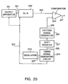
- Fig. 20 is a block diagram which illustrates a pulse width modulation circuit for a color laser printer.
- the basic structure according to this circuit is arranged to be the same as that according to the conventional structure shown in Fig. 5.
- the resolution realized by a pattern signal generator 335 and the quantity of delay realized by a shift register 337 are properly determined so that substantially-elongated pixels having different image forming angles for each of the color components are formed.
- the other elements except for the pattern signal generator 335 and the shift register 337, that is, the output device 331, the D/A converter 332, the comparator 336, the oscillator 333 and the timing signal generating circuit 334 are the same as those of the structure shown in Fig. 5. Therefore, their descriptions are omitted here.
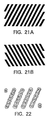
- Figs. 21A and 21B are schematic views which illustrate a case in which the substantially elongated pixels are transmitted by the colors described above (referring to the drawing, two colors are employed).
- slant and thick lines illustrate a status in which the image pattern is formed in substantially elongated shape by successively and adjacently disposing the pixels for each of the colors.
- Fig. 21A illustrates the pattern for the first color
- Fig. 21B illustrates the pattern for the second color.
- the pixels are disposed to form an exposure pattern as shown in Fig. 22.
- Figs. 21A and 21B illustrate a state an output of a halftone image
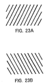
- Figs. 23A and 23 illustrate a state of an output of a highlight image
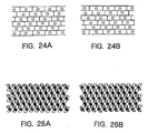
- Figs. 24A and 24B illustrate the configuration of the pixels for all of the colors and Fig. 24A illustrates that of the first color and Fig. 24B illustrates that of the second color.
- the recording density in the main scanning direction is 160 dpi (5/2 pixel corresponds to 1 dot) and that in the sub-scanning direction is 400 dpi (1 pixel corresponds to 1 dot).
- the image forming angle is arranged to be 26.6° for the first color and -26.6° for the second color.
- the resolution of the pattern signal generator 335 is arranged to be 200 dpi so that a pattern signal (triangular wave) as shown in Figs. 25A and 25B is generated.
- the pattern signal (triangular wave) is delayed for each of the scanning lines by a quantity of delay as follows: the quantity of delay of the triangular wave for each of the colors is 4/5 dot for the first color and 1/5 dot for the second color.
- the pixels for the colors are successively arranged to respectively form substantially elongated shapes. Therefore, the overlapped pixels in the form of the substantially elongated shape effect to prevent the long period deterioration while maintaining the effects of the above-described halftone dot printing technology. Furthermore, a multicolor image without color tone change can be obtained regardless of the quantity of the small color deviations and large color deviations generated due to the multiplication of the colors since the area of the overlapped portion is not changed as shown in Figs. 26A and 26B.
- the pixels are positioned adjacently to one another and are in the form of substantially the elongated shape, the side lobes of the light quantity distribution interfere with each other between the pixels. Therefore, even if the pixels are undesirably deviated, a further linearly formed image can easily be formed in comparison to isolated pixels positioned at constant intervals from the adjacent pixels as shown in Fig. 11. Therefore, the image deterioration for a short period such as the diagonal lines and the irregular pitch can be prevented.
- a pattern in which the image forming angle for the first color is 26.6° and that for the second color is -26.6° can be obtained by arranging the resolution of the pattern signal generator 335 to be 300 dpi, the quantity of delay of the triangular wave for the first color to be 1/4 dot and that for the second color to be 3/4 dot.
- each angle is arranged to be symmetrical with respect to the center line according to the above-described examples, a variety of combinations may be employed such that either of them is arranged to be 0° and another one is arranged to be 45°.
- the pulse width modulation circuit is used, the above examples are not not limited to this.
- the above examples can similarly be applied to an LBP (Laser Beam Printer) which uses a threshold matrix.
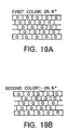
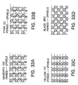
- Figs. 28A to 28C illustrate examples of the threshold matrix, wherein a matrix of 6 x 6 is used as the basic matrix and one pixel corresponds to 400 dpi x 400 dpi.
- Fig. 28A illustrates the matrix corresponding to the first color
- Fig. 28B illustrates that corresponding to the second color
- Fig. 28C illustrates that corresponding to the third color.
- the threshold matrix enables the pattern in which the pixels are disposed in the substantially elongated shape to be obtained similarly to the above-described examples.
- Figs. 28D to 28F illustrate the results of the output from the pixels corresponding to the matrices shown in Figs. 28A to 28C.
- a substantially elongated image is formed as shown in Figs. 28D to 28F.
- the irregular pitch and the irregular color can be prevented between the first and the second colors, between the second and the third colors and between the third and the first colors.
- the threshold matrices are not limited to those shown in Figs. 28A to 28C. Any pattern capable of forming the output image in the form of an elongated shape can, of course, be employed.
- the irregular pitch can be generated due to the visibility characteristics.
- Yellow does not generate an excessive irregular-pitch.
- the color deviation can be generated due to mechanical characteristics.
- the first and the fourth colors generate the color deviation from the second and the third colors.
- the structures arranged to use two or more color are to overcome at least either of the above-described two problems in terms of the deviation. For example, if any one of the four colors encounters the problem in terms of the deviation, the subject color suffering from the problem and other three colors are arranged to have different patterns to form the image. That is, if any one of the colors encounters problem, the elongated shape according to the above examples is arranged to be different in the image forming angle between the subject pixels and pixels for the other three colors.
- Figs. 51A to 51D illustrate an example of forming substantially elongated full color image. As shown in Figs. 51A to 51D, Yellow does not generate the excessive irregular pitch. However, the other three colors, that is, Magenta, Cyan and Black generate the irregular pitch respectively.
- the pixels are positioned adjacently to each other and in the form of the substantially elongated shape in a predetermined direction, a multicolor overlapped image without the image quality deterioration such as the irregular color, the irregular pitch and undesirable nonuniform lines can be stably formed.
- a color image forming apparatus which can be used in a laser beam printer is provided.
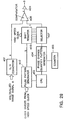
- Fig. 29 is a block diagram which illustrates the second embodiment of the color image forming apparatus according to the present invention.
- reference numeral 401 represents a D/A converter for converting the digital color image signal into an analog signal.
- Reference numeral 402 represents a pulse pattern generator for generating a pulse pattern for use in the pulse modulation of the analog color image signal.
- Reference numeral 408 represents a comparator for performing the pulse width modulation by making a comparison between the analog color image signal transmitted from the D/A converter 401 and the pulse pattern transmitted from the pulse pattern generator 402.
- Reference numeral 409 represents an amplifier for amplifying a PWM signal transmitted from the comparator 408.
- Reference numeral 406 represents a shift register for delaying the pulse pattern generated by the pulse pattern generator 402.
- Reference numeral 407 represents a selector for selecting a delay pattern formed by the shift register 406 in accordance with the pattern transmitted from a phase change quantity pattern generator 404 to be described later.
- the unit of the quantity of delay is arranged to be a delay of 1/4 pixel in a case where the reference unit of the PWM is arranged in such a manner that one unit is composed of two pixels. Therefore, 8 types of PWM patterns are formed due to the delay of the shift register 405. Therefore, the selector 7 is a circuit for selecting a delay pattern from the 8 types of the delay patterns formed by the shift register 406 so as to output the selected one.
- the selector 407 delays by D M pixel for each line in the case of M (Magenta), delays by D Y pixel for each line in the case of Y (Yellow), delays by D C pixel for each line in the case of C (Cyan) and delays by D BK pixel for each line in the case of Bk (Black).
- Reference numeral 405 represents a counter for counting a horizontal synchronizing signal.
- the counter 405 is a circuit for repeatedly counting the horizontal signals from “1" to “8” in such a manner that the same is counted up to “8” the counting is again started from “1".
- Reference numeral 404 represents a phase change quantity pattern generator which comprises, for example, a RAM which stores patterns for the corresponding colors.
- the phase change quantity pattern generator 404 transmits the result of the counting and the pattern formed in accordance with a control signal transmitted from a CPU 403 to be described later to the selector 407.
- Reference numeral 403 represents the CPU which transmits pattern signal for the corresponding colors to the pulse pattern generator 402 so as to control the final output from the selector 407. Furthermore, the CPU 403 controls the generation of the pattern signal in the phase change quantity pattern generator 404.
- the color components of the multicolor image signal (four types of digital signals for M, C, Y and Bk according to this embodiment) are successively converted into an analog signal a by the D/A converter 401.
- a reference signal b (according to this embodiment, it is a triangular wave) determined for each color component is processed under a control of the CPU 403 by utilizing a clock divided from a high speed clock by a pulse pattern generator 402. The reference signal b is then supplied to the shift register 406 so as to be delayed.
- the reference signal b is delayed by the shift register 406 in accordance with the 8 patterns before the selector 407 selects any one of the delayed reference signal so as to transmit it as a reference signal c.
- the reference signal c is subjected to a comparison with the analog signal a by the comparator 408 so that a PWM signal d is generated.
- the PWM signal d is amplified by the amplifier 409 so as to be transmitted as a processed signal B.
- a laser semiconductor (omitted form illustration) is operated so that an image is formed by the electronic photography method. The above-described operation is performed for each of the color components so that the colors are overlapped.
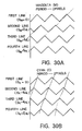
- Figs. 30A to 30D are waveform drawings which illustrate examples of the reference signal (triangular wave) for M, C, Y and Bk.
- the triangular signals for use at the time of forming an image of Magenta (M) has, as shown in Fig. 30A, a referential period (two pixels) serving as a reference.
- the triangular signal for use at the time of forming the Cyan (C) image has a reference period (two pixels) so that the delay quantity Dc for each of the first to the fourth lines is arranged to be 0, 6/4, 4/4 and 2/4.
- the triangular signal for use at the time of forming the Yellow (Y) image has a period (three pixels) which is 1.5 times the reference period.
- the delay quantity D Y is arranged to be "0" for all of the lines.
- the triangular signal for use at the time of forming the Black (Bk) image has a reference period (two pixels).
- the delay quantity D BK is arranged to be "0" for the odd number lines and 6/4 for the even number lines.
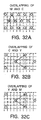
- Figs. 32A to 32C illustrate only the overlapped dots when two different dots are overlapped.
- the overlapped dots at the positions to be recorded when M and C are overlapped are shown in Fig. 32A.
- the three adjacent overlapped dots are positioned at the verteces of a substantially equilateral triangle.
- the overlapped dots when C and Y are overlapped or Y and M are overlapped are, as shown in Fig. 32C, positioned in such a manner that the three adjacent overlapped dots are positioned at the verteces of a substantially equilateral triangle.
- the overlapped dots and the non-overlapped dots are generated in a short period. Therefore, the long period irregular color due to the irregular rotation of the polygonal mirror can be prevented. As a result, even if the color deviation (deviation of the resist) takes place, the color tone change can be prevented.
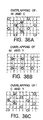
- This arrangement can also be used in such a manner that the positions of the dots of M, C, Y and Bk are arranged as shown in Figs. 33A to 33D.
- the apparatus see Fig. 29
- the contents of the phase change quantity pattern generator 404 must be reloaded.
- the overlapped dots when M and C, M and Y, and C and Y are overlapped are positioned at the verteces of a square as shown in Figs. 34A to 34C.
- a second modification is arranged in such a manner that dots having different color components are arranged as shown in Figs. 35A to 35C.
- the overlapped dots of the M and C, M and Y and C and Y are as shown in Figs. 36A to 36C.
- the overlapped dots are positioned at the verteces of a substantially eqilateral triangle.
- the overlapped dots are positioned at the verteces of a square.
- the full color image is formed.
- the present invention can be applied to a case in which the image is formed by two colors such as Black and red.
- the image may be formed at the period and the phase of the dots of the optional two color components among all of the colors to be recorded according to the above-described embodiments.
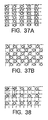
- structures may be employed in which the period and the phase of the pixels to be recorded are arranged to be as shown in Figs. 37A, 37B, 39A and 39B. The overlapped dots in these cases are shown in Figs. 38 and 40.
- the image is repeatedly formed at a plurality of phases for each of the lines for each of the color components. Furthermore, the period of the dots for the corresponding colors are determined so as to periodically position the overlapped dots for at least one line. Therefore, the overlapped dots are periodically positioned in the longitudinal and the lateral directions. That is, the dots on which a plurality of colors overlap and the pixels on which no pixel overlaps are periodically generated. Therefore, if a positional deviation is taken place for one color component, the overlapped dot and the non-overlapped dot are deviated from each other, causing no change in the color tone to be generated. Furthermore, since the overlapped dots and the non-overlapped dots are generated in a short period, the long period irregular color can be prevented.
- a modulation method such as the PWM is employed.
- the present invention is not limited to this.
- the present invention may, of course, be employed in an LBP printer or an LED printer which use the brightness modulation.
- the combination of the period of the reference signal and the delay quantity of the reference signal for each lines is changed for each of the colors so as to place the plurality of adjacent dots of the overlapped dots at the position to be recorded at the verteces of a substantially regular polygon for at least two color components. Therefore, the irregular color and the color deviation can be prevented and the color tone change for each print can also be prevented. As a result, a stable image can always be formed.
Landscapes
- Engineering & Computer Science (AREA)
- Multimedia (AREA)
- Signal Processing (AREA)
- Color, Gradation (AREA)
- Color Electrophotography (AREA)
- Facsimile Image Signal Circuits (AREA)
- Color Image Communication Systems (AREA)
Claims (18)
- Farbbildverarbeitungsgerät, mit:gekennzeichnet durch:einem Gliederungsmittel (408), das Intervalle zwischen Punktpositionen in Querrichtung entlang einer Abtastlinie zusammenstellt, auf der Punkte gebildet werden;einem Verschiebemittel (404; 406; 407) zum Verschieben der Punktpositionen in Querrichtung um einen Verschiebebetrag auf aufeinanderfolgenden Abtastzeilen bei aufeinanderfolgenden Längspositionen, wobei wenigstens eines der Intervalle und der Schiebebetrag für eine erste Farbkomponente von einem Intervall und einem Verschiebebetrag einer zweiten Farbkomponente verschieden sind, um ein Überlappungsmuster und nichtüberlappende Punkte zu bilden, in denen die Überlappungspunkte periodisch in Längs- und Querrichtung positioniert sind;ein Steuermittel (403) zum Steuern des Gliederungsmittels und des Verschiebemittels zum Bereitstellen des Musters in der Weise, daß benachbarte Überlappungspunkte ein Muster mit zwei Bildschirmwinkeln bilden, die relativ zur Längs- und Querrichtung schräg verlaufen.
- Gerät nach Anspruch 1, das des weiteren über einen Mustersignalgenerator (402) verfügt, um ein Mustersignal zu erzeugen, und über einen impulsbreitenmodulierten Bilddatengenerator (408, 409) zum Erzeugen von impulsbreitenmodulierten Bilddaten gemäß dem Mustersignal und einem Pixeldichtepegel;
wobei das Gliederungsmittel betriebsbereit ist, eine Periode des Mustersignals so zu steuern, daß die Intervalle zwischen den Positionen auf jeder Abtastzeile für jede Farbkomponente zusammenstellt sind und das Verschiebemittel betriebsbereit ist, die Phase des Mustersignals so zu steuern, daß die Verschiebung in den Punktpositionen auf jeder Abtastzeile bereitsteht. - Gerät nach Anspruch 2, dessen Mustersignal ein Dreieckswellensignal hat.
- Gerät nach einem der vorstehenden Ansprüche, das des weiteren ausgestattet ist mit
einem Mittel (401) zum Bestimmen des Pixeldichtepegels durch Umsetzen eingegebener Digitalbilddaten in Analogbilddaten. - Gerät nach einem der vorstehenden Ansprüche, das des weiteren über eine Bilderzeugungseinheit verfügt.
- Gerät nach Anspruch 5, dessen Bilderzeugungseinheit betriebsbereit ist, ein Bild auf einem Aufzeichnungsmedium unter Verwendung elektronischer Photographie zu erzeugen.
- Gerät nach Anspruch 6, dessen Bilderzeugungseinheit über einen Laserstrahldrucker mit einem Mittel zum Modulieren des Laserstrahls auf der Grundlage einer jeden Farbkomponente von impulsbreitenmodulierten Bilddaten verfügt.
- Gerät nach einem der vorstehenden Ansprüche, dessen Verschiebemittel betriebsbereit ist, die Punktpositionen auf jeder Abtastzeile um einen Betrag zu verschieben, der kleiner als eine Pixelgröße ist.
- Gerät nach einem der vorstehenden Ansprüche, bei dem sowohl die erste Farbkomponente als auch die zweite Farbkomponente chromatische Farbkomponenten enthalten.
- Mehrfarbenbilderzeugungsverfahren, mit den Verfahrensschritten:gekennzeichnet durchGliedern von Intervallen zwischen Punktpositionen in Querrichtung entlang einer Abtastzeile, auf der Punkte erzeugt werden;Verschieben der Punktpositionen in Querrichtung um einen Verschiebebetrag auf aufeinanderfolgenden Abtastzeilen bei aufeinanderfolgenden Längspositionen, wobei wenigstens eines der Intervalle und der Schiebebetrag für eine erste Farbkomponente von einem Intervall und einem Verschiebebetrag einer zweiten Farbkomponente verschieden sind, um ein Überlappungsmuster und nichtüberlappende Punkte zu bilden, in denen die Überlappungspunkte periodisch in Längs- und Querrichtung positioniert sind;Steuern des Gliederungsschrittes und des Verschiebeschrittes zum Bereitstellen des Musters in der Weise, daß benachbarte Überlappungspunkte ein Muster mit zwei Bildschirmwinkeln bilden, die relativ zur Längs- und Querrichtung schräg verlaufen.
- Verfahren nach Anspruch 10, mit dem weiteren Verfahrensschritt des Erzeugens eines Mustersignals und des Erzeugens von impulsbreitenmodulierten Bilddaten gemäß dem Mustersignal und einem Pixeldichtepegel;
wobei das Steuern der Periode des Mustersignals bewirkt, daß die Intervalle zwischen den Punktpositionen auf jeder Abtastzeile für jede Farbkomponente gliedert und die Phase des Mustersignals die Verschiebung in den Punktpositionen auf jeder Abtastzeile herbeiführt. - Verfahren nach Anspruch 11, dessen Mustersignal ein Dreieckswellensignal hat.
- Verfahren nach einem der Ansprüche 10 bis 12, mit dem weiteren Verfahrensschritt des Bestimmens vom Pixeldichtepegel durch Umsetzen von eingegebenen Digitalbilddaten in Analogbilddaten.
- Verfahren nach einem der Ansprüche 10 bis 13, mit dem weiteren Verfahrensschritt des Abgebens der Bilddaten an eine Bilderzeugungseinheit.
- Verfahren nach Anspruch 14, dessen Bilderzeugungseinheit ein Bild auf einem Aufzeichnungsmedium unter Verwendung elektronischer Photographie erzeugt.
- Verfahren nach Anspruch 15, dessen Bilderzeugungsgerät einen Laserstrahldrucker enthält, der einen Laserstrahl auf der Grundlage einer jeden Farbkomponente von impulsbreitenmodulierten Bilddaten moduliert.
- Verfahren nach einem der Ansprüche 10 bis 16, bei dem die geänderten Beträge der Phasenverschiebung die Punktpositionen auf jeder Abtastzeile um einen Betrag verschieben, der kleiner als eine Pixelgröße ist.
- Verfahren nach einem der Ansprüche 10 bis 17, bei dem die erste Farbkomponente und die zweite Farbkomponente chromatische Farbkomponenten haben.
Applications Claiming Priority (11)
| Application Number | Priority Date | Filing Date | Title |
|---|---|---|---|
| JP2008370A JPH03214864A (ja) | 1990-01-19 | 1990-01-19 | カラー画像処理装置 |
| JP837090 | 1990-01-19 | ||
| JP1655590 | 1990-01-26 | ||
| JP1655590A JP2911511B2 (ja) | 1990-01-26 | 1990-01-26 | 多色画像形成装置 |
| JP1656190 | 1990-01-26 | ||
| JP2016561A JP2911512B2 (ja) | 1990-01-26 | 1990-01-26 | 多色画像形成方法 |
| JP2223890 | 1990-02-02 | ||
| JP2022238A JPH03228471A (ja) | 1990-02-02 | 1990-02-02 | カラー画像処理装置 |
| JP18177190A JP3156183B2 (ja) | 1990-07-10 | 1990-07-10 | 多色画像形成方法 |
| JP18177190 | 1990-07-10 | ||
| EP91300293A EP0438271B1 (de) | 1990-01-19 | 1991-01-16 | Farbbildverarbeitungsanordnung |
Related Parent Applications (1)
| Application Number | Title | Priority Date | Filing Date |
|---|---|---|---|
| EP91300293A Division EP0438271B1 (de) | 1990-01-19 | 1991-01-16 | Farbbildverarbeitungsanordnung |
Publications (3)
| Publication Number | Publication Date |
|---|---|
| EP0959615A2 EP0959615A2 (de) | 1999-11-24 |
| EP0959615A3 EP0959615A3 (de) | 2000-07-12 |
| EP0959615B1 true EP0959615B1 (de) | 2005-03-16 |
Family
ID=27518936
Family Applications (2)
| Application Number | Title | Priority Date | Filing Date |
|---|---|---|---|
| EP91300293A Expired - Lifetime EP0438271B1 (de) | 1990-01-19 | 1991-01-16 | Farbbildverarbeitungsanordnung |
| EP99202644A Expired - Lifetime EP0959615B1 (de) | 1990-01-19 | 1991-01-16 | Farbbildverarbeitungsgerät |
Family Applications Before (1)
| Application Number | Title | Priority Date | Filing Date |
|---|---|---|---|
| EP91300293A Expired - Lifetime EP0438271B1 (de) | 1990-01-19 | 1991-01-16 | Farbbildverarbeitungsanordnung |
Country Status (3)
| Country | Link |
|---|---|
| US (2) | US5469266A (de) |
| EP (2) | EP0438271B1 (de) |
| DE (2) | DE69133449T2 (de) |
Families Citing this family (24)
| Publication number | Priority date | Publication date | Assignee | Title |
|---|---|---|---|---|
| JPH06155815A (ja) * | 1992-11-18 | 1994-06-03 | Konica Corp | 画像形成装置 |
| US5786900A (en) * | 1994-03-23 | 1998-07-28 | Fuji Photo Film Co., Ltd. | Image recording device for recording multicolor images with dot pitch pattern randomly arranged only in the sub-scanning direction |
| JP2815087B2 (ja) * | 1994-07-07 | 1998-10-27 | 富士ゼロックス株式会社 | 多色画像形成装置及び方法 |
| DE69531142T2 (de) * | 1994-12-28 | 2004-05-13 | Fuji Photo Film Co., Ltd., Minami-Ashigara | Bildaufzeichnungsverfahren |
| JPH09261469A (ja) * | 1996-01-19 | 1997-10-03 | Canon Inc | 画像処理装置及び画像処理方法 |
| US5796929A (en) * | 1996-10-24 | 1998-08-18 | Seiko Epson Corporation | Banding and ink-bleeding reduction in cluster dither by screen displacement |
| US6404510B1 (en) * | 1997-05-28 | 2002-06-11 | Fuji Photo Film Co., Ltd. | Image printing method |
| JPH1141473A (ja) * | 1997-07-15 | 1999-02-12 | Toshiba Corp | 画像処理装置と画像記録装置と画像形成装置 |
| JP3950522B2 (ja) | 1997-09-12 | 2007-08-01 | キヤノン株式会社 | 画像処理装置及び画像処理方法 |
| US6236415B1 (en) | 1997-12-24 | 2001-05-22 | Canon Kabushiki Kaisha | Image forming apparatus and control method therefor |
| US6166821A (en) * | 1998-10-02 | 2000-12-26 | Electronics For Imaging, Inc. | Self calibrating pulse width modulator for use in electrostatic printing applications |
| US6307645B1 (en) * | 1998-12-22 | 2001-10-23 | Xerox Corporation | Halftoning for hi-fi color inks |
| US6633412B1 (en) | 1999-03-26 | 2003-10-14 | Seiko Epson Corporation | Smoothness enhancement in laser printing through periodic modulation of halftone cell |
| JP2001219599A (ja) * | 2000-02-10 | 2001-08-14 | Alps Electric Co Ltd | 画像形成方法 |
| US6326993B1 (en) * | 2000-03-15 | 2001-12-04 | Toshiba Tec Kabushiki Kaisha | Pulse width modulation system and image forming apparatus having the pulse width modulation system |
| JP3937906B2 (ja) * | 2001-05-07 | 2007-06-27 | キヤノン株式会社 | 画像表示装置 |
| US6712442B1 (en) | 2002-09-23 | 2004-03-30 | Lexmark International, Inc. | Method of image rasterization and imaging an address space an ink jet printers |
| JP4065533B2 (ja) * | 2003-05-16 | 2008-03-26 | キヤノン株式会社 | 変調装置 |
| JP4682770B2 (ja) * | 2005-09-21 | 2011-05-11 | 富士ゼロックス株式会社 | 画像形成装置 |
| JP4756597B2 (ja) * | 2005-11-09 | 2011-08-24 | 株式会社リコー | 画像形成装置および方法 |
| JP4545719B2 (ja) * | 2006-07-29 | 2010-09-15 | 株式会社リコー | 画像読取信号処理icおよび画像読取装置と画像形成装置 |
| US20090309682A1 (en) * | 2008-06-13 | 2009-12-17 | Northrop Grumman Guidance And Electronic Company, Inc. | Eight-fold dipole magnet array for generating a uniform magnetic field |
| JP4752920B2 (ja) | 2009-01-22 | 2011-08-17 | ブラザー工業株式会社 | 画像処理装置及び画像処理プログラム |
| JP5751555B2 (ja) * | 2012-05-30 | 2015-07-22 | 株式会社沖データ | 画像読取装置及び複合装置 |
Family Cites Families (22)
| Publication number | Priority date | Publication date | Assignee | Title |
|---|---|---|---|---|
| US4149183A (en) * | 1976-05-21 | 1979-04-10 | Xerox Corporation | Electronic halftone generator |
| US4196451A (en) * | 1976-05-21 | 1980-04-01 | Xerox Corporation | Electronic halftone generator |
| US4185304A (en) * | 1977-07-07 | 1980-01-22 | Xerox Corporation | Electronic halftone screening |
| DE3312273C3 (de) * | 1982-04-06 | 1996-03-21 | Canon Kk | Bildverarbeitungsgerät |
| US4507685A (en) * | 1982-06-25 | 1985-03-26 | Canon Kabushiki Kaisha | Image recording device |
| EP0204094B2 (de) * | 1985-03-30 | 1998-08-19 | Hitachi, Ltd. | Druckverfahren vom Abtastaufzeichnungstyp und dessen Verwirklichungsvorrichtung |
| FR2584549B1 (fr) * | 1985-07-03 | 1990-08-31 | Commissariat Energie Atomique | Procede d'utilisation d'un registre binaire a n cellules bistables permettant de determiner le rapport de deux frequences et dispositif pour la mise en oeuvre du procede |
| US4800442A (en) * | 1985-08-15 | 1989-01-24 | Canon Kabushiki Kaisha | Apparatus for generating an image from a digital video signal |
| EP0213891B1 (de) * | 1985-08-20 | 1993-10-27 | Canon Kabushiki Kaisha | Bildverarbeitungsgerät |
| JP2710118B2 (ja) * | 1985-08-20 | 1998-02-10 | キヤノン株式会社 | 画像処理装置 |
| US4870499A (en) * | 1985-08-29 | 1989-09-26 | Canon Kabushiki Kaisha | Image processing apparatus |
| US4897734A (en) * | 1985-10-28 | 1990-01-30 | Canon Kabushiki Kaisha | Image processing apparatus |
| JPH0795805B2 (ja) * | 1986-02-07 | 1995-10-11 | キヤノン株式会社 | 画像処理装置 |
| JPH0795806B2 (ja) * | 1986-02-07 | 1995-10-11 | キヤノン株式会社 | 画像処理装置 |
| JPH0828815B2 (ja) * | 1986-02-07 | 1996-03-21 | キヤノン株式会社 | 画像処理装置 |
| JPS62198266A (ja) * | 1986-02-26 | 1987-09-01 | Canon Inc | カラ−画像情報処理装置 |
| JPS62230163A (ja) * | 1986-03-31 | 1987-10-08 | Canon Inc | 画像処理装置 |
| US4868684A (en) * | 1986-04-03 | 1989-09-19 | Canon Kabushiki Kaisha | Image processing apparatus |
| US4974067A (en) * | 1986-06-06 | 1990-11-27 | Ricoh Company, Ltd. | Multi-step-digital color image reproducing method and apparatus |
| US4918622A (en) * | 1988-11-16 | 1990-04-17 | Eastman Kodak Company | Electronic graphic arts screener |
| US5172132A (en) * | 1990-03-06 | 1992-12-15 | Konica Corporation | Digital image forming device and method for forming an image from a plurality of dots |
| EP0528618B1 (de) * | 1991-08-21 | 1996-11-06 | Konica Corporation | Abbildungsgerät |
-
1991
- 1991-01-16 EP EP91300293A patent/EP0438271B1/de not_active Expired - Lifetime
- 1991-01-16 DE DE69133449T patent/DE69133449T2/de not_active Expired - Fee Related
- 1991-01-16 DE DE69132230T patent/DE69132230T2/de not_active Expired - Fee Related
- 1991-01-16 EP EP99202644A patent/EP0959615B1/de not_active Expired - Lifetime
-
1994
- 1994-06-13 US US08/259,123 patent/US5469266A/en not_active Expired - Lifetime
-
1995
- 1995-06-07 US US08/477,643 patent/US5748328A/en not_active Expired - Lifetime
Also Published As
| Publication number | Publication date |
|---|---|
| DE69132230D1 (de) | 2000-07-06 |
| EP0959615A2 (de) | 1999-11-24 |
| EP0959615A3 (de) | 2000-07-12 |
| DE69132230T2 (de) | 2000-11-09 |
| DE69133449T2 (de) | 2005-09-15 |
| DE69133449D1 (de) | 2005-04-21 |
| US5469266A (en) | 1995-11-21 |
| US5748328A (en) | 1998-05-05 |
| EP0438271A2 (de) | 1991-07-24 |
| EP0438271B1 (de) | 2000-05-31 |
| EP0438271A3 (en) | 1993-04-07 |
Similar Documents
| Publication | Publication Date | Title |
|---|---|---|
| EP0959615B1 (de) | Farbbildverarbeitungsgerät | |
| JPH0716234B2 (ja) | カラープリンタ | |
| US5283658A (en) | Image forming apparatus with TTL to ECL conversion between reading and printing circuits | |
| JPH11212009A (ja) | マルチビーム記録装置 | |
| US6342953B1 (en) | Color plane under exposure for reducing edge effect | |
| US7196804B2 (en) | Image processing apparatus and method, and storage medium used therewith | |
| US6512534B2 (en) | Clock control apparatus and method and image forming apparatus using clock control apparatus | |
| US20020085217A1 (en) | Image processing apparatus and image processing system | |
| US6791713B1 (en) | Image forming apparatus | |
| US5541736A (en) | Color image forming system which conducts charging exposure and development with respect to a photosensitive medium at a plurality of times | |
| EP0901277B1 (de) | Bildverarbeitungsvorrichtung und -verfahren | |
| JP3471832B2 (ja) | 画像形成装置及び方法 | |
| JP4209704B2 (ja) | 画像形成装置、画像形成方法 | |
| JPH08300730A (ja) | 画像形成装置 | |
| US7315712B2 (en) | Electrophotographic image recording apparatus and method therefore | |
| JPH07254986A (ja) | 画像形成装置 | |
| JPS62296660A (ja) | ビ−ム走査装置 | |
| JP3156183B2 (ja) | 多色画像形成方法 | |
| JPH0918731A (ja) | 画像処理装置 | |
| JP3204049B2 (ja) | 多色画像形成装置 | |
| JP2911511B2 (ja) | 多色画像形成装置 | |
| JPH1127552A (ja) | カラー画像の階調処理装置及び階調処理方法 | |
| JPH091855A (ja) | 画像処理装置 | |
| JP2002113902A (ja) | 画像形成装置 | |
| JP2800501B2 (ja) | 画像形成装置 |
Legal Events
| Date | Code | Title | Description |
|---|---|---|---|
| PUAI | Public reference made under article 153(3) epc to a published international application that has entered the european phase |
Free format text: ORIGINAL CODE: 0009012 |
|
| AC | Divisional application: reference to earlier application |
Ref document number: 438271 Country of ref document: EP |
|
| AK | Designated contracting states |
Kind code of ref document: A2 Designated state(s): DE FR GB IT |
|
| RIN1 | Information on inventor provided before grant (corrected) |
Inventor name: YAMADA, MASANORI Inventor name: ARIMOTO, SHINOBU Inventor name: NAGASE, YUKIO Inventor name: KEMMOCHI, KAZUHISA Inventor name: IKEDA, YOSHINORI Inventor name: YOSHIZAWA, ATSUTOMO Inventor name: MOCHIDA, YOSHINORI Inventor name: USAMI, AKIHIRO |
|
| RIC1 | Information provided on ipc code assigned before grant |
Free format text: 7H 04N 1/52 A |
|
| RIN1 | Information on inventor provided before grant (corrected) |
Inventor name: YAMADA, MASANORI Inventor name: ARIMOTO, SHINOBU Inventor name: NAGASE, YUKIO Inventor name: KEMMOCHI, KAZUHISA Inventor name: IKEDA, YOSHINORI Inventor name: YOSHIZAWA, ATSUTOMO Inventor name: MOCHIDA, YOSHINORI Inventor name: USAMI, AKIHIRO |
|
| PUAL | Search report despatched |
Free format text: ORIGINAL CODE: 0009013 |
|
| AK | Designated contracting states |
Kind code of ref document: A3 Designated state(s): DE FR GB IT |
|
| 17P | Request for examination filed |
Effective date: 20001127 |
|
| AKX | Designation fees paid |
Free format text: DE FR GB IT |
|
| 17Q | First examination report despatched |
Effective date: 20020408 |
|
| GRAP | Despatch of communication of intention to grant a patent |
Free format text: ORIGINAL CODE: EPIDOSNIGR1 |
|
| GRAS | Grant fee paid |
Free format text: ORIGINAL CODE: EPIDOSNIGR3 |
|
| GRAA | (expected) grant |
Free format text: ORIGINAL CODE: 0009210 |
|
| AC | Divisional application: reference to earlier application |
Ref document number: 0438271 Country of ref document: EP Kind code of ref document: P |
|
| AK | Designated contracting states |
Kind code of ref document: B1 Designated state(s): DE FR GB IT |
|
| REG | Reference to a national code |
Ref country code: GB Ref legal event code: FG4D |
|
| REF | Corresponds to: |
Ref document number: 69133449 Country of ref document: DE Date of ref document: 20050421 Kind code of ref document: P |
|
| PLBE | No opposition filed within time limit |
Free format text: ORIGINAL CODE: 0009261 |
|
| STAA | Information on the status of an ep patent application or granted ep patent |
Free format text: STATUS: NO OPPOSITION FILED WITHIN TIME LIMIT |
|
| 26N | No opposition filed |
Effective date: 20051219 |
|
| ET | Fr: translation filed | ||
| PGFP | Annual fee paid to national office [announced via postgrant information from national office to epo] |
Ref country code: DE Payment date: 20090131 Year of fee payment: 19 |
|
| PGFP | Annual fee paid to national office [announced via postgrant information from national office to epo] |
Ref country code: GB Payment date: 20090127 Year of fee payment: 19 |
|
| PGFP | Annual fee paid to national office [announced via postgrant information from national office to epo] |
Ref country code: IT Payment date: 20090119 Year of fee payment: 19 |
|
| PGFP | Annual fee paid to national office [announced via postgrant information from national office to epo] |
Ref country code: FR Payment date: 20090121 Year of fee payment: 19 |
|
| GBPC | Gb: european patent ceased through non-payment of renewal fee |
Effective date: 20100116 |
|
| REG | Reference to a national code |
Ref country code: FR Ref legal event code: ST Effective date: 20100930 |
|
| PG25 | Lapsed in a contracting state [announced via postgrant information from national office to epo] |
Ref country code: FR Free format text: LAPSE BECAUSE OF NON-PAYMENT OF DUE FEES Effective date: 20100201 |
|
| PG25 | Lapsed in a contracting state [announced via postgrant information from national office to epo] |
Ref country code: DE Free format text: LAPSE BECAUSE OF NON-PAYMENT OF DUE FEES Effective date: 20100803 |
|
| PG25 | Lapsed in a contracting state [announced via postgrant information from national office to epo] |
Ref country code: GB Free format text: LAPSE BECAUSE OF NON-PAYMENT OF DUE FEES Effective date: 20100116 |
|
| PG25 | Lapsed in a contracting state [announced via postgrant information from national office to epo] |
Ref country code: IT Free format text: LAPSE BECAUSE OF NON-PAYMENT OF DUE FEES Effective date: 20100116 |