EP0957405B1 - Bildherstellungsapparat - Google Patents
Bildherstellungsapparat Download PDFInfo
- Publication number
- EP0957405B1 EP0957405B1 EP99109499A EP99109499A EP0957405B1 EP 0957405 B1 EP0957405 B1 EP 0957405B1 EP 99109499 A EP99109499 A EP 99109499A EP 99109499 A EP99109499 A EP 99109499A EP 0957405 B1 EP0957405 B1 EP 0957405B1
- Authority
- EP
- European Patent Office
- Prior art keywords
- photosensitive member
- thickness
- temperature
- heater
- conductive substrate
- Prior art date
- Legal status (The legal status is an assumption and is not a legal conclusion. Google has not performed a legal analysis and makes no representation as to the accuracy of the status listed.)
- Expired - Lifetime
Links
Images


Classifications
-
- G—PHYSICS
- G03—PHOTOGRAPHY; CINEMATOGRAPHY; ANALOGOUS TECHNIQUES USING WAVES OTHER THAN OPTICAL WAVES; ELECTROGRAPHY; HOLOGRAPHY
- G03G—ELECTROGRAPHY; ELECTROPHOTOGRAPHY; MAGNETOGRAPHY
- G03G15/00—Apparatus for electrographic processes using a charge pattern
- G03G15/75—Details relating to xerographic drum, band or plate, e.g. replacing, testing
- G03G15/751—Details relating to xerographic drum, band or plate, e.g. replacing, testing relating to drum
-
- G—PHYSICS
- G03—PHOTOGRAPHY; CINEMATOGRAPHY; ANALOGOUS TECHNIQUES USING WAVES OTHER THAN OPTICAL WAVES; ELECTROGRAPHY; HOLOGRAPHY
- G03G—ELECTROGRAPHY; ELECTROPHOTOGRAPHY; MAGNETOGRAPHY
- G03G5/00—Recording-members for original recording by exposure, e.g. to light, to heat or to electrons; Manufacture thereof; Selection of materials therefor
- G03G5/02—Charge-receiving layers
- G03G5/04—Photoconductive layers; Charge-generation layers or charge-transporting layers; Additives therefor; Binders therefor
- G03G5/08—Photoconductive layers; Charge-generation layers or charge-transporting layers; Additives therefor; Binders therefor characterised by the photoconductive material being inorganic
- G03G5/082—Photoconductive layers; Charge-generation layers or charge-transporting layers; Additives therefor; Binders therefor characterised by the photoconductive material being inorganic and not being incorporated in a bonding material, e.g. vacuum deposited
- G03G5/08214—Silicon-based
- G03G5/08221—Silicon-based comprising one or two silicon based layers
-
- G—PHYSICS
- G03—PHOTOGRAPHY; CINEMATOGRAPHY; ANALOGOUS TECHNIQUES USING WAVES OTHER THAN OPTICAL WAVES; ELECTROGRAPHY; HOLOGRAPHY
- G03G—ELECTROGRAPHY; ELECTROPHOTOGRAPHY; MAGNETOGRAPHY
- G03G5/00—Recording-members for original recording by exposure, e.g. to light, to heat or to electrons; Manufacture thereof; Selection of materials therefor
- G03G5/02—Charge-receiving layers
- G03G5/04—Photoconductive layers; Charge-generation layers or charge-transporting layers; Additives therefor; Binders therefor
- G03G5/08—Photoconductive layers; Charge-generation layers or charge-transporting layers; Additives therefor; Binders therefor characterised by the photoconductive material being inorganic
- G03G5/082—Photoconductive layers; Charge-generation layers or charge-transporting layers; Additives therefor; Binders therefor characterised by the photoconductive material being inorganic and not being incorporated in a bonding material, e.g. vacuum deposited
- G03G5/08214—Silicon-based
- G03G5/08278—Depositing methods
-
- G—PHYSICS
- G03—PHOTOGRAPHY; CINEMATOGRAPHY; ANALOGOUS TECHNIQUES USING WAVES OTHER THAN OPTICAL WAVES; ELECTROGRAPHY; HOLOGRAPHY
- G03G—ELECTROGRAPHY; ELECTROPHOTOGRAPHY; MAGNETOGRAPHY
- G03G5/00—Recording-members for original recording by exposure, e.g. to light, to heat or to electrons; Manufacture thereof; Selection of materials therefor
- G03G5/10—Bases for charge-receiving or other layers
- G03G5/102—Bases for charge-receiving or other layers consisting of or comprising metals
-
- G—PHYSICS
- G03—PHOTOGRAPHY; CINEMATOGRAPHY; ANALOGOUS TECHNIQUES USING WAVES OTHER THAN OPTICAL WAVES; ELECTROGRAPHY; HOLOGRAPHY
- G03G—ELECTROGRAPHY; ELECTROPHOTOGRAPHY; MAGNETOGRAPHY
- G03G5/00—Recording-members for original recording by exposure, e.g. to light, to heat or to electrons; Manufacture thereof; Selection of materials therefor
- G03G5/10—Bases for charge-receiving or other layers
- G03G5/104—Bases for charge-receiving or other layers comprising inorganic material other than metals, e.g. salts, oxides, carbon
Definitions
- the present invention relates to an image forming apparatus according to claim 1.
- the photoconductive material constituting the photoconductive layer in the image forming member for electrophotography is required, in the image formation field, to satisfy various characteristics such as a high sensitivity, a high S/N ratio (photocurrent (Ip)/(Id)), spectral absorption characteristics matching the spectral characteristics of the irradiating electromagnetic wave (light in wide sense including ultraviolet light, visible light, infrared light, X-ray, gamma-ray, etc.), a high-speed light response, a desired dark resistance and no pollution to the human body at use.
- the above-mentioned pollution-free property at use is particularly important in the case of the electrophotographic image forming member incorporated in the electrophotographic apparatus to be used as an office equipment in the office.
- amorphous silicon of which dangling bonds are bonded with monovalent elements such as hydrogen atoms (H) or halogen atoms (X) (hereinafter represented as "a-Si(H, X)") is described as to application to the electrophotographic image forming member, for example in DE-A- 2746967 and DE-A-2855718 , and is already utilized in the electrophotographic image forming member because it has excellent photoconductivity, abrasion resistance and heat resistance, and it is relatively easily formed with a large area.
- an electrophotographic photosensitive drum with a photoconductive material containing a-Si(H, X) in order to obtain satisfactory photoconductive characteristics, there is generally employed a method of continuously heating a drum-shaped metal substrate, in an a-Si(H, X) film deposition apparatus, at a temperature of 200°C to 350°C which is extremely higher than that in the case of a selenium-based drum, and depositing an a-Si(H, X) film with a thickness of 1 to 100 ⁇ m on the drum-shaped metal substrate.
- Such continued heating of the substrate at the high temperature is essential for obtaining the a-Si based photosensitive drum with excellent electrophotographic characteristics, and currently requires several hours to ten and several hours in consideration of the deposition rate of the a-Si(H, X) film.
- the electrophotographic photoconductive member is composed of a drum-shaped or cylindrical metal substrate composed of Al or an Al alloy (hereinafter referred to as Al-based substrate) constituting the metal support member for the electrophotographic photoconductive member, and a photoconductive layer formed on the drum-shaped Al-based metal substrate and having an amorphous material containing silicon atoms as a matrix and preferably at least one kind of hydrogen atoms and halogen atoms.
- the photoconductive layer may also be provided with a barrier layer in contact with the drum-shaped metal substrate and further a surface barrier layer on the surface of the photoconductive layer.
- Figs. 1A and 1B are views showing an example of the structure of the a-Si photosensitive member.
- Fig. 1A is a schematic perspective view of the photosensitive member, wherein reference numeral 2100 indicates the thickness of the photosensitive member including a substrate 2101 and a light-receiving layer 2103.
- Fig. 1B is a schematic cross-sectional view of the photosensitive member.
- a charge injection inhibition layer 2102 for inhibiting charge injection from the conductive substrate 2102
- a photoconductive layer 2103 for generating electrons and positive holes by light irradiation and converting image information into potential information.
- Each of these layers is composed of amorphous silicon as a matrix and, if necessary, further contains a dangling bond neutralizing agent such as halogen atoms or hydrogen atoms, a valence electron controlling agent such as an element of the group III or V of the periodic table, a modifying material such as oxygen, carbon or nitrogen atoms.
- a surface protective layer 2104 for protecting the photoconductive layer from the abrasion by a developer, a transfer paper and a cleaning device and for inhibiting the charge injection from the surface into the photoconductive layer.
- the surface protective layer 2104 is composed of a-SiC:H which is excellent in light transmission to the photoconductive layer, mechanical strength and prevention of charge injection from above.
- the material constituting the drum-shaped metal substrate is preferably composed of, for example a metal such as NiCr, stainless steel, Al, Cr, Mo, Au, Nb, Ta, V, Ti, Pt or Pd, or an alloy thereof, and particularly Al or an Al-based alloy is preferably used.
- a metal such as NiCr, stainless steel, Al, Cr, Mo, Au, Nb, Ta, V, Ti, Pt or Pd, or an alloy thereof, and particularly Al or an Al-based alloy is preferably used.
- the material of the drum-shaped substrate aluminum or aluminum-based alloy is preferred because satisfactory dimensional precision, for example in circularity or surface smoothness can be obtained relatively easily, also because the temperature control is relatively easy in the surface portion of the deposition of a-Si(H, X) at the manufacturing process and furthermore because such material is economical.
- the halogen atoms (X) that can be contained in the photoconductive layer of the photoconductive member include fluorine, chlorine, bromine and iodine, but preferred is chlorine and particularly fluorine.
- the photoconductive layer may further contain, as the aforementioned valence electron controlling material or modifying material, a component for regulating the Fermi level or the bandgap such as atoms belonging to the group III of the periodic table such as boron or gallium atoms (hereinafter referred to as "group III atoms”), atoms belonging to the group V of the periodic table such as nitrogen, phosphor or arsine atoms (hereinafter referred to as "group V atoms”), oxygen atoms, carbon atoms, germanium atoms, alone or in suitable combination.
- the barrier layer is provided for improving the adhesion between the photoconductive layer and the drum-shaped metal substrate or adjusting the charge receiving ability.
- the barrier layer is constructed with a single- or multi-layered structure composed of an a-Si(H, X) layer or a polycrystalline Si layer containing the group III atoms, group V atoms, oxygen atoms, carbon atoms, germanium atoms etc. according to the purpose.
- a surface charge injection inhibition layer or a protective layer consisting of an amorphous material containing silicon atoms as a matrix and carbon, nitrogen, oxygen atoms, etc. preferably in a large amount and, if necessary, further containing hydrogen or halogen atoms, or consisting of an organic substance with a high electric resistance.
- the photoconductive layer composed of a-Si(H, X) can be formed with conventional various vacuum deposition methods utilizing electric discharge phenomena such as a glow discharge method, a sputtering method or an ion plating method.
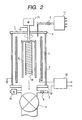
- FIG. 2 shows an example of the apparatus for producing the electrophotographic photosensitive member by the glow discharge deposition method.
- a deposition chamber 1 is composed of a base plate 2, a wall 3 and a top plate 4.
- a cylindrical cathode electrode 5 In the deposition chamber 1, there is provided a cylindrical cathode electrode 5, and a drum-shaped metal substrate 6 on which the a-Si(H, X) film is to be deposited.
- the substrate 6 is positioned at the central portion (concentric center) of the cathode electrode 5 and also functions as an anode electrode.
- a raw material gas introduction valve 7 and a leak valve 8 are at first closed, and a discharge valve 9 is opened to evacuate the interior of the deposition chamber 1.
- a vacuum gauge 10 indicates about 0,665 ⁇ 10 -3 Pa (5 ⁇ 10 -6 Torr)
- the raw material gas introduction valve 7 is opened to introduce, into the deposition chamber 1, mixed raw material gases such as SiH 4 , Si 2 H 6 , SiF 4 , etc. adjusted at a previously predetermined ratio in a mass flow controller 11.
- the opening degree of the discharge valve 9 is adjusted under the observation of the reading of the vacuum gauge 10, so as to maintain the pressure in the deposition chamber 1 at a predetermined value.
- a high frequency power source 13 is activated at a desired power to generate glow discharge in the deposition chamber 1.
- the drum-shaped metal substrate 6 is rotated at a constant speed by a motor (M) 14, in order to achieve uniform layer formation.
- M motor
- an a-Si(H, X) deposition film can be formed on the drum-shaped metal substrate 6.
- the deposited a-Si(H, X) film often peels off from the drum-shaped metal substrate not only during the film deposition in which the drum-shaped metal substrate is maintained at a high temperature but also during the cooling to the atmospheric temperature after the film deposition, because of a difference in the thermal expansion coefficient between the drum-shaped metal substrate and the a-Si(H, X) film and also because of a large internal stress in the formed a-Si(H, X) film.
- the peeling of the a-Si(H, X) film is often observed in the course of use as the electrophotographic photosensitive drum, by the heating of the drum depending on the ambient temperature in the use.
- Such peeling of the a-Si(H, X) film tends to occur more easily with an increase in the thickness thereof, and is also caused in the case of the a-Si(H, X)-based photosensitive drum.
- the film peeling often generates in the a-Si(H, X)-based photosensitive drum because of the difference in the thermal expansion coefficient as mentioned above and the large internal stress of the a-Si(H, X) film.
- the internal stress of the a-Si(H, X) film can be relaxed to a certain extent by the producing conditions of the a-Si(H, X) film (such as the kind of the raw material gasses, gas flow rate ratio, discharge power, substrate temperature, internal structure of the producing apparatus, etc.), but such relaxation is still insufficient in consideration of the productivity and mass production efficiency.
- the film peeling is fatal, inducing an image defect in the use of the electrophotographic photosensitive drum.
- the heating of the drum-shaped metal substrate at the high temperature for a long time in the production of the a-Si(H, X) film not only induces the film peeling as mentioned above but also tends to cause thermal deformation of the drum-shaped metal substrate.
- This thermal deformation causes uneven discharge in the production of the a-Si(H, X) film, thereby degrading the uniformity of the deposited film and resulting in an image defect.
- an electrophotographic photoconductive member capable of reducing the image defect by employing a drum-shaped metal substrate composed of aluminum or an aluminum alloy having a thickness of at least 2.5 mm.
- the raw material cost has a large proportion, and a reduction in the thickness of the drum-shaped metal substrate is anticipated not only to simply reduce the raw material cost but also, because of a low heat capacity resulting from the smaller thickness, to achieve various cost reduction effects such as electric power saving and a shorter tact time based on a shorter heating time, a reduction in the electric power required for maintaining the high temperature, and a reduction in the tact time based on a reduced cooling time in the production of the a-Si(H, X) film.
- a lower cost of the drum-shaped metal substrate and an improvement in the temperature characteristics thereof have been desired.
- JP-A-63-210864 discloses a generic image forming apparatus.
- This image forming apparatus comprises an electrophotographic photosensitive member (1) having a cylindrical shape, the electrophotographic photosensitive member comprises a conductive substrate; and a light-receiving layer (1b-1d) having a photoconductive layer on the conductive substrate, the light-receiving layer containing at least amorphous silicon, wherein the photoconductive layer has a thickness not smaller than 10 ⁇ m and smaller or equal than 20 ⁇ m, the image forming apparatus further comprising a charging device (2) for charging the photosensitive member (1), wherein the charging device is a device for contacting a cylindrical charging member (21) with a surface of the photosensitive member (1) and applying a voltage to the cylindrical charging member to charge the photosensitive member.
- an object of the present invention is to provide an image forming apparatus capable of stably providing a high quality image with improved temperature characteristics and a lower cost.
- Another object of the present invention is to provide an image forming apparatus capable of achieving electric power saving, shorter tact time and a lower cost in the production of the electrophotographic photosensitive member.
- Still another object of the present invention is to provide an image forming apparatus at a low cost, by which a high quality image can be obtained with little image defects such as white spots resulting from peeling of the deposited a-Si(H, X) film.
- Still another object of the present invention is to provide an image forming apparatus employing an electrophotographic photoconductive member always having stable electrical, optical and photoconductive characteristics, and excellent durability without from degradation in the repeated use.
- the present inventors have found that the aforementioned problems such as the film peeling can be solved by setting the thickness of the photoconductive layer in a range not smaller than 5 ⁇ m and not larger than 15 ⁇ m and by employing a charging device for contacting a cylindrical charging member with the surface of the photosensitive member and applying a voltage to the charging member to charge the photosensitive member, and they have thus reached the present invention.
- the thickness of the conductive substrate is in a range of not smaller than 1,5 mm and not larger than 2,0 mm, and the thickness of the photoconductive layer is in a range of not smaller than 5 ⁇ m and not larger than 15 ⁇ m.
- the thinner photoconductive layer allows to sufficiently reduce the stress in the a-Si(H, X) film, thereby decreasing the peeling thereof to a practically acceptable level or completely no film peeling level.
- the present invention employs a charging device for contacting a charging member with the surface of the photosensitive member and applying a voltage to the charging member to charge the photosensitive member, whereby obtained is a potential substantially comparable to that in the conventional photosensitive member having the photoconductive layer with a thickness of 20 ⁇ m or more and there can be attained practically sufficient electrophotographic characteristics.
- the charging device of the contact type is a device for bringing a charging member, to which a voltage is applied, into contact with a member to be charged, thereby charging the member to be charged to a predetermined potential, as disclosed in JPA-09-120193.
- the charging device of the contact type has an advantage of making lower an applied voltage required for obtaining a predetermined potential on the surface to be charged.
- the present invention has been reached by a finding that since the contact charging is a charging using a constant potential, it is extremely advantageous for a photosensitive member with a low chargeability.
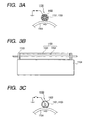
- Figs. 3A and 3B are respectively a schematic top view and a schematic side view of a charging member and a member to be charged in an embodiment of the contact charging device.
- Figs. 3A and 3B also show a contact charging member 1100, a magnetic blush layer 1101 consisting of charge carrier in the contact charging member, a multi-pole magnetic member 1102 of the contact charging member, a spacer 1103 for defining a gap between the contact charging member and the photosensitive member, and a member to be charged (image bearing member) 1104 such as the photosensitive member.
- Fig. 3A shows a state in which the DC bias is applied to the contact charging member 1100, i.e., a DC bias ON state.
- Arrows in the multi-pole magnetic member 1102 in Fig. 3A indicate an example of the magnetic force.
- Fig. 3C shows a state in which the DC bias is not applied to the contact charging member 1100, i.e., a DC bias OFF state.
- the multi-pole magnetic member 1102 of the contact charging member is composed of a magnetic member capable of having a multi-pole structure, for example a metallic or plastic magnet such as a ferrite magnet. Its magnetic flux density is variable depending on various factors such as the process speed, the electric field caused by the potential difference between the applied voltage and the non-charged portion, the dielectric constant of the member to be charged and the surface characteristics, but is preferably at least 500 Gauss, more preferably at least 1000 Gauss, measured at the position of the magnetic pole apart by 1 mm from the surface of the multi-pole magnetic member 1102.
- the shortest distance between the photosensitive member and the multi-pole magnetic member 1102 has to be stably maintained at a constant value by suitable means such as a roller or a spacer 1103, in order to stably control the contact width (hereinafter referred to as "nip width") of the magnetic brush layer 1101.
- This distance is preferably within a range of 50 to 2000 ⁇ m, more preferably 100 to 1000 ⁇ m.
- a mechanism such as a blade for adjusting the nip.
- the magnetic brush layer 1101 of the contact charging member 1100 can be generally composed of magnetic powder such as of ferrite or magnetite, or the carrier of a known magnetic toner.
- the particle size of the magnetic powder is generally within a range of 1 to 100 ⁇ m, preferably not larger than 50 ⁇ m.
- the charge carriers of different particle sizes within the above-mentioned range may be used as a mixture.
- the charge carriers may transfer to the photosensitive member, for example by a mechanical force such as frictional force caused by the rotation of the photosensitive member or an electrical attractive force resulting from an electric field caused by the potential difference between the magnetic brush layer and the non-charged portion of the surface of the photosensitive member, and a part of the charge carriers may be magnetically attracted to the sleeve (developing sleeve) of the developing unit.
- a mechanical force such as frictional force caused by the rotation of the photosensitive member or an electrical attractive force resulting from an electric field caused by the potential difference between the magnetic brush layer and the non-charged portion of the surface of the photosensitive member
- a part of the charge carriers may be magnetically attracted to the sleeve (developing sleeve) of the developing unit.
- This problem can be prevented, as disclosed in JP-A-09-120193 , by setting the distance between the circumferentially adjacent magnetic poles on the surface of the multi-pole magnetic member 1102 smaller than the circumferential width of the nip, whereby at least one magnetic pole can be present within the nip to increase within the nip the force which attracts the magnetic powder toward the multi-pole magnetic member side, thereby preventing the transfer of the magnetic powder toward the member to be charged by the electric field induced between the charging member and the member to be charged.
- the electrophotographic apparatus employing corona charging that is outside the sope of claim 1
- products resulting from ozone are deposited on the surface of the photosensitive member to result in a faint image particularly under a high humidity condition.
- a photosensitive member with the relatively easily abraded surface such as an organic photoconductor (OPC)
- OPC organic photoconductor
- the ozone products formed on the surface can be easily removed for example with polishing means or the like , but an excessive polishing lowers the function of the photosensitive member and reduces the use life thereof.
- the surface insulating layer such as of the amorphous silicon photosensitive member or the CdS photosensitive member employed in the NP process is very hard so that the ozone oxides formed on the surface are difficult to remove by polishing.
- This heating of the photosensitive member is executed for various purposes, but it is executed principally for preventing and eliminating the faint image appearing under a high humidity condition.
- the heating is intended to eliminate the moisture because the surface of the photosensitive member is chemically modified by ozone generated in the corona charger to form hydrophilic radicals (-OH, etc.) to cause moisture absorption, thereby inducing electrophotographically fatal phenomena such as lateral shift of the surface potential. Because NO x , etc. generated by ozone are deposited on the surface of the photosensitive member and absorb moisture, the heating is also executed for the main purpose of removing the moisture.
- the heating is principally achieved by an electric heater provided inside the photosensitive member, though hot air blowing thereto can also be used.
- an electric heater provided inside the photosensitive member
- hot air blowing thereto can also be used.
- a method of temperature control by a rod-shaped heater arranged in the rotary shaft supporting the photosensitive member but there is frequently employed, particularly in the a-Si photosensitive member, a method of arranging a plane-shaped heater on the internal periphery of the photosensitive member, in order to improve the precision of temperature control of the surface of the photosensitive member and to avoid unevenness in the temperature on the entire surface of the photosensitive member.
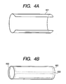
- Fig. 4A is a schematic perspective view showing a plane-shaped heater 601 in a bent state prior to mounting on the photosensitive member
- Fig. 4B is a schematic perspective view showing a state in which the plane-shaped heater 601 is mounted, with a gap 603, on the interior of the photosensitive drum.
- the heater for the photosensitive member there are generally a rod-type heater (not shown in the drawings) not contacting the internal periphery of the photosensitive member and a plane-shaped heater contacting the internal periphery of the photosensitive member, but the latter shows a higher precision of temperature control.
- Figs. 5 and 6 are block diagrams of the generally employed temperature control.
- Fig. 5 shows a heater 401 for the photosensitive member, an AC power source 402, a temperature feedback thermistor 403, and a control circuit 404 for on-off switching or switching in several stages of the power supply to the heater corresponding to the resistance of the thermistor 403.
- Waved lines in Fig. 5 indicate the boundary between the main body of the electrophotographic apparatus and the photosensitive member unit, both being in mutual contact for example by slip rings. Since the thermistor 403 shows a lower resistance at a higher temperature, the temperature of the thermistor is fed back to the control circuit, thereby achieving temperature control.
- Fig. 6 shows a heater 501 for the photosensitive member, an AC power source 502, and a temperature controlling thermoswitch 503. Waved lines in Fig. 6 indicate the boundary between the main body of the electrophotographic apparatus and the photosensitive member unit, both being in mutual contact for example by slip rings. Since the thermoswitch 503 is connected so as to be turned off at a high temperature, thereby achieving temperature control. The turn-off temperature of the thermoswitch is specific thereto.
- the thermistor control shown in Fig. 5 has a higher precision of temperature control.
- the a-Si photosensitive member shows a temperature dependence of the potential as large as 1 to 6 V/°C in the dark potential (300 to 500 V) and 1 to 3 V/°C in the light potential (50 to 200 V), there is often required a precision of ⁇ 1°C in the temperature control and the configuration shown in Fig. 5 is preferred for this case.
- the above precision of the temperature control is achieved in the photosensitive member alone or in a static state where the photosensitive member is still in the electrophotographic apparatus.
- the temperature of the photosensitive member is significantly affected by the room temperature and the copying mode in a dynamic state, i.e., in the actual use state of the photosensitive member involving the paper passing in the electrophotographic apparatus. More specifically, the amount of heat carried away by the paper from the photosensitive member is dependent on the paper temperature, which is affected by the room temperature and by the copying mode (namely whether the copying paper is newly fed from the exterior of the electrophotographic apparatus or fed after passing the fixing unit as in the case of double-side copying or multiple copying).
- the amount of heat carried away by the paper from the photosensitive member is also dependent on the frequency of contact between the paper and the photosensitive member, so that the influence of copying mode (single- or double-side copying, number of copying sheets, paper size (dimension/thickness), etc.). Consequently, in order to maintain the photosensitive member at a constant temperature in the dynamic state, it is necessary to supply the heater with an electric power far larger than that required for reaching the temperature equilibrium, thereby improving the response.
- the first reason is based on the following problem in the shape of the heater.
- a plane-shaped heater is bent and adhered to the internal periphery of the cylindrical photosensitive member, a portion of the photosensitive member corresponding to the seam of this heater shows inferior temperature response, thereby resulting in a temperature difference from the heater.
- a seamless heater for solving the problem, there may be employed a seamless heater.
- the second reason is based on the following problem in the control system.
- the switching control system by a circuit employing a thermistor has various problems depending on the temperature detecting position and the employed control circuit and generally tends to increase the overshooting and the ripple in the temperature control when an electric power increases.
- a PTC heater positive resistance temperature coefficient heater or self-temperature-controlling heater having a temperature dependence in the resistance itself of the heater and showing a higher resistance at a higher temperature is used to be able to maintain the resistor at a constant temperature. Therefore, it is unnecessary to use the temperature control circuit, and there is in principle free from the overshoot and ripple phenomena.
- the PTC heater is self-controlled at an appropriate temperature by the PTC characteristics of the PTC resistor between the electrodes, and is known in a plane-shaped heater formed by integrating a heater layer and electrodes with a film-shaped insulating layer via heat adhesive resin by lamination or by adhesion under heat and pressure.
- a plane-shaped heater formed by integrating a heater layer and electrodes with a film-shaped insulating layer via heat adhesive resin by lamination or by adhesion under heat and pressure.
- the PTC heater employing a pair of electrodes as disclosed in JP-B-57-43996 and JP-B-55-40161 , and other configurations according to various needs such as for a high temperature or a high electric power, but the basic configuration is the same in all PTC heaters.
- the use of a photoconductive layer with a thickness not smaller than 5 ⁇ m and not larger than 15 ⁇ m allows to sufficiently suppress the stress in the deposited a-Si(H, X) film to decrease the peeling of the deposited a-Si(H, X) film to a practically acceptable level or to completely no film peeling level, and the thickness of the drum-shaped metal substrate is set to be not smaller than 1,5 mm and not larger than 2,0 mm, thereby significantly reducing the manufacturing cost thereof.
- a charging device capable of bringing a charging member into contact with the surface of the photosensitive member and applying a voltage to the charging member to charge the photosensitive member exhibits the substantially same potential as that in the conventionally employed photosensitive member with a film thickness of 20 ⁇ m or more. Therefore, it is possible to obtain practically sufficient electrophotographic characteristics, and the disadvantages caused by reducing the thickness of the photoconductive layer can be reduced to a practically acceptable level or completely eliminated.
- the external diameter of the drum-shaped metal substrate is preferably set within a range of 20 mm to 60 mm in consideration of the mechanical strength thereof.
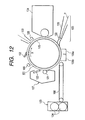
- Fig. 12 is a schematic view showing an example of the image forming apparatus.
- an electrophotographic photosensitive member (hereinafter simply referred to as "photosensitive member") 101 rotated in a direction of an arrow X, there are successively arranged clockwise a contact charger 102, an electrostatic latent image forming position 103, a developing unit 104, a transfer paper supply system 105, a transfer charger 106a, a separation charger 106b, a cleaner 107, a conveying system 108 and a charge eliminating light source 109.
- the photosensitive member 101 may be temperature controlled by a plane-shaped internal heater 125.
- the surface of the photosensitive member 101 is uniformly charged by the contact charger 102 and is subjected to imagewise exposure in the electrostatic latent image forming position 103 to form an electrostatic latent image thereon.
- the electrostatic latent image is rendered visible as a toner image by a developing sleeve which is coated with developer (toner) of the developing unit 104.
- the toner image formed on the photosensitive member 101 is transferred by the transfer charger 106a to a transfer material (paper) P which is supplied by the transfer paper supply system 105 with guiding by a transfer paper guide 119 thereof and top end adjustment by registration rollers 122.
- the transfer material P is then separated from the photosensitive member 101 by the separation charger 106b and/or separation means such as a separation nail (not shown in the drawings), then transported by the conveying system 108, subjected to the fixation of the toner image on the surface by fixing rollers 124 in the fixing unit 123 and discharged from the image forming apparatus.
- the remaining toner, paper dusts, etc. on the surface of the photosensitive member 101 after the toner image transfer are eliminated by a cleaning blade 120 and a cleaning roller (or brush) 121 in the cleaning unit 107, and the cleaned surface is used for the next image formation.
- Photosensitive drums were produced with the apparatus for producing the electrophotographic photoconductive member, shown in Fig. 2 , and with the aforementioned glow discharge decomposition method, by depositing, on aluminum conductive substrates of different thicknesses within a range of 0.5 mm to 5.0 mm, a deposited a-Si:H film under the following conditions so as to obtain a photoconductive layer with a thickness of 3, 5, 15, 20, 35 or 50 ⁇ m.
- Drum-shaped substrate temperature 250°C
- Internal pressure of deposition chamber during formation of deposited film 3.99 Pa (0.03 Torr)
- Discharge frequency 13.56 MHz
- Deposited film-forming rate 20 ⁇ /sec Discharge power: 0.18 W/cm 2
- the difference between the most protruding portion and the most recessed portion was close to 100 ⁇ m, while the difference was not more than 30 pm in the photosensitive drum comprising the conductive substrate of 1.5 mm or 2.0 mm in thickness and the photoconductive layer of 5 ⁇ m or 15 ⁇ m in thickness.
- the difference was about 30 ⁇ m, while the difference was about 10 ⁇ m to about 20 ⁇ m in the photosensitive drum comprising the conductive substrate of 2.5 mm or 3.0 mm in thickness and the photoconductive layer of 5 ⁇ m or 15 ⁇ m in thickness. Also in the photosensitive drum comprising the conductive substrate of 3.5 mm or 5.0 mm in thickness, the difference was not more than a range of 10 ⁇ m to 20 ⁇ m or less in any thickness of the photoconductive layer. The details of this evaluation are shown in Table 3.
- Photosensitive drums were produced under the same conditions as in Example 1, and the obtained images were evaluated for the fogging under the same conditions as in Example 1, except that the charger was replaced by a corona charger.
- the obtained results are shown in Table 4.
- the results were scarcely dependent on the thickness of the conductive substrate but was dependent on the thickness of the photoconductive layer.
- the drum comprising the photoconductive layer of 3, 5 or 15 ⁇ m in thickness showed severely fogging and could not provide satisfactory images because a sufficient contrast in potential could not be secured.
- Photosensitive members comprising the conductive substrate with a different thickness and the photoconductive layer with a different thickness were produced by using a PTC heater of flexible seamless cylindrical shape as shown in Fig. 7B , adhered to the internal periphery of the photosensitive member, and by using no temperature control circuit.
- the photosensitive member was set on an experimental equipment, and an optimum power corresponding to the heat capacity of the photosensitive member was supplied to the heater.
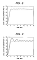
- the temperature variation of the surface of the photosensitive member (drum) was measured with the lapse of time from the starting of supplying the power in a static state in which the temperature of the photosensitive member was controlled so as to reach 45°C. The obtained results are shown in Fig. 8 and Table 5.
- the photosensitive members comprising the conductive substrate of 0.05 mm in thickness showed film peeling at the film deposition or at the measurement because of the insufficient strength of the conductive substrate, so that the measurement was possible only up to a film thickness of 5 ⁇ m.
- Figs. 7A and 7B respectively show the shapes of the heater for the photosensitive member prior to and after mounting on the photosensitive member. Mounting or detachment of the heater is executed by partially deforming the heater as shown in Fig. 7A , thereby reducing the external diameter. Upon mounting in the photosensitive member, the heater returns to the cylindrical shape, thereby adhering to the internal periphery of the photosensitive member and has an external diameter equal to the internal diameter of the photosensitive member.
- Fig. 8 shows a representative example of the actual measurements, and the a substantially same tendency was obtained in all the measuring points on the photosensitive member. Even in the case of high-speed heating with a large electric power, there was not observed the temperature difference depending on the measuring position at the switching operation and the temperature variation with the lapse of time in the same measuring position (ripple in temperature control).
- Photosensitive members comprising the conductive substrate with a different thickness and the photoconductive layer with a different thickness were produced by using a temperature control circuit as shown in Fig. 5 and a conventional seamed heater of plane shape rounded and adhered to the internal periphery of the photosensitive member as shown in Figs. 4A and 4B or a conventional seamless, cylindrical, flexible heater adhered to the internal periphery of the photosensitive member.
- the photosensitive member was set on an experimental equipment, and the power used in Example 2 corresponding to the heat capacity of the photosensitive member was supplied to the heater.
- the temperature variation of the surface of the photosensitive member was measured with the lapse of time from the starting of supplying the power in a static state in which the temperature of the photosensitive member was controlled so as to reach 45°C.
- the obtained results are shown in Fig. 9 and Table 6.
- the photosensitive members comprising the conductive substrate of 0.05 mm in thickness showed film peeling at the film deposition or at the measurement because of the insufficient strength of the conductive substrate, so that the measurement was possible only up to a film thickness of the photoconductive layer of 5 ⁇ m.
- the seamed heater showed a large temperature difference at the switching operation, between the seam portion indicated by a broken line in Fig. 9 and the seamless portion indicated by a solid line in Fig. 9 .
- the seamless heater all the measuring points showed similar results as indicated by a solid line in Fig. 9 , so that the temperature difference between the measuring positions was not observed at the switching operation but the temperature variation with the lapse of time in the same measuring position (ripple in temperature control) was observed.
- Photosensitive members comprising the conductive substrate with a different thickness and the photoconductive layer with a different thickness were produced by using a PTC heater of a flexible seamless cylindrical shape as shown in Fig. 7B and adhered to the internal periphery of the photosensitive member and by using no temperature control circuit.
- the photosensitive member was set on an experimental equipment, and an optimum power corresponding to the heat capacity of the photosensitive member was supplied to the heater and was controlled so that the temperature of the photosensitive member reached 45°C.
- the variation of the surface temperature of the photosensitive member (drum) was measured with the lapse of time while papers were passed continuously in an environmental temperature of 15°C. The obtained results are shown in Fig. 10 and Table 7.
- the photosensitive members comprising the conductive substrate of 0.05 mm in thickness showed film peeling at the film deposition or at the measurement because of the insufficient strength of the conductive substrate, so that the measurement was possible only up to a film thickness of the conductive substrate of 5 ⁇ m.
- Fig. 10 shows a representative example of the actual measurements. As shown in Table 7, there was scarcely observed the dependency of the thickness of the photoconductive layer on the temperature variation, and satisfactory results were obtained in all the cases when the optimum electric power corresponding to the heat capacity of the photosensitive member was employed. Particularly, more satisfactory results were obtained in the case of a larger thickness of the conductive substrate, because of the larger heat capacity.
- the above constitution eliminated the temperature variation with the lapse of time (ripple in temperature control) even in the dynamic state, thereby eliminating the unevenness in the potential due to the aforementioned temperature characteristics to prevent the small unevenness of the image density conventionally generated in the continuous paper feeding.
- the elimination of uneven potential eliminates the conventional potential control fluctuation due to the uneven potential resulting from the temperature characteristics, i.e., control potential variation, thereby improving the convergency of potential and the stability of the image density.
- Photosensitive members comprising the conductive substrate with a different thickness and the photoconductive layer with a different thickness were produced by using a temperature control circuit as shown in Fig. 5 and a seamless cylindrical flexible heater adhered to the internal periphery of the photosensitive member.
- the photosensitive member was set on an experimental equipment, and the power used in Example 3 corresponding to the heat capacity of the photosensitive member was supplied to the heater and was controlled so that the photosensitive member reached 45°C.
- the temperature variation of the surface of the photosensitive member (drum) was measured with the lapse of time while papers were passed continuously in an environmental temperature of 15°C. The obtained results are shown in Fig. 11 and Table 8.
- the photosensitive members comprising the substrate of 0.05 mm in thickness showed film peeling at the film deposition or at the measurement because of the insufficient strength of the conductive substrate, so that the measurement was possible only up to the photoconductive layer thickness of 5 ⁇ m.
- the thickness of the photoconductive layer is set to be not smaller than 5 ⁇ m and not larger than 15 ⁇ m to be able to sufficiently suppress the stress in the deposited a-Si(H, X) film, thereby maintaining the peeling thereof at a practically acceptable level or at no film peeling level.
- the thickness of the drum-shaped metal substrate is set to be not smaller than 1,5 mm and not larger than 2,0 mm, whereby the producing cost can be significantly reduced.
- the charging device there is employed a contact charging device for contacting a charging member with the surface of the photosensitive member and applying a voltage to the charging member to charge the photosensitive member, thereby being able to obtain the potential of a level substantially equal to that in the conventionally used photosensitive member comprising the photoconductive layer with a film thickness of 20 ⁇ m or more. It is therefore rendered possible to obtain practically sufficient electrophotographic characteristics and to suppress the disadvantages generated by making a photoconductive layer thinner to a practically acceptable level or to completely eliminate the disadvantages.
- the use of a PTC heater with seamless structure makes it possible to supply an electric power far larger than that required for reaching the temperature equilibrium, thereby improving the response and enabling high-speed heating, and to execute the temperature control without overshoot and ripple phenomena even in the dynamic state involving the paper feeding.
Landscapes
- Physics & Mathematics (AREA)
- General Physics & Mathematics (AREA)
- Chemical & Material Sciences (AREA)
- Inorganic Chemistry (AREA)
- Photoreceptors In Electrophotography (AREA)
- Electrostatic Charge, Transfer And Separation In Electrography (AREA)
Claims (5)
- Bilderzeugungsgerät mit einem elektrophotografischen, lichtempfindlichen Bauteil (101), das eine zylindrische Form aufweist, wobei das elektrophotografische, lichtempfindliche Bauteil (101) Folgendes aufweist:ein leitfähiges Substrat mit einer Dicke, die nicht kleiner als 1,5 mm und nicht größer als 2,0 mm ist; undeine Licht empfangende Schicht mit einer photoleitfähigen Schicht auf dem leitfähigen Substrat, wobei die Licht empfangende Schicht zumindest amorphes Silizium beinhaltet, wobei die photoleitfähige Schicht eine Dicke aufweist, die nicht kleiner als 5 µm und nicht größer als 15 µm ist, und wobei eine Differenz zwischen einem höchsten Abschnitt und einem tiefsten Abschnitt des lichtempfindlichen Bauteils (101) nicht mehr als 30 µm ist;wobei das Bilderzeugungsgerät des Weiteren eine Aufladevorrichtung zum Aufladen des lichtempfindlichen Bauteils (101) aufweist, wobei die Aufladevorrichtung eine Vorrichtung zum Berühren eines zylindrischen Aufladebauteils (1100) mit einer Fläche des lichtempfindlichen Bauteils (101) und zum Anlegen einer Spannung an das zylindrische Aufladebauteil (101) ist, um das lichtempfindliche Bauteil (101) aufzuladen.
- Bilderzeugungsgerät nach Anspruch 1, wobei das leitfähige Substrat eine zylindrische Form aufweist, wobei eine Heizvorrichtung (125) an einem Innenumfang des leitenden Substrats angefügt ist, und die Heizvorrichtung (125) eine flexible, übergangslose, zylindrische Form aufweist und einen positiven Temperaturkoeffizienten aufweist.
- Bilderzeugungsgerät nach Anspruch 1 oder 2, wobei das leitfähige Substrat aus Aluminium oder einer Aluminiumlegierung gebildet ist.
- Bilderzeugungsgerät nach einem der Ansprüche 1 bis 3, wobei das leitfähige Substrat einen Außendurchmesser von 20 mm bis 60 mm aufweist.
- Bilderzeugungsgerät nach einem der Ansprüche 1 bis 4, wobei eine Temperaturabhängigkeit des Potentials des lichtempfindlichen Bauteils (101) zwischen 1 und 6 V/°C bei einem Dunkelpotential von 300 V bis 500 V und zwischen 1 und 3 V/°C bei einem Hellpotential von 50 V bis 200 V beträgt.
Priority Applications (1)
| Application Number | Priority Date | Filing Date | Title |
|---|---|---|---|
| EP04006392A EP1429193A3 (de) | 1998-05-14 | 1999-05-12 | Bildformender Apparat |
Applications Claiming Priority (4)
| Application Number | Priority Date | Filing Date | Title |
|---|---|---|---|
| JP13224598 | 1998-05-14 | ||
| JP13224598A JPH11327183A (ja) | 1998-05-14 | 1998-05-14 | 電子写真感光体及び電子写真装置 |
| JP13390098 | 1998-05-15 | ||
| JP13390098A JPH11327258A (ja) | 1998-05-15 | 1998-05-15 | 電子写真装置 |
Related Child Applications (1)
| Application Number | Title | Priority Date | Filing Date |
|---|---|---|---|
| EP04006392A Division EP1429193A3 (de) | 1998-05-14 | 1999-05-12 | Bildformender Apparat |
Publications (2)
| Publication Number | Publication Date |
|---|---|
| EP0957405A1 EP0957405A1 (de) | 1999-11-17 |
| EP0957405B1 true EP0957405B1 (de) | 2009-10-21 |
Family
ID=26466870
Family Applications (2)
| Application Number | Title | Priority Date | Filing Date |
|---|---|---|---|
| EP99109499A Expired - Lifetime EP0957405B1 (de) | 1998-05-14 | 1999-05-12 | Bildherstellungsapparat |
| EP04006392A Withdrawn EP1429193A3 (de) | 1998-05-14 | 1999-05-12 | Bildformender Apparat |
Family Applications After (1)
| Application Number | Title | Priority Date | Filing Date |
|---|---|---|---|
| EP04006392A Withdrawn EP1429193A3 (de) | 1998-05-14 | 1999-05-12 | Bildformender Apparat |
Country Status (3)
| Country | Link |
|---|---|
| US (1) | US6122467A (de) |
| EP (2) | EP0957405B1 (de) |
| DE (1) | DE69941551D1 (de) |
Families Citing this family (11)
| Publication number | Priority date | Publication date | Assignee | Title |
|---|---|---|---|---|
| US6904243B2 (en) | 2002-06-07 | 2005-06-07 | Hewlett-Packard Development Company, L.P. | Image forming system and method and photoconductor having wear indicator |
| JP4242901B2 (ja) * | 2006-02-24 | 2009-03-25 | 京セラ株式会社 | 画像形成装置 |
| JP4377923B2 (ja) * | 2006-02-24 | 2009-12-02 | 京セラ株式会社 | 画像形成装置 |
| JP5121785B2 (ja) | 2008-07-25 | 2013-01-16 | キヤノン株式会社 | 電子写真感光体および電子写真装置 |
| JP5653186B2 (ja) * | 2009-11-25 | 2015-01-14 | キヤノン株式会社 | 電子写真装置 |
| JP5675287B2 (ja) * | 2009-11-26 | 2015-02-25 | キヤノン株式会社 | 電子写真感光体および電子写真装置 |
| JP5675292B2 (ja) * | 2009-11-27 | 2015-02-25 | キヤノン株式会社 | 電子写真感光体および電子写真装置 |
| JP5777419B2 (ja) | 2010-06-28 | 2015-09-09 | キヤノン株式会社 | 電子写真感光体および電子写真装置 |
| JP5954040B2 (ja) | 2012-08-10 | 2016-07-20 | 富士ゼロックス株式会社 | 電子写真感光体、プロセスカートリッジ、及び画像形成装置 |
| EP4097542A4 (de) * | 2020-03-26 | 2023-11-01 | Hewlett-Packard Development Company, L.P. | Heizung für eine drucktrommel |
| JP2025044750A (ja) * | 2023-09-20 | 2025-04-02 | 富士フイルムビジネスイノベーション株式会社 | 画像形成装置 |
Family Cites Families (22)
| Publication number | Priority date | Publication date | Assignee | Title |
|---|---|---|---|---|
| JPS5331242A (en) * | 1976-09-02 | 1978-03-24 | Matsushita Electric Ind Co Ltd | High frequency wave heating device |
| DE2746967C2 (de) * | 1977-10-19 | 1981-09-24 | Siemens AG, 1000 Berlin und 8000 München | Elektrofotographische Aufzeichnungstrommel |
| GB2102028B (en) * | 1977-12-22 | 1983-06-08 | Canon Kk | Electrophotographic photosensitive member and process for production thereof |
| AU530905B2 (en) * | 1977-12-22 | 1983-08-04 | Canon Kabushiki Kaisha | Electrophotographic photosensitive member |
| JPS5540161A (en) * | 1978-09-13 | 1980-03-21 | Mitsubishi Electric Corp | Derailing detector for elevator |
| US4461820A (en) * | 1981-02-06 | 1984-07-24 | Canon Kabushiki Kaisha | Amorphous silicon electrophotographic image-forming member having an aluminum oxide coated substrate |
| DE3481225D1 (de) * | 1983-09-30 | 1990-03-08 | Mita Industrial Co Ltd | Elektrophotographische einrichtung, eine lichtempfindliche schicht von amorphem silizium-lichtleiter enthaltend. |
| JP2519414B2 (ja) * | 1986-01-30 | 1996-07-31 | 三田工業株式会社 | 電子写真装置 |
| JPS6391664A (ja) * | 1986-10-06 | 1988-04-22 | Canon Inc | 光受容部材 |
| JPS63121851A (ja) * | 1986-11-11 | 1988-05-25 | Canon Inc | 電子写真用光受容部材 |
| JPS63210864A (ja) * | 1987-02-27 | 1988-09-01 | Canon Inc | 画像形成装置 |
| JPH01238677A (ja) * | 1988-03-19 | 1989-09-22 | Ricoh Co Ltd | 電子写真プロセス |
| JP2829629B2 (ja) * | 1988-07-01 | 1998-11-25 | キヤノン株式会社 | アモルファスシリコン系感光体を用いた電子写真法による画像形成方法及び電子写真装置 |
| JPH02251866A (ja) * | 1989-03-24 | 1990-10-09 | Hitachi Koki Co Ltd | アモルファスシリコン感光体の接触帯電方法 |
| US5392098A (en) * | 1991-05-30 | 1995-02-21 | Canon Kabushiki Kaisha | Electrophotographic apparatus with amorphous silicon-carbon photosensitive member driven relative to light source |
| US5191381A (en) * | 1991-08-12 | 1993-03-02 | Jie Yuan | PTC ceramic heat roller for fixing toner image |
| US5592274A (en) * | 1992-01-31 | 1997-01-07 | Fuji Xerox Co., Ltd. | Electrophotographic apparatus and process for simultaneously transferring and fixing toner image onto transfer paper |
| US5729800A (en) * | 1993-10-29 | 1998-03-17 | Kyocera Corporation | Electrophotographic apparatus having an a-Si photosensitive drum assembled therein |
| JP3606395B2 (ja) * | 1994-04-27 | 2005-01-05 | キヤノン株式会社 | 電子写真用光受容部材 |
| DE69525996T2 (de) * | 1994-06-22 | 2002-09-19 | Canon K.K., Tokio/Tokyo | Elektrophotographisches Gerät |
| JP3247283B2 (ja) * | 1995-10-25 | 2002-01-15 | キヤノン株式会社 | 帯電装置及び画像形成装置 |
| JP3618919B2 (ja) * | 1996-08-23 | 2005-02-09 | キヤノン株式会社 | 電子写真用光受容部材とその形成方法 |
-
1999
- 1999-05-12 EP EP99109499A patent/EP0957405B1/de not_active Expired - Lifetime
- 1999-05-12 DE DE69941551T patent/DE69941551D1/de not_active Expired - Lifetime
- 1999-05-12 EP EP04006392A patent/EP1429193A3/de not_active Withdrawn
- 1999-05-13 US US09/310,986 patent/US6122467A/en not_active Expired - Lifetime
Also Published As
| Publication number | Publication date |
|---|---|
| EP1429193A3 (de) | 2004-07-07 |
| EP1429193A2 (de) | 2004-06-16 |
| EP0957405A1 (de) | 1999-11-17 |
| US6122467A (en) | 2000-09-19 |
| DE69941551D1 (de) | 2009-12-03 |
Similar Documents
| Publication | Publication Date | Title |
|---|---|---|
| EP0957405B1 (de) | Bildherstellungsapparat | |
| EP0957404B1 (de) | Elektrophotographischer Bildherstellungsapparat | |
| JP4377923B2 (ja) | 画像形成装置 | |
| JPH08160821A (ja) | 電子写真装置 | |
| EP0989470B1 (de) | Bilderzeugungsgerät | |
| EP0762229B1 (de) | Bilderzeugungsgerät und Bilderzeugungsverfahren | |
| EP0987603B1 (de) | Elektrophotographisches photoempfindliches Element und elektrophotographisches Gerät | |
| JP2004077650A (ja) | 電子写真装置 | |
| US6240269B1 (en) | Image forming apparatus having a photosensitive member of amorphous silicon base and system for exposing and charging the photosensitive member | |
| JP3548327B2 (ja) | 電子写真用光受容部材 | |
| US20100260517A1 (en) | Electrophotographic Photosensitive Body and Image Forming Device Having an Electrophotographic Photosensitive Body | |
| JPH11327258A (ja) | 電子写真装置 | |
| JPH11327183A (ja) | 電子写真感光体及び電子写真装置 | |
| JP2001330978A (ja) | 電子写真感光体及び電子写真装置 | |
| JP3535664B2 (ja) | 電子写真装置 | |
| JP5311830B2 (ja) | 電子写真装置 | |
| JPH08171337A (ja) | 電子写真装置の除湿装置 | |
| JP2011221107A (ja) | 画像形成装置 | |
| JP4416621B2 (ja) | 電子写真感光体の表面の研磨方法および電子写真感光体の製造方法 | |
| JP2002082463A (ja) | 電子写真感光体および電子写真装置 | |
| JP3943713B2 (ja) | 電子写真感光体及び電子写真装置 | |
| JPH08227260A (ja) | 電子写真装置の除湿装置 | |
| JP2003107848A (ja) | 磁気ブラシ帯電装置 | |
| JP2002372837A (ja) | 磁気ブラシ帯電装置 | |
| JP2004077651A (ja) | 電子写真装置 |
Legal Events
| Date | Code | Title | Description |
|---|---|---|---|
| PUAI | Public reference made under article 153(3) epc to a published international application that has entered the european phase |
Free format text: ORIGINAL CODE: 0009012 |
|
| AK | Designated contracting states |
Kind code of ref document: A1 Designated state(s): DE FR GB IT |
|
| AX | Request for extension of the european patent |
Free format text: AL;LT;LV;MK;RO;SI |
|
| 17P | Request for examination filed |
Effective date: 20000428 |
|
| AKX | Designation fees paid |
Free format text: DE FR GB IT |
|
| 17Q | First examination report despatched |
Effective date: 20031031 |
|
| GRAP | Despatch of communication of intention to grant a patent |
Free format text: ORIGINAL CODE: EPIDOSNIGR1 |
|
| RIN1 | Information on inventor provided before grant (corrected) |
Inventor name: OWAKI, HIRONORI, C/O CANON KABUSHIKI KAISHA Inventor name: KAWADA, MASAYA, C/O CANON KABUSHIKI KAISHA Inventor name: NAKAYAMA, YUJI, C/O CANON KABUSHIKI KAISHA Inventor name: EHARA, TOSHIYUKI, C/O CANON KABUSHIKI KAISHA |
|
| GRAS | Grant fee paid |
Free format text: ORIGINAL CODE: EPIDOSNIGR3 |
|
| GRAA | (expected) grant |
Free format text: ORIGINAL CODE: 0009210 |
|
| AK | Designated contracting states |
Kind code of ref document: B1 Designated state(s): DE FR GB IT |
|
| REG | Reference to a national code |
Ref country code: GB Ref legal event code: FG4D |
|
| REF | Corresponds to: |
Ref document number: 69941551 Country of ref document: DE Date of ref document: 20091203 Kind code of ref document: P |
|
| PLBE | No opposition filed within time limit |
Free format text: ORIGINAL CODE: 0009261 |
|
| STAA | Information on the status of an ep patent application or granted ep patent |
Free format text: STATUS: NO OPPOSITION FILED WITHIN TIME LIMIT |
|
| 26N | No opposition filed |
Effective date: 20100722 |
|
| REG | Reference to a national code |
Ref country code: FR Ref legal event code: PLFP Year of fee payment: 17 |
|
| PGFP | Annual fee paid to national office [announced via postgrant information from national office to epo] |
Ref country code: GB Payment date: 20150528 Year of fee payment: 17 Ref country code: DE Payment date: 20150531 Year of fee payment: 17 |
|
| PGFP | Annual fee paid to national office [announced via postgrant information from national office to epo] |
Ref country code: IT Payment date: 20150522 Year of fee payment: 17 Ref country code: FR Payment date: 20150527 Year of fee payment: 17 |
|
| REG | Reference to a national code |
Ref country code: DE Ref legal event code: R119 Ref document number: 69941551 Country of ref document: DE |
|
| GBPC | Gb: european patent ceased through non-payment of renewal fee |
Effective date: 20160512 |
|
| PG25 | Lapsed in a contracting state [announced via postgrant information from national office to epo] |
Ref country code: IT Free format text: LAPSE BECAUSE OF NON-PAYMENT OF DUE FEES Effective date: 20160512 |
|
| REG | Reference to a national code |
Ref country code: FR Ref legal event code: ST Effective date: 20170131 |
|
| PG25 | Lapsed in a contracting state [announced via postgrant information from national office to epo] |
Ref country code: DE Free format text: LAPSE BECAUSE OF NON-PAYMENT OF DUE FEES Effective date: 20161201 Ref country code: FR Free format text: LAPSE BECAUSE OF NON-PAYMENT OF DUE FEES Effective date: 20160531 |
|
| PG25 | Lapsed in a contracting state [announced via postgrant information from national office to epo] |
Ref country code: GB Free format text: LAPSE BECAUSE OF NON-PAYMENT OF DUE FEES Effective date: 20160512 |