EP0898309A2 - Überbrückungsgeschützter Anschlussleiterentwurf einer integrierten Schaltung - Google Patents
Überbrückungsgeschützter Anschlussleiterentwurf einer integrierten Schaltung Download PDFInfo
- Publication number
- EP0898309A2 EP0898309A2 EP98306673A EP98306673A EP0898309A2 EP 0898309 A2 EP0898309 A2 EP 0898309A2 EP 98306673 A EP98306673 A EP 98306673A EP 98306673 A EP98306673 A EP 98306673A EP 0898309 A2 EP0898309 A2 EP 0898309A2
- Authority
- EP
- European Patent Office
- Prior art keywords
- leads
- integrated circuit
- lead
- bend
- circuitry
- Prior art date
- Legal status (The legal status is an assumption and is not a legal conclusion. Google has not performed a legal analysis and makes no representation as to the accuracy of the status listed.)
- Withdrawn
Links
Images


Classifications
-
- H—ELECTRICITY
- H05—ELECTRIC TECHNIQUES NOT OTHERWISE PROVIDED FOR
- H05K—PRINTED CIRCUITS; CASINGS OR CONSTRUCTIONAL DETAILS OF ELECTRIC APPARATUS; MANUFACTURE OF ASSEMBLAGES OF ELECTRICAL COMPONENTS
- H05K3/00—Apparatus or processes for manufacturing printed circuits
- H05K3/30—Assembling printed circuits with electric components, e.g. with resistors
- H05K3/32—Assembling printed circuits with electric components, e.g. with resistors electrically connecting electric components or wires to printed circuits
- H05K3/34—Assembling printed circuits with electric components, e.g. with resistors electrically connecting electric components or wires to printed circuits by soldering
- H05K3/341—Surface mounted components
- H05K3/3421—Leaded components
- H05K3/3426—Leaded components characterised by the leads
-
- H—ELECTRICITY
- H10—SEMICONDUCTOR DEVICES; ELECTRIC SOLID-STATE DEVICES NOT OTHERWISE PROVIDED FOR
- H10W—GENERIC PACKAGES, INTERCONNECTIONS, CONNECTORS OR OTHER CONSTRUCTIONAL DETAILS OF DEVICES COVERED BY CLASS H10
- H10W74/00—Encapsulations, e.g. protective coatings
- H10W74/10—Encapsulations, e.g. protective coatings characterised by their shape or disposition
- H10W74/111—Encapsulations, e.g. protective coatings characterised by their shape or disposition the semiconductor body being completely enclosed
- H10W74/121—Encapsulations, e.g. protective coatings characterised by their shape or disposition the semiconductor body being completely enclosed by multiple encapsulations, e.g. by a thin protective coating and a thick encapsulation
-
- Y—GENERAL TAGGING OF NEW TECHNOLOGICAL DEVELOPMENTS; GENERAL TAGGING OF CROSS-SECTIONAL TECHNOLOGIES SPANNING OVER SEVERAL SECTIONS OF THE IPC; TECHNICAL SUBJECTS COVERED BY FORMER USPC CROSS-REFERENCE ART COLLECTIONS [XRACs] AND DIGESTS
- Y02—TECHNOLOGIES OR APPLICATIONS FOR MITIGATION OR ADAPTATION AGAINST CLIMATE CHANGE
- Y02P—CLIMATE CHANGE MITIGATION TECHNOLOGIES IN THE PRODUCTION OR PROCESSING OF GOODS
- Y02P70/00—Climate change mitigation technologies in the production process for final industrial or consumer products
- Y02P70/50—Manufacturing or production processes characterised by the final manufactured product
Definitions
- This invention relates to integrated circuit (IC) packaging.
- IC integrated circuit
- This invention provides an IC package, including resistor networks, design and method of applying the package design so that electrical bridging between metal leads caused by wave soldering operations is reduced.
- U.S. patent no. 5,569,880 is a surface mountable electronic component and method of making the same.
- U.S. patent no. 5,495,669 is a method of making box contacts.
- U.S. patent no. 5,387,486 is a radiation-polymerizable mixture and process for producing a solder resist mask.
- U.S. patent no. 5,210,375 is an electronic device package-carrier assembly ready to be mounted onto a substrate.
- U.S. patent no. 5,147,084 is an interconnection structure and test method.
- U.S. patent no. 5,136,122 is a braided fibre omega connector.
- U.S. patent no. 5,196,268 is an integrated circuit interconnect leads releasably mounted on film.
- U.S. patent no. 5,098,863 is a method of stabilising lead dimensions on high pin count surface mount IC packages.
- U.S. patent no. 5,057,456 is a method of manufacturing a tab semiconductor package by securing a thin insulating frame to inner leads of the package.
- U.S. patent no. 4,289,588 is an apparatus for automated application of heat sensitive tape.
- U.S. patent no.4,204,317 is a method of making a lead frame.
- a common problem occurring during PCB population occurs during wave soldering of the ICs to the PCB.
- ICs are temporarily mounted, via glue, for example, to the PCB.
- the PCB is then positioned upside down and run through a wave solder.
- the wave solder typically will completely submerge the ICs. Any metal surfaces exposed to the solder will be coated with a thin layer of solder.
- solder will pool up on the horizontal regions. The lateral surfaces can collect enough solder to actually form a bridge between adjacent leads, thereby shorting out the circuit and creating a defective PCB. Therefore, there was a need for an IC package that has an anti-bridge design.
- Fig. 1 illustrates one solution for an anti-bridge design.
- the IC 10 has electrical circuitry 12 mounted thereon. Gull wing leads 14, are embedded into the IC body 16, and are coupled to the circuitry 12 via conductors 18 in a known fashion.
- the IC 10 is mounted to a printed circuit board 20, having bond pads 22, and electrical components or traces 24 thereon. Insulating material 30, like epoxy covers at least one side of IC 10 to insulate the circuitry 12 from traces 24. Material 30 is added to prevent bridging between electrical components or traces 24 and circuitry 12 during wave soldering operations. It is noted that the insulating material is applied to the IC body 16 when the leads are in an unbent or straight condition.
- Ultraviolet curable material 40 like polyurethane, is formed in cup region 15 of a gull wing lead design.
- the UV material 40 is added after the leads have been formed into the gull wing design.
- This two step two material covercoat has proved successful in eliminating the bridging of solder 25 in the gull wing cup regions 15 as a result of subsequent wave soldering operations.
- IC integrated circuit
- it provides an IC package design and method of applying the package design to an IC that provides for anti-bridging between metal leads because of PCB wave soldering operations.
- an integrated circuit comprising:
- An additional feature of the invention is to provide an anti-bridge IC package design that extends a typical bottom cover coat out onto the leads sufficient to prevent solder pooling located in cup regions of gull wing shaped leads.
- a further feature of the invention is to provide a method of applying covercoat material to the IC and the leads in the same process step.
- Another feature of the invention is to provide a resilient material wheel and related manufacturing equipment that apply a single material, like ep-
- FIG. 1 is a cross section of a related art IC employing two separate coating materials mounted to a PCB.
- FIG. 2 is a cross section of a preferred IC embodiment employing one coating material mounted to a PCB.
- FIG. S is a cross sectional side view of the leads of the IC illustrating solder bridging and anti-bridging design effects.
- FIG. 4a illustrates an end view of a resilient material wheel employed to apply the cover coating material on the preferred embodiment.
- FIG. 4b illustrates a side view of FIG. 4a.
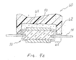
- FIG. 4c illustrates an end view: of a FIG. 4a as material is applied to an IC.
- the present invention provides an integrated circuit anti-bridging leads design.
- FIG. 2 there is a preferred embodiment IC 10 with an anti-bridge design.
- the IC 10 has electrical circuitry 12 mounted thereon.
- Gull wing leads 14, are embedded into IC body 16, which is a ceramic based material, are bent at a first bend 17 and a second bend 19, and are coupled to circuitry 12 via conductors 18 in a known fashion.
- the IC 10 is mounted to a printed circuit board 20, having band pads 22, and electrical components or traces 24 thereon.
- Insulating material 50 like epoxy, forms a covercoat layer that covers at least a bottom side of the IC 10 to insulate the circuitry 12 from POB traces/components 24.
- cover coat 50 is also formed in cup region 15 of gull wing leads 14 to prevent solder bridging typically occurring during subsequent wave soldering operations.
- the cup region 15 extends from the outer surface of IC body 16 to a position beyond the bend 17 in the lead 14.
- Solder layer 25 covers all exposed solderable material, for example leads 14 and bond pads 22.
- FIG 3 there is illustrated a sectional side view of leads 14 extending from body 18 that have been put through a wave soldering operation.
- leads 14 there are two situations illustrated; the left two leads 14 have solder 25 forming a defect causing solder bridge 52.
- the second situation is illustrated by the two right leads 14, showing where bridging is avoided 54 because of the existence of a non-solderable covercoat layer 50 that at least covers the bottom side 58 of the leads.
- wheel 80 for applying cover coat material onto straight leads of an IC.
- wheel 60 has ridges 82, and channel 64 that applies epoxy 50 onto at least the bottom side of the first portion 65 of leads 14 and at least the bottom surface of IC 10.
- the method of assembling an anti-bridge IC and thereby mounting it to a PCB is as follows: An IC body having circuitry and unbent leads mounted thereon is provided. The IC body may have subsequent circuitry 12 applied thereon. The IC is then run under the elastic material wheel 60 to simultaneously cover at least the bottom side of the IC and to also cover at least a bottom face of the first portion 65. Of course, the wheel 60 first is covered with covercoat material prior to coating the IC 10. Wheel 60 will receive ICs 10 so that the leads first portion 65 will be coated by ridge 62, channel 64 will cover the body 16, and the sides of the ridges will cover the sides of the body 16. The covercoat can then be hardened if needed.
- the straight leads are then formed into the gull wing leads illustrated in Figs. 1 and 2.
- the ICs are then ready to be temporarily attach to bond pads 22 on a FOB 20 by gluing or any known method.
- the ROB is then placed upside down through a wave soldering operation, which completely submerges the mounted IC.
- the FOB is then removed from the wave soldering operation, where solder is maintained only on solderable material like the exposed surfaces of the leads and bond pads 22, as shown in FIG. 2.
- cover coat 50 should be extended beyond the first bend 17 in the metal leads to achieve effective anti-bridging protection. Additionally, it is noted that cover coat 50 may cover both the bottom and sides of leads 14 for increased anti-bridging and even the top side thereof. Although, it has been discovered that simply covering the bottom side of leads 14 will suffice.
- the preferred embodiment designs its circuitry 12 and traces 18 using unsolderable thick film material, which is used to make resistor networks which are passive devices.
- a cover coat 50 may be required thereon to prevent solder from forming thereon during wave soldering process steps, for example.
- covercoat material application can be controlled.
- covercoat material may only cover the bottom face 56 if a small amount of covercoat material is applied. It may be possible to additionally cover the side faces if more covercoat material is applied from the wheel. A thick layer of covercoat may even extend between adjacent leads if a large amount is applied, appearing like a solder bridge.
- both sides of leads 14 may be easily coated by using two wheels 60, one wheel on each side of the IC 10. In this fashion, both sides of the IC body 16 can also be covered.
- An additional variation of the invention contemplates the use of applying any type of covercoat material that serves the purpose of 1) insulating IC electronics and 2) creating an anti-bridge on metal leads extending from the IC body.
- a very spongy material may work with gear teeth, which work to separate individual ICs as covercoat material 50 is applied thereto.
- cover coat application tool that is not a wheel, but a stamp pad that is rewetted with covercoat material between stamping, or even spraying covercoat material onto the IC with directed micro spray nozzles.
- the preferred embodiment describes covering the bottom side of the IC 10 and leads 14 with a covercoat material, like epoxy, it is contemplated to cover only a top side of both parts, or any combination of sides thereof, depending upon the application.
- the preferred embodiment describes placing epoxy 50 in the cup region that means extending from the body surface to a point just past the first bend 17. It is even contemplated that the epoxy will extend completely around the first bend and potentially all the way to the second bend 19. Additionally, it is expected that this method and design will work equally as well with other type of lead designs like "J", leads etc.
- circuitry be placed only on the top side, or only on the bottom side.
Landscapes
- Engineering & Computer Science (AREA)
- Manufacturing & Machinery (AREA)
- Microelectronics & Electronic Packaging (AREA)
- Non-Metallic Protective Coatings For Printed Circuits (AREA)
- Lead Frames For Integrated Circuits (AREA)
Applications Claiming Priority (2)
| Application Number | Priority Date | Filing Date | Title |
|---|---|---|---|
| US915268 | 1997-08-20 | ||
| US08/915,268 US5844308A (en) | 1997-08-20 | 1997-08-20 | Integrated circuit anti-bridging leads design |
Publications (2)
| Publication Number | Publication Date |
|---|---|
| EP0898309A2 true EP0898309A2 (de) | 1999-02-24 |
| EP0898309A3 EP0898309A3 (de) | 2000-02-09 |
Family
ID=25435482
Family Applications (1)
| Application Number | Title | Priority Date | Filing Date |
|---|---|---|---|
| EP98306673A Withdrawn EP0898309A3 (de) | 1997-08-20 | 1998-08-20 | Überbrückungsgeschützter Anschlussleiterentwurf einer integrierten Schaltung |
Country Status (2)
| Country | Link |
|---|---|
| US (1) | US5844308A (de) |
| EP (1) | EP0898309A3 (de) |
Families Citing this family (5)
| Publication number | Priority date | Publication date | Assignee | Title |
|---|---|---|---|---|
| JP4316019B2 (ja) * | 1996-10-01 | 2009-08-19 | 株式会社東芝 | 半導体装置及び半導体装置製造方法 |
| US6711812B1 (en) | 1999-04-13 | 2004-03-30 | Unicap Electronics Industrial Corporation | Method of making metal core substrate printed circuit wiring board enabling thermally enhanced ball grid array (BGA) packages |
| US6734570B1 (en) | 2003-01-24 | 2004-05-11 | Gennum Corporation | Solder bumped substrate for a fine pitch flip-chip integrated circuit package |
| US7582958B2 (en) * | 2005-12-08 | 2009-09-01 | International Rectifier Corporation | Semiconductor package |
| CN101933139B (zh) * | 2007-12-20 | 2012-11-07 | 爱信艾达株式会社 | 半导体装置及其制造方法 |
Family Cites Families (22)
| Publication number | Priority date | Publication date | Assignee | Title |
|---|---|---|---|---|
| US3882816A (en) * | 1972-09-22 | 1975-05-13 | Western Electric Co | Apparatus for forming layers of fusible metal on articles |
| US4187529A (en) * | 1975-09-02 | 1980-02-05 | Allen-Bradley Company | Terminal construction for electrical circuit device |
| US4204317A (en) * | 1977-11-18 | 1980-05-27 | The Arnold Engineering Company | Method of making a lead frame |
| US4289568A (en) * | 1979-06-04 | 1981-09-15 | Arnold Engineering Company | Apparatus for automated application of heat sensitive tape |
| WO1987004008A1 (en) * | 1985-12-18 | 1987-07-02 | Motorola, Inc. | Lead finishing for a surface mount package |
| US5196268A (en) * | 1987-03-19 | 1993-03-23 | Texas Instruments Incorporated | Integrated circuit interconnect leads releasably mounted on film |
| FR2635916B1 (fr) * | 1988-08-23 | 1990-10-12 | Bull Sa | Support de circuit integre de haute densite et son procede de fabrication |
| DE3931467A1 (de) * | 1989-09-21 | 1991-04-04 | Hoechst Ag | Durch strahlung polymerisierbares gemisch und verfahren zur herstellung einer loetstopmaske |
| DE69024313T2 (de) * | 1989-10-20 | 1996-06-13 | Matsushita Electric Ind Co Ltd | Oberflächenmontierbare Netzwerkvorrichtung |
| JPH03185754A (ja) * | 1989-12-14 | 1991-08-13 | Nec Corp | 半導体装置 |
| US5147084A (en) * | 1990-07-18 | 1992-09-15 | International Business Machines Corporation | Interconnection structure and test method |
| US5098863A (en) * | 1990-11-29 | 1992-03-24 | Intel Corporation | Method of stabilizing lead dimensions on high pin count surface mount I.C. packages |
| JPH04318959A (ja) * | 1991-04-17 | 1992-11-10 | Mitsubishi Electric Corp | 半導体装置 |
| US5136122A (en) * | 1991-05-13 | 1992-08-04 | Motorola, Inc. | Braided fiber omega connector |
| US5210375A (en) * | 1991-06-28 | 1993-05-11 | Vlsi Technology, Inc. | Electronic device package--carrier assembly ready to be mounted onto a substrate |
| JPH05190735A (ja) * | 1992-01-14 | 1993-07-30 | Mitsubishi Electric Corp | 半導体装置 |
| JP2682936B2 (ja) * | 1992-02-07 | 1997-11-26 | ローム株式会社 | 半導体装置 |
| JPH05226557A (ja) * | 1992-02-13 | 1993-09-03 | Pioneer Electron Corp | ハンダ付け用部品 |
| US5495669A (en) * | 1993-09-21 | 1996-03-05 | Zierick Manufacturing Corp. | Method of making box contacts |
| BE1007856A3 (nl) * | 1993-12-06 | 1995-11-07 | Philips Electronics Nv | Samenstellen van een printplaat en tenminste een component alsmede werkwijze voor het bevestigen van een component aan een printplaat. |
| US5569880A (en) * | 1994-12-02 | 1996-10-29 | Avx Corporation | Surface mountable electronic component and method of making same |
| DE29715932U1 (de) * | 1997-09-05 | 1997-10-23 | Michalk, Manfred, Dr., 99096 Erfurt | Gehäuseanschluß von Miniaturgehäusen |
-
1997
- 1997-08-20 US US08/915,268 patent/US5844308A/en not_active Expired - Fee Related
-
1998
- 1998-08-20 EP EP98306673A patent/EP0898309A3/de not_active Withdrawn
Also Published As
| Publication number | Publication date |
|---|---|
| US5844308A (en) | 1998-12-01 |
| EP0898309A3 (de) | 2000-02-09 |
Similar Documents
| Publication | Publication Date | Title |
|---|---|---|
| EP0702404B1 (de) | Halbleiteranordnung vom Filmträgertyp mit Anschlusshöcher | |
| US5288950A (en) | Flexible wiring board and method of preparing the same | |
| US4489487A (en) | Electronic component and adhesive strip combination, and method of attachment of component to a substrate | |
| US6589376B1 (en) | Method and composition for mounting an electronic component and device formed therewith | |
| KR100282003B1 (ko) | 칩 스케일 패키지 | |
| US6753480B2 (en) | Printed circuit board having permanent solder mask | |
| EP0898309A2 (de) | Überbrückungsgeschützter Anschlussleiterentwurf einer integrierten Schaltung | |
| KR20050061343A (ko) | 배선 회로 기판 | |
| EP1367874A2 (de) | Gedruckte Schaltungsplatte mit permanenter Lötstopmaske | |
| JP2872715B2 (ja) | 半田ディップマスク | |
| WO2000048243A1 (en) | Flexible printed-circuit substrate, film carrier, semiconductor device on tape, semiconductor device, method of semiconductor manufacture, circuit susbstrate, and electronic device | |
| US5444299A (en) | Electronic package with lead wire connections | |
| US20070119911A1 (en) | Method of forming a composite standoff on a circuit board | |
| US20040119155A1 (en) | Metal wiring board and method for manufacturing the same | |
| JP3072602U (ja) | フレキシブル基板の接続構造 | |
| JPH11176849A (ja) | 半導体装置の製造方法 | |
| JPH10154766A (ja) | 半導体パッケージの製造方法及び半導体パッケージ | |
| JPH11317428A (ja) | テープキャリア、半導体装置及びその製造方法 | |
| JP3425917B2 (ja) | Tcp半導体装置 | |
| JP2003198078A (ja) | プリント配線基板及びその製造方法 | |
| JPH08321580A (ja) | 混成集積回路装置の構造及びその製造方法 | |
| JP3200754B2 (ja) | 半導体装置の製造方法 | |
| JPH0878471A (ja) | 半導体パッケ−ジ | |
| KR100190622B1 (ko) | 집적회로 패키지의 제조방법 | |
| JPH0541412A (ja) | テープキヤリアとその製造方法及びそれを用いる電子部品の実装方法 |
Legal Events
| Date | Code | Title | Description |
|---|---|---|---|
| PUAI | Public reference made under article 153(3) epc to a published international application that has entered the european phase |
Free format text: ORIGINAL CODE: 0009012 |
|
| AK | Designated contracting states |
Kind code of ref document: A2 Designated state(s): DE FR GB IT |
|
| AX | Request for extension of the european patent |
Free format text: AL;LT;LV;MK;RO;SI |
|
| PUAL | Search report despatched |
Free format text: ORIGINAL CODE: 0009013 |
|
| AK | Designated contracting states |
Kind code of ref document: A3 Designated state(s): AT BE CH CY DE DK ES FI FR GB GR IE IT LI LU MC NL PT SE |
|
| AX | Request for extension of the european patent |
Free format text: AL;LT;LV;MK;RO;SI |
|
| 17P | Request for examination filed |
Effective date: 20000605 |
|
| AKX | Designation fees paid |
Free format text: DE FR GB IT |
|
| 17Q | First examination report despatched |
Effective date: 20030218 |
|
| STAA | Information on the status of an ep patent application or granted ep patent |
Free format text: STATUS: THE APPLICATION IS DEEMED TO BE WITHDRAWN |
|
| 18D | Application deemed to be withdrawn |
Effective date: 20030701 |