EP0863549A2 - Halbleiteranordnung mit einem Leitersubstrat - Google Patents
Halbleiteranordnung mit einem Leitersubstrat Download PDFInfo
- Publication number
- EP0863549A2 EP0863549A2 EP97310366A EP97310366A EP0863549A2 EP 0863549 A2 EP0863549 A2 EP 0863549A2 EP 97310366 A EP97310366 A EP 97310366A EP 97310366 A EP97310366 A EP 97310366A EP 0863549 A2 EP0863549 A2 EP 0863549A2
- Authority
- EP
- European Patent Office
- Prior art keywords
- copper sheet
- organic substrate
- semiconductor device
- semiconductor chip
- bonding
- Prior art date
- Legal status (The legal status is an assumption and is not a legal conclusion. Google has not performed a legal analysis and makes no representation as to the accuracy of the status listed.)
- Granted
Links
Images


Classifications
-
- H—ELECTRICITY
- H10—SEMICONDUCTOR DEVICES; ELECTRIC SOLID-STATE DEVICES NOT OTHERWISE PROVIDED FOR
- H10W—GENERIC PACKAGES, INTERCONNECTIONS, CONNECTORS OR OTHER CONSTRUCTIONAL DETAILS OF DEVICES COVERED BY CLASS H10
- H10W70/00—Package substrates; Interposers; Redistribution layers [RDL]
- H10W70/60—Insulating or insulated package substrates; Interposers; Redistribution layers
- H10W70/67—Insulating or insulated package substrates; Interposers; Redistribution layers characterised by their insulating layers or insulating parts
- H10W70/68—Shapes or dispositions thereof
- H10W70/685—Shapes or dispositions thereof comprising multiple insulating layers
-
- H—ELECTRICITY
- H10—SEMICONDUCTOR DEVICES; ELECTRIC SOLID-STATE DEVICES NOT OTHERWISE PROVIDED FOR
- H10W—GENERIC PACKAGES, INTERCONNECTIONS, CONNECTORS OR OTHER CONSTRUCTIONAL DETAILS OF DEVICES COVERED BY CLASS H10
- H10W74/00—Encapsulations, e.g. protective coatings
- H10W74/10—Encapsulations, e.g. protective coatings characterised by their shape or disposition
- H10W74/111—Encapsulations, e.g. protective coatings characterised by their shape or disposition the semiconductor body being completely enclosed
- H10W74/114—Encapsulations, e.g. protective coatings characterised by their shape or disposition the semiconductor body being completely enclosed by a substrate and the encapsulations
- H10W74/117—Encapsulations, e.g. protective coatings characterised by their shape or disposition the semiconductor body being completely enclosed by a substrate and the encapsulations the substrate having spherical bumps for external connection
-
- H—ELECTRICITY
- H10—SEMICONDUCTOR DEVICES; ELECTRIC SOLID-STATE DEVICES NOT OTHERWISE PROVIDED FOR
- H10W—GENERIC PACKAGES, INTERCONNECTIONS, CONNECTORS OR OTHER CONSTRUCTIONAL DETAILS OF DEVICES COVERED BY CLASS H10
- H10W90/00—Package configurations
- H10W90/701—Package configurations characterised by the relative positions of pads or connectors relative to package parts
-
- H—ELECTRICITY
- H10—SEMICONDUCTOR DEVICES; ELECTRIC SOLID-STATE DEVICES NOT OTHERWISE PROVIDED FOR
- H10W—GENERIC PACKAGES, INTERCONNECTIONS, CONNECTORS OR OTHER CONSTRUCTIONAL DETAILS OF DEVICES COVERED BY CLASS H10
- H10W70/00—Package substrates; Interposers; Redistribution layers [RDL]
- H10W70/60—Insulating or insulated package substrates; Interposers; Redistribution layers
- H10W70/67—Insulating or insulated package substrates; Interposers; Redistribution layers characterised by their insulating layers or insulating parts
- H10W70/68—Shapes or dispositions thereof
- H10W70/682—Shapes or dispositions thereof comprising holes having chips therein
-
- H—ELECTRICITY
- H10—SEMICONDUCTOR DEVICES; ELECTRIC SOLID-STATE DEVICES NOT OTHERWISE PROVIDED FOR
- H10W—GENERIC PACKAGES, INTERCONNECTIONS, CONNECTORS OR OTHER CONSTRUCTIONAL DETAILS OF DEVICES COVERED BY CLASS H10
- H10W72/00—Interconnections or connectors in packages
- H10W72/071—Connecting or disconnecting
- H10W72/075—Connecting or disconnecting of bond wires
- H10W72/07551—Connecting or disconnecting of bond wires characterised by changes in properties of the bond wires during the connecting
- H10W72/07554—Connecting or disconnecting of bond wires characterised by changes in properties of the bond wires during the connecting changes in dispositions
-
- H—ELECTRICITY
- H10—SEMICONDUCTOR DEVICES; ELECTRIC SOLID-STATE DEVICES NOT OTHERWISE PROVIDED FOR
- H10W—GENERIC PACKAGES, INTERCONNECTIONS, CONNECTORS OR OTHER CONSTRUCTIONAL DETAILS OF DEVICES COVERED BY CLASS H10
- H10W72/00—Interconnections or connectors in packages
- H10W72/50—Bond wires
- H10W72/541—Dispositions of bond wires
- H10W72/547—Dispositions of multiple bond wires
-
- H—ELECTRICITY
- H10—SEMICONDUCTOR DEVICES; ELECTRIC SOLID-STATE DEVICES NOT OTHERWISE PROVIDED FOR
- H10W—GENERIC PACKAGES, INTERCONNECTIONS, CONNECTORS OR OTHER CONSTRUCTIONAL DETAILS OF DEVICES COVERED BY CLASS H10
- H10W72/00—Interconnections or connectors in packages
- H10W72/851—Dispositions of multiple connectors or interconnections
- H10W72/874—On different surfaces
- H10W72/884—Die-attach connectors and bond wires
-
- H—ELECTRICITY
- H10—SEMICONDUCTOR DEVICES; ELECTRIC SOLID-STATE DEVICES NOT OTHERWISE PROVIDED FOR
- H10W—GENERIC PACKAGES, INTERCONNECTIONS, CONNECTORS OR OTHER CONSTRUCTIONAL DETAILS OF DEVICES COVERED BY CLASS H10
- H10W74/00—Encapsulations, e.g. protective coatings
-
- H—ELECTRICITY
- H10—SEMICONDUCTOR DEVICES; ELECTRIC SOLID-STATE DEVICES NOT OTHERWISE PROVIDED FOR
- H10W—GENERIC PACKAGES, INTERCONNECTIONS, CONNECTORS OR OTHER CONSTRUCTIONAL DETAILS OF DEVICES COVERED BY CLASS H10
- H10W90/00—Package configurations
- H10W90/701—Package configurations characterised by the relative positions of pads or connectors relative to package parts
- H10W90/731—Package configurations characterised by the relative positions of pads or connectors relative to package parts of die-attach connectors
- H10W90/734—Package configurations characterised by the relative positions of pads or connectors relative to package parts of die-attach connectors between a chip and a stacked insulating package substrate, interposer or RDL
-
- H—ELECTRICITY
- H10—SEMICONDUCTOR DEVICES; ELECTRIC SOLID-STATE DEVICES NOT OTHERWISE PROVIDED FOR
- H10W—GENERIC PACKAGES, INTERCONNECTIONS, CONNECTORS OR OTHER CONSTRUCTIONAL DETAILS OF DEVICES COVERED BY CLASS H10
- H10W90/00—Package configurations
- H10W90/701—Package configurations characterised by the relative positions of pads or connectors relative to package parts
- H10W90/751—Package configurations characterised by the relative positions of pads or connectors relative to package parts of bond wires
- H10W90/754—Package configurations characterised by the relative positions of pads or connectors relative to package parts of bond wires between a chip and a stacked insulating package substrate, interposer or RDL
Definitions
- the present invention relates to a semiconductor device and particularly, a structure of a plastic ball grid array package (referred to as P-BGA hereinafter).
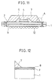
- Fig. 11 is a cross sectional view of the P-BGA and Fig. 12 is an enlarged view showing the region A of Fig. 11.
- an organic substrate 1 Shown are an organic substrate 1, a copper foil wiring pattern 2, a semiconductor chip 4, bonding wires 5, a sealing resin 7, a resist 8, a grounding layer 9, and solder paste balls 12.
- the organic substrate 1 made of e.g. bismaleic triazine resin and equipped with the copper foil wiring pattern 2 having a thickness of 10 to 40 micrometers with the resist 8 for protecting most regions of the wiring pattern 2 where no bonding wires are connected
- placing the semiconductor chip 4 by a conductive paste on the substrate 1 connecting electrodes of the semiconductor chip 4 by the bonding wires 5 to the wiring pattern 2 on the organic substrate 1, sealing with the sealing resin 7 one side of the substrate 1 where the semiconductor chip 4 is mounted, and applying a grid form of balls 12 on the other side of the substrate 1.
- the conventional P-BGA is however allows the resist 8, which contains a silicon component unfavorable for adhesivity to the sealing resin 7, to cover most regions of the organic substrate 1 to be sealed with the sealing resin 7.
- the sealing resin 7 of a particular type may cause the resist 8 to release its silicon component as triggered by a thermal history in the sealing or reflow process during the mounting to a mother board and subsequently detach at interface from the sealing resin 7, thus declining the resistance to moisture.
- a first feature of the present invention is embodied in the form of a plastic ball grid array package in which a copper sheet which has an aperture provided therein for clearing a semiconductor chip and its bonding wires is bonded to a sealing side of an organic substrate.
- a second feature of the present invention is embodied in the form of a plastic ball grip array package in which a copper sheet having a die pad formed integrally thereon for supporting a semiconductor chip is bonded by an adhesive to a sealing side of an organic substrate.
- a third feature of the present invention is embodied in the form of a plastic ball grip array package in which a copper sheet is bonded by an adhesive to a sealing side of an organic substrate and electrically connected by through holes to a grounding layer provided within the organic substrate.
- a fourth feature of the present invention is embodied in the form of a plastic ball grip array package in which a copper sheet is bonded by an adhesive to a sealing side of an organic substrate, mechanically folded at four side ends downwardly and towards the rear side of the organic substrate to cover the side edge of the organic substrate, electrically connected by through holes to the grounding layer in the organic substrate, and loaded at its folded ends with solder paste balls by platings of a nickel/gold alloy.
- a fifth feature of the present invention is embodied in the form of a plastic ball grip array package in which a copper sheet having an aperture therein is bonded by an adhesive to a sealing side of an organic substrate, electrically connected by through holes to the grounding layer in the organic substrate, and provided about the aperture with nickel/gold platings of a spot form which serve as grounding terminals.
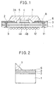
- Fig. 1 is a cross sectional view of a P-BGA (taken along the line A-A of Fig. 3) showing a first embodiment of the present invention.
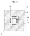
- Fig. 2 is an enlarged view of the region B of Fig. 1.
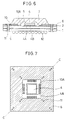
- Fig. 3 is a plan view of the P-BGA of the first embodiment viewed from the substrate sealing side.
- the P-BGA is produced by applying a copper foil wiring pattern 2 on one side of an organic substrate 1 and bonding a copper sheet of 0.1 to 0.4 mm thick, which has an aperture 6A for clearing a semiconductor chip 4 and bonding wires 5, by an adhesive 3 to the sealing side of the organic substrate 1.
- the semiconductor chip 4 is bonded by an adhesive 4B to a die pad 4A located in a predetermined region of the organic substrate 1.
- the sealing side of the organic substrate 1 of the P-BGA is covered with the copper sheet 6 which is higher in the adhesivity to the sealing resin 7 than a common resist, whereby detachment of the sealing resin 7 after the reflow process will be prevented and declination in the resistance to moisture will be minimized.
- the copper sheet 6 bonded on the sealing side of the organic substrate 1 is favorable for adhesion to the sealing resin 7 as compared with the common resist 8. This prevents the detachment of the sealing resin 7 which may result from the thermal history in the seating or reflow process and will permit no entrance of water hence minimizing declination in the resistance to moisture.
- the copper sheet 6 (of a conductive material) is located over the signal lines of the pattern thus attenuating the inductance of signals.
- Fig. 4 is a cross sectional view of a P-BGA (taken along the line B-B of Fig. 5) showing the second embodiment.
- Fig. 5 is a plan view of the P-BGA of the second embodiment viewed from the substrate sealing side.
- the second embodiment is distinguished from the first embodiment in which the copper sheet 6 bonded to the sealing side of the substrate 1 has the aperture 6A therein for providing a bonding area of the semiconductor chip 4 and its bonding wires 5 by the fact that apertures are made for clearing only the bonding wires 5 while a die pad 6B on which the semiconductor chip 4 is mounted is formed integral with the copper sheet 6.
- the copper sheet 6 having the die pad 6B formed integrally thereon for supporting the semiconductor chip 4 is bonded on the sealing side of the organic substrate 1 of the P-BGA, its high adhesivity to the sealing resin 7 prevents detachment from the sealing resin 7 after the sealing or reflow process and will minimize declination in the resistance to moisture.
- the copper sheet 6 formed integral with the die pad 6B on which the semiconductor chip 4 is mounted has heat radiator passages 6C thereon for releasing heat generated by the semiconductor chip 4 hence decreasing the thermal resistance.
- the copper sheet 6 bonded on the sealing side of the organic substrate 1 is favorable for adhesion to the sealing resin 7 as compared with the common resist. This prevents the detachment of the sealing resin 7 which may result from the thermal history in the seating or reflow process and will permit no entrance of water hence minimizing declination in the resistance to moisture.
- the heat generated by the semiconductor chip 4 can be dissipated along the die pad 6B and the heat radiator passages 6C to the copper sheet 6 hence improving the efficiency of heat radiation and allowing a high power consumption type of the semiconductor chip 4 to be employed.
- denoted by 2A are bonding terminals.
- Fig. 6 is a cross sectional view of a P-BGA (taken along the line C-C of Fig. 7) showing the third embodiment.
- Fig. 7 is a plan view of the P-BGA of the third embodiment viewed from the substrate sealing side.
- the copper sheet 6 of 0.1 to 0.4 mm thick is bonded by an adhesive 3 to the sealing side of the organic substrate 1 after a pattern of signal lines 10 made from copper foil are placed on the sealing side of the organic substrate 1.
- the copper sheet 6 is electrically connected by through holes 11 to a grounding layer 9 provided within the organic substrate 1.
- the sealing side of the organic substrate 1 of the P-BGA is covered with the copper sheet 6 which is higher in the adhesivity to the sealing resin 7 than a common resist 8, whereby detachment of the sealing resin 7 after the reflow process will be prevented and declination in the resistance to moisture will be minimized.
- the signal lines 10 between the copper sheet 6 and the grounding layer 9 are subjected to a grounding potential hence enhancing the electrical characteristics.
- Fig. 6, denoted by 10A are bonding terminals.
- the copper sheet 6 bonded on the sealing side of the organic substrate 1 is favorable for adhesion to the sealing resin 7 as compared with the common resist 8. This prevents the detachment of the sealing resin 7 which may result from the thermal history in the seating or reflow process and will permit no entrance of water hence minimizing declination in the resistance to moisture.
- the copper sheet 6 electrically connected by the through holes 11 to the grounding layer 9 provided within the organic substrate 1 allows the signal lines 10 between the copper sheet 6 and the grounding layer 9 to be subjected to a grounding potential (in a strip-line structure).
- a grounding potential in a strip-line structure.
- Fig. 8 is a cross sectional view of a P-BGA showing the fourth embodiment of the present invention.
- the copper sheet 6 of 0.1 to 0.4 mm thick is bonded by an adhesive 3 to the sealing side of the organic substrate 1 after a pattern of copper foil wiring 2 is placed on the sealing side of the organic substrate 1. Then, the copper sheet 6 is folded at four side ends downwardly and towards the rear side of the organic substrate 1 so as to cover the side edge of the organic substrate 1.
- the copper sheet 6 is electrically connected by through holes 11 to a grounding layer 9 provided within the organic substrate 1.
- a grounding layer 9 provided within the organic substrate 1.
- Four folded ends of the copper sheet 6 at the edge of the rear side of the organic substrate 1 are plated with nickel/gold alloy and then loaded with solder paste balls 12A.
- the copper sheet 6 bonded on the sealing side of the organic substrate 1 of the P-BGA is favorable for adhesion to the sealing resin 7 as compared with the common resist 8. This prevents the detachment of the sealing resin 7 which may result from the thermal history in the seating or reflow process and will permit no entrance of water hence minimizing declination in the resistance to moisture.
- the side edge of the organic substrate 1 is also covered with the copper sheet 6 and thus prevents entrance of water from side directions increasing the resistance to moisture.
- solder paste balls 12A are mounted on the folded ends of the copper sheet 6 which is electrically connected by the through holes 11 to the grounding layer 9 provided within the organic substrate 1 hence minimizing the number of grinding terminals at the ball mounting area as compared with the conventional semiconductor device. This permits installation of a more number of I/O terminals, whereby the use of terminals per package can be optimized.
- Fig. 9 is a cross sectional view of a P-BGA showing the fifth embodiment of the present invention and Fig. 10 is an explanatory view of the advantage on the P-BGA.
- the copper sheet 6 bonded to the organic substrate as described in the third or fourth embodiment is plated with a nickel/gold alloy 16 at specific spots about the apertures (0.5 to 1.0 mm from the edge).
- the plated spots 16 serve as grinding ports and are connected by bonding wires 5 to the grinding terminals of the semiconductor chip 4.
- signal bonding wires 5s extend to signal bonding terminals 15 which are located outside the source bonding terminals 14 and the grinding terminals 13 (in an annular arrangement about a die pad) and will thus be increased in length, as shown in Fig. 10(a).
- the fifth embodiment allows the nickel/gold plated spots 16 to be formed on the copper sheet 6 on the organic substrate 1 and serve as the grounding terminals so that source bonding terminals 14 and signal bonding terminals 15 are located inwardly. As the result, bonding wires 5s extending from the signal bonding terminals 15 will be reduced in length.
- the signal bonding terminals 15 are located more inside as compared with any conventional semiconductor device and thus the bonding wires are minimized in the length, whereby the signal lines will be suppressed in the inductance and reduced in the generation of noise.
- the present invention offers the following advantages.
- the copper sheet bonded to the sealing side of the organic substrate is higher in the adhesivity to the sealing resin than any conventional resist. This prevents detachment of the sealing resin at interface which may result from the thermal history in the sealing or reflow process and eliminates entrance of water thus minimizing declination in the resistance to moisture.
- the copper sheet on the organic substrate is formed integral with the die pad on which a semiconductor chip is mounted allowing heat generated by the semiconductor chip to dissipate at higher efficiency. As the efficiency of heat radiation is increased, a higher power consumption type of the semiconductor chip can be mounted.
- the copper sheet on the organic substrate is electrically connected by the through holes to the grounding layer provided within the organic substrate hence constituting a strip line structure in which the signal lines between the copper sheet and the grounding layer are subjected to a grounding potential.
- the signal lines will be decreased in the inductance, simplified for having a desired combination of characteristic impedance, and minimized in the generation of crosstalk inbetween because of the sealing effect of the grounding potential.
- the side edge of the organic substrate is covered with the copper sheet and thus prevents entrance of water from side directions increasing the resistance to moisture.
- the solder paste balls are mounted on the folded ends of the copper sheet which is electrically connected by the through holes to the grounding layer in the organic substrate hence minimizing the number of grinding terminals at the ball mounting area as compared with the conventional semiconductor device. This permits installation of a more number of I/O terminals, whereby the use of terminals per package can be optimized.
- the grounding terminals are formed on the folded ends of the copper sheet bonded to the organic substrate so that the signal bonding terminals are located inwardly, whereby the bonding wires will be reduced in the length.
Landscapes
- Structures Or Materials For Encapsulating Or Coating Semiconductor Devices Or Solid State Devices (AREA)
- Wire Bonding (AREA)
- Die Bonding (AREA)
Applications Claiming Priority (3)
| Application Number | Priority Date | Filing Date | Title |
|---|---|---|---|
| JP2742597 | 1997-02-12 | ||
| JP27425/97 | 1997-02-12 | ||
| JP02742597A JP3483720B2 (ja) | 1997-02-12 | 1997-02-12 | 半導体装置 |
Publications (3)
| Publication Number | Publication Date |
|---|---|
| EP0863549A2 true EP0863549A2 (de) | 1998-09-09 |
| EP0863549A3 EP0863549A3 (de) | 1999-02-24 |
| EP0863549B1 EP0863549B1 (de) | 2005-05-04 |
Family
ID=12220764
Family Applications (1)
| Application Number | Title | Priority Date | Filing Date |
|---|---|---|---|
| EP97310366A Expired - Lifetime EP0863549B1 (de) | 1997-02-12 | 1997-12-19 | Halbleiteranordnung mit einem Leitersubstrat |
Country Status (6)
| Country | Link |
|---|---|
| US (1) | US6060774A (de) |
| EP (1) | EP0863549B1 (de) |
| JP (1) | JP3483720B2 (de) |
| KR (1) | KR100369879B1 (de) |
| CN (1) | CN1124649C (de) |
| DE (1) | DE69733193T2 (de) |
Cited By (2)
| Publication number | Priority date | Publication date | Assignee | Title |
|---|---|---|---|---|
| US6424047B1 (en) | 1999-02-23 | 2002-07-23 | Institute Of Microelectronics | Plastic ball grid array package for passing JEDEC Level 1 Moisture Sensitivity Test |
| SG114561A1 (en) * | 2002-08-02 | 2005-09-28 | Micron Technology Inc | Integrated circuit and method of fabricating an integrated circuit that includes a frame carrier interposer |
Families Citing this family (22)
| Publication number | Priority date | Publication date | Assignee | Title |
|---|---|---|---|---|
| US6175152B1 (en) * | 1998-06-25 | 2001-01-16 | Citizen Watch Co., Ltd. | Semiconductor device |
| US6268650B1 (en) * | 1999-05-25 | 2001-07-31 | Micron Technology, Inc. | Semiconductor device, ball grid array connection system, and method of making |
| US6773965B2 (en) * | 1999-05-25 | 2004-08-10 | Micron Technology, Inc. | Semiconductor device, ball grid array connection system, and method of making |
| US6686652B1 (en) | 2000-03-20 | 2004-02-03 | National Semiconductor | Locking lead tips and die attach pad for a leadless package apparatus and method |
| US6452255B1 (en) * | 2000-03-20 | 2002-09-17 | National Semiconductor, Corp. | Low inductance leadless package |
| US6372539B1 (en) | 2000-03-20 | 2002-04-16 | National Semiconductor Corporation | Leadless packaging process using a conductive substrate |
| US6399415B1 (en) | 2000-03-20 | 2002-06-04 | National Semiconductor Corporation | Electrical isolation in panels of leadless IC packages |
| US6534852B1 (en) * | 2000-04-11 | 2003-03-18 | Advanced Semiconductor Engineering, Inc. | Ball grid array semiconductor package with improved strength and electric performance and method for making the same |
| US6750536B2 (en) * | 2001-12-14 | 2004-06-15 | Intel Corporation | Current supply and support system for a thin package |
| JP2003229517A (ja) * | 2002-01-31 | 2003-08-15 | Fujitsu Hitachi Plasma Display Ltd | 半導体チップ実装基板及びフラットディスプレイ |
| KR100499003B1 (ko) * | 2002-12-12 | 2005-07-01 | 삼성전기주식회사 | 도금 인입선을 사용하지 않는 패키지 기판 및 그 제조 방법 |
| JP4027820B2 (ja) * | 2003-03-06 | 2007-12-26 | シャープ株式会社 | 半導体装置及びその製造方法 |
| JP4096831B2 (ja) * | 2003-07-09 | 2008-06-04 | 日産自動車株式会社 | 半導体装置の実装構造 |
| US7145249B2 (en) * | 2004-03-29 | 2006-12-05 | Intel Corporation | Semiconducting device with folded interposer |
| US7378725B2 (en) * | 2004-03-31 | 2008-05-27 | Intel Corporation | Semiconducting device with stacked dice |
| US20050285254A1 (en) * | 2004-06-23 | 2005-12-29 | Buot Joan R V | Semiconducting device having stacked dice |
| JP4503039B2 (ja) * | 2006-04-27 | 2010-07-14 | 三洋電機株式会社 | 回路装置 |
| US20080073778A1 (en) * | 2006-09-27 | 2008-03-27 | Texas Instruments Incorporated | Two-way heat extraction from packaged semiconductor chips |
| TWI315095B (en) * | 2006-10-12 | 2009-09-21 | Advanced Semiconductor Eng | Semiconductor packaging structure having electromagnetic shielding function and method for manufacturing the same |
| JP4450031B2 (ja) | 2007-08-22 | 2010-04-14 | 株式会社デンソー | 半導体部品 |
| MY165522A (en) * | 2011-01-06 | 2018-04-02 | Carsem M Sdn Bhd | Leadframe packagewith die mounted on pedetal that isolates leads |
| JP6699742B2 (ja) * | 2016-09-20 | 2020-05-27 | 三菱電機株式会社 | 半導体装置 |
Family Cites Families (5)
| Publication number | Priority date | Publication date | Assignee | Title |
|---|---|---|---|---|
| US4839713A (en) * | 1987-02-20 | 1989-06-13 | Mitsubishi Denki Kabushiki Kaisha | Package structure for semiconductor device |
| JP3414017B2 (ja) * | 1994-12-09 | 2003-06-09 | ソニー株式会社 | 半導体装置 |
| JPH08250827A (ja) * | 1995-03-08 | 1996-09-27 | Shinko Electric Ind Co Ltd | 半導体装置用パッケージ及びその製造方法並びに半導体装置 |
| US5859475A (en) * | 1996-04-24 | 1999-01-12 | Amkor Technology, Inc. | Carrier strip and molded flex circuit ball grid array |
| US5689091A (en) * | 1996-09-19 | 1997-11-18 | Vlsi Technology, Inc. | Multi-layer substrate structure |
-
1997
- 1997-02-12 JP JP02742597A patent/JP3483720B2/ja not_active Expired - Fee Related
- 1997-08-21 CN CN97117703A patent/CN1124649C/zh not_active Expired - Fee Related
- 1997-08-29 KR KR1019970043182A patent/KR100369879B1/ko not_active Expired - Fee Related
- 1997-10-31 US US08/962,115 patent/US6060774A/en not_active Expired - Lifetime
- 1997-12-19 DE DE69733193T patent/DE69733193T2/de not_active Expired - Fee Related
- 1997-12-19 EP EP97310366A patent/EP0863549B1/de not_active Expired - Lifetime
Cited By (2)
| Publication number | Priority date | Publication date | Assignee | Title |
|---|---|---|---|---|
| US6424047B1 (en) | 1999-02-23 | 2002-07-23 | Institute Of Microelectronics | Plastic ball grid array package for passing JEDEC Level 1 Moisture Sensitivity Test |
| SG114561A1 (en) * | 2002-08-02 | 2005-09-28 | Micron Technology Inc | Integrated circuit and method of fabricating an integrated circuit that includes a frame carrier interposer |
Also Published As
| Publication number | Publication date |
|---|---|
| US6060774A (en) | 2000-05-09 |
| DE69733193D1 (de) | 2005-06-09 |
| KR100369879B1 (ko) | 2003-06-18 |
| CN1124649C (zh) | 2003-10-15 |
| CN1211073A (zh) | 1999-03-17 |
| DE69733193T2 (de) | 2006-03-02 |
| JP3483720B2 (ja) | 2004-01-06 |
| EP0863549B1 (de) | 2005-05-04 |
| JPH10223672A (ja) | 1998-08-21 |
| EP0863549A3 (de) | 1999-02-24 |
| KR19980069914A (ko) | 1998-10-26 |
Similar Documents
| Publication | Publication Date | Title |
|---|---|---|
| US6060774A (en) | Semiconductor device | |
| US5929514A (en) | Thermally enhanced lead-under-paddle I.C. leadframe | |
| US6153924A (en) | Multilayered lead frame for semiconductor package | |
| JP2881575B2 (ja) | ヒートシンク付着ボールグリッドアレイ半導体パッケージ | |
| US5620928A (en) | Ultra thin ball grid array using a flex tape or printed wiring board substrate and method | |
| JP3176307B2 (ja) | 集積回路装置の実装構造およびその製造方法 | |
| US6002169A (en) | Thermally enhanced tape ball grid array package | |
| US6093960A (en) | Semiconductor package having a heat spreader capable of preventing being soldered and enhancing adhesion and electrical performance | |
| JPH08298302A (ja) | 樹脂封止型半導体装置およびその製造方法 | |
| US6822338B2 (en) | Wiring structure of semiconductor device | |
| US6316828B1 (en) | Structure of a solder mask for the circuit module of a BGA substrate | |
| JP3764214B2 (ja) | プリント回路基板およびこれを備えた電子機器 | |
| US5422515A (en) | Semiconductor module including wiring structures each having different current capacity | |
| US20050087864A1 (en) | Cavity-down semiconductor package with heat spreader | |
| JP3506547B2 (ja) | 半導体装置 | |
| JP2803656B2 (ja) | 半導体装置 | |
| JP2002057238A (ja) | 集積回路パッケージ | |
| JP3462591B2 (ja) | 混成集積回路装置 | |
| JP2735920B2 (ja) | インバータ装置 | |
| US20040021213A1 (en) | Thermally-enhanced integrated circuit package | |
| JP3062102B2 (ja) | 放熱板付きプリント基板 | |
| KR100861509B1 (ko) | 전기적 및 열적으로 향상된 반도체 패키지 | |
| JPH06260572A (ja) | 半導体装置 | |
| JP3177934B2 (ja) | マルチチップ半導体装置 | |
| JP3259217B2 (ja) | ノイズ低減パッケージ |
Legal Events
| Date | Code | Title | Description |
|---|---|---|---|
| PUAI | Public reference made under article 153(3) epc to a published international application that has entered the european phase |
Free format text: ORIGINAL CODE: 0009012 |
|
| AK | Designated contracting states |
Kind code of ref document: A2 Designated state(s): DE FR GB NL |
|
| AX | Request for extension of the european patent |
Free format text: AL;LT;LV;MK;RO;SI |
|
| PUAL | Search report despatched |
Free format text: ORIGINAL CODE: 0009013 |
|
| AK | Designated contracting states |
Kind code of ref document: A3 Designated state(s): AT BE CH DE DK ES FI FR GB GR IE IT LI LU MC NL PT SE |
|
| AX | Request for extension of the european patent |
Free format text: AL;LT;LV;MK;RO;SI |
|
| 17P | Request for examination filed |
Effective date: 19990805 |
|
| AKX | Designation fees paid |
Free format text: DE FR GB NL |
|
| 17Q | First examination report despatched |
Effective date: 20030417 |
|
| GRAP | Despatch of communication of intention to grant a patent |
Free format text: ORIGINAL CODE: EPIDOSNIGR1 |
|
| GRAS | Grant fee paid |
Free format text: ORIGINAL CODE: EPIDOSNIGR3 |
|
| GRAA | (expected) grant |
Free format text: ORIGINAL CODE: 0009210 |
|
| AK | Designated contracting states |
Kind code of ref document: B1 Designated state(s): DE FR GB NL |
|
| REG | Reference to a national code |
Ref country code: GB Ref legal event code: FG4D |
|
| REF | Corresponds to: |
Ref document number: 69733193 Country of ref document: DE Date of ref document: 20050609 Kind code of ref document: P |
|
| PGFP | Annual fee paid to national office [announced via postgrant information from national office to epo] |
Ref country code: FR Payment date: 20051017 Year of fee payment: 9 |
|
| PGFP | Annual fee paid to national office [announced via postgrant information from national office to epo] |
Ref country code: GB Payment date: 20051205 Year of fee payment: 9 |
|
| PGFP | Annual fee paid to national office [announced via postgrant information from national office to epo] |
Ref country code: NL Payment date: 20051223 Year of fee payment: 9 |
|
| PGFP | Annual fee paid to national office [announced via postgrant information from national office to epo] |
Ref country code: DE Payment date: 20060227 Year of fee payment: 9 |
|
| PLBE | No opposition filed within time limit |
Free format text: ORIGINAL CODE: 0009261 |
|
| STAA | Information on the status of an ep patent application or granted ep patent |
Free format text: STATUS: NO OPPOSITION FILED WITHIN TIME LIMIT |
|
| ET | Fr: translation filed | ||
| 26N | No opposition filed |
Effective date: 20060207 |
|
| PG25 | Lapsed in a contracting state [announced via postgrant information from national office to epo] |
Ref country code: NL Free format text: LAPSE BECAUSE OF NON-PAYMENT OF DUE FEES Effective date: 20070701 |
|
| PG25 | Lapsed in a contracting state [announced via postgrant information from national office to epo] |
Ref country code: DE Free format text: LAPSE BECAUSE OF NON-PAYMENT OF DUE FEES Effective date: 20070703 |
|
| GBPC | Gb: european patent ceased through non-payment of renewal fee |
Effective date: 20061219 |
|
| NLV4 | Nl: lapsed or anulled due to non-payment of the annual fee |
Effective date: 20070701 |
|
| REG | Reference to a national code |
Ref country code: FR Ref legal event code: ST Effective date: 20070831 |
|
| PG25 | Lapsed in a contracting state [announced via postgrant information from national office to epo] |
Ref country code: GB Free format text: LAPSE BECAUSE OF NON-PAYMENT OF DUE FEES Effective date: 20061219 |
|
| PG25 | Lapsed in a contracting state [announced via postgrant information from national office to epo] |
Ref country code: FR Free format text: LAPSE BECAUSE OF NON-PAYMENT OF DUE FEES Effective date: 20070102 |