EP0860860A2 - Vorrichtung zum Behandeln von Wafern, Verfahren zum Behandeln von Wafern und Verfahren zur Herstellung eines Halbleitersubstrats - Google Patents
Vorrichtung zum Behandeln von Wafern, Verfahren zum Behandeln von Wafern und Verfahren zur Herstellung eines Halbleitersubstrats Download PDFInfo
- Publication number
- EP0860860A2 EP0860860A2 EP98102897A EP98102897A EP0860860A2 EP 0860860 A2 EP0860860 A2 EP 0860860A2 EP 98102897 A EP98102897 A EP 98102897A EP 98102897 A EP98102897 A EP 98102897A EP 0860860 A2 EP0860860 A2 EP 0860860A2
- Authority
- EP
- European Patent Office
- Prior art keywords
- wafer
- substrate
- processing
- layer
- porous layer
- Prior art date
- Legal status (The legal status is an assumption and is not a legal conclusion. Google has not performed a legal analysis and makes no representation as to the accuracy of the status listed.)
- Withdrawn
Links
- 239000000758 substrate Substances 0.000 title claims description 160
- 238000000034 method Methods 0.000 title claims description 53
- 238000004519 manufacturing process Methods 0.000 title claims description 25
- 239000004065 semiconductor Substances 0.000 title claims description 21
- 238000003672 processing method Methods 0.000 title claims description 18
- 235000012431 wafers Nutrition 0.000 claims abstract description 395
- 238000005530 etching Methods 0.000 claims description 87
- KRHYYFGTRYWZRS-UHFFFAOYSA-N Fluorane Chemical compound F KRHYYFGTRYWZRS-UHFFFAOYSA-N 0.000 claims description 76
- 229910021426 porous silicon Inorganic materials 0.000 claims description 59
- VYPSYNLAJGMNEJ-UHFFFAOYSA-N silicon dioxide Inorganic materials O=[Si]=O VYPSYNLAJGMNEJ-UHFFFAOYSA-N 0.000 claims description 54
- 229910021421 monocrystalline silicon Inorganic materials 0.000 claims description 45
- MHAJPDPJQMAIIY-UHFFFAOYSA-N Hydrogen peroxide Chemical compound OO MHAJPDPJQMAIIY-UHFFFAOYSA-N 0.000 claims description 38
- 239000000203 mixture Substances 0.000 claims description 27
- 239000002245 particle Substances 0.000 claims description 26
- 230000007246 mechanism Effects 0.000 claims description 22
- QTBSBXVTEAMEQO-UHFFFAOYSA-N Acetic acid Chemical compound CC(O)=O QTBSBXVTEAMEQO-UHFFFAOYSA-N 0.000 claims description 21
- 238000004140 cleaning Methods 0.000 claims description 19
- LFQSCWFLJHTTHZ-UHFFFAOYSA-N Ethanol Chemical compound CCO LFQSCWFLJHTTHZ-UHFFFAOYSA-N 0.000 claims description 15
- 230000005540 biological transmission Effects 0.000 claims description 14
- 238000011109 contamination Methods 0.000 claims description 12
- 238000007598 dipping method Methods 0.000 claims description 12
- XUIMIQQOPSSXEZ-UHFFFAOYSA-N Silicon Chemical compound [Si] XUIMIQQOPSSXEZ-UHFFFAOYSA-N 0.000 claims description 10
- 229910052710 silicon Inorganic materials 0.000 claims description 10
- 239000010703 silicon Substances 0.000 claims description 10
- 239000010453 quartz Substances 0.000 claims description 9
- GRYLNZFGIOXLOG-UHFFFAOYSA-N Nitric acid Chemical compound O[N+]([O-])=O GRYLNZFGIOXLOG-UHFFFAOYSA-N 0.000 claims description 7
- 229910017604 nitric acid Inorganic materials 0.000 claims description 7
- 239000004696 Poly ether ether ketone Substances 0.000 claims description 6
- 229920001707 polybutylene terephthalate Polymers 0.000 claims description 6
- 229920002530 polyetherether ketone Polymers 0.000 claims description 6
- -1 polyethylene Polymers 0.000 claims description 6
- 239000000463 material Substances 0.000 claims description 5
- 229910052814 silicon oxide Inorganic materials 0.000 claims description 5
- YCKRFDGAMUMZLT-UHFFFAOYSA-N Fluorine atom Chemical compound [F] YCKRFDGAMUMZLT-UHFFFAOYSA-N 0.000 claims description 4
- 150000001875 compounds Chemical class 0.000 claims description 4
- 239000000470 constituent Substances 0.000 claims description 4
- 229910052731 fluorine Inorganic materials 0.000 claims description 4
- 239000011737 fluorine Substances 0.000 claims description 4
- 230000002093 peripheral effect Effects 0.000 claims description 4
- 239000004033 plastic Substances 0.000 claims description 4
- 229920003023 plastic Polymers 0.000 claims description 4
- 238000005498 polishing Methods 0.000 claims description 4
- 239000011347 resin Substances 0.000 claims description 4
- 229920005989 resin Polymers 0.000 claims description 4
- 239000004698 Polyethylene Substances 0.000 claims description 3
- 239000004743 Polypropylene Substances 0.000 claims description 3
- BZHJMEDXRYGGRV-UHFFFAOYSA-N Vinyl chloride Chemical compound ClC=C BZHJMEDXRYGGRV-UHFFFAOYSA-N 0.000 claims description 3
- 238000000227 grinding Methods 0.000 claims description 3
- 229920000573 polyethylene Polymers 0.000 claims description 3
- 229920001155 polypropylene Polymers 0.000 claims description 3
- 229910052681 coesite Inorganic materials 0.000 description 20
- 229910052906 cristobalite Inorganic materials 0.000 description 20
- 239000000377 silicon dioxide Substances 0.000 description 20
- 229910052682 stishovite Inorganic materials 0.000 description 20
- 229910052905 tridymite Inorganic materials 0.000 description 20
- 238000010276 construction Methods 0.000 description 9
- 238000010438 heat treatment Methods 0.000 description 7
- 229910021642 ultra pure water Inorganic materials 0.000 description 7
- 239000012498 ultrapure water Substances 0.000 description 7
- 239000007789 gas Substances 0.000 description 6
- 230000008569 process Effects 0.000 description 6
- UFHFLCQGNIYNRP-UHFFFAOYSA-N Hydrogen Chemical compound [H][H] UFHFLCQGNIYNRP-UHFFFAOYSA-N 0.000 description 5
- 229910052581 Si3N4 Inorganic materials 0.000 description 5
- 238000005229 chemical vapour deposition Methods 0.000 description 5
- 239000001257 hydrogen Substances 0.000 description 5
- 229910052739 hydrogen Inorganic materials 0.000 description 5
- 238000007254 oxidation reaction Methods 0.000 description 5
- 239000011148 porous material Substances 0.000 description 5
- QGZKDVFQNNGYKY-UHFFFAOYSA-N Ammonia Chemical compound N QGZKDVFQNNGYKY-UHFFFAOYSA-N 0.000 description 4
- NBIIXXVUZAFLBC-UHFFFAOYSA-N Phosphoric acid Chemical compound OP(O)(O)=O NBIIXXVUZAFLBC-UHFFFAOYSA-N 0.000 description 4
- 230000003647 oxidation Effects 0.000 description 4
- 230000003746 surface roughness Effects 0.000 description 4
- 229910001868 water Inorganic materials 0.000 description 4
- 229910001218 Gallium arsenide Inorganic materials 0.000 description 3
- 238000007743 anodising Methods 0.000 description 3
- 239000013078 crystal Substances 0.000 description 3
- 229910003818 SiH2Cl2 Inorganic materials 0.000 description 2
- 229910000147 aluminium phosphate Inorganic materials 0.000 description 2
- 229910021529 ammonia Inorganic materials 0.000 description 2
- 238000002048 anodisation reaction Methods 0.000 description 2
- QVGXLLKOCUKJST-UHFFFAOYSA-N atomic oxygen Chemical compound [O] QVGXLLKOCUKJST-UHFFFAOYSA-N 0.000 description 2
- 230000007547 defect Effects 0.000 description 2
- 239000001301 oxygen Substances 0.000 description 2
- 229910052760 oxygen Inorganic materials 0.000 description 2
- 239000002033 PVDF binder Substances 0.000 description 1
- 239000004813 Perfluoroalkoxy alkane Substances 0.000 description 1
- 230000009471 action Effects 0.000 description 1
- 238000013019 agitation Methods 0.000 description 1
- 229910021417 amorphous silicon Inorganic materials 0.000 description 1
- 238000000137 annealing Methods 0.000 description 1
- 230000015572 biosynthetic process Effects 0.000 description 1
- 230000000694 effects Effects 0.000 description 1
- 238000001914 filtration Methods 0.000 description 1
- 239000011521 glass Substances 0.000 description 1
- 230000002209 hydrophobic effect Effects 0.000 description 1
- 239000007788 liquid Substances 0.000 description 1
- 239000007791 liquid phase Substances 0.000 description 1
- 239000002184 metal Substances 0.000 description 1
- 238000002156 mixing Methods 0.000 description 1
- 238000012986 modification Methods 0.000 description 1
- 230000004048 modification Effects 0.000 description 1
- 238000001451 molecular beam epitaxy Methods 0.000 description 1
- 230000001590 oxidative effect Effects 0.000 description 1
- 229920011301 perfluoro alkoxyl alkane Polymers 0.000 description 1
- 229910021420 polycrystalline silicon Inorganic materials 0.000 description 1
- 239000004810 polytetrafluoroethylene Substances 0.000 description 1
- 229920001343 polytetrafluoroethylene Polymers 0.000 description 1
- 229920002981 polyvinylidene fluoride Polymers 0.000 description 1
- 229910052594 sapphire Inorganic materials 0.000 description 1
- 239000010980 sapphire Substances 0.000 description 1
- 238000004544 sputter deposition Methods 0.000 description 1
- 239000000126 substance Substances 0.000 description 1
- 239000002887 superconductor Substances 0.000 description 1
- 238000004381 surface treatment Methods 0.000 description 1
- 230000008646 thermal stress Effects 0.000 description 1
- XLYOFNOQVPJJNP-UHFFFAOYSA-N water Substances O XLYOFNOQVPJJNP-UHFFFAOYSA-N 0.000 description 1
Images


Classifications
-
- H—ELECTRICITY
- H01—ELECTRIC ELEMENTS
- H01L—SEMICONDUCTOR DEVICES NOT COVERED BY CLASS H10
- H01L21/00—Processes or apparatus adapted for the manufacture or treatment of semiconductor or solid state devices or of parts thereof
- H01L21/67—Apparatus specially adapted for handling semiconductor or electric solid state devices during manufacture or treatment thereof; Apparatus specially adapted for handling wafers during manufacture or treatment of semiconductor or electric solid state devices or components ; Apparatus not specifically provided for elsewhere
- H01L21/67005—Apparatus not specifically provided for elsewhere
- H01L21/67011—Apparatus for manufacture or treatment
- H01L21/67017—Apparatus for fluid treatment
- H01L21/67028—Apparatus for fluid treatment for cleaning followed by drying, rinsing, stripping, blasting or the like
- H01L21/6704—Apparatus for fluid treatment for cleaning followed by drying, rinsing, stripping, blasting or the like for wet cleaning or washing
- H01L21/67057—Apparatus for fluid treatment for cleaning followed by drying, rinsing, stripping, blasting or the like for wet cleaning or washing with the semiconductor substrates being dipped in baths or vessels
-
- H—ELECTRICITY
- H01—ELECTRIC ELEMENTS
- H01L—SEMICONDUCTOR DEVICES NOT COVERED BY CLASS H10
- H01L21/00—Processes or apparatus adapted for the manufacture or treatment of semiconductor or solid state devices or of parts thereof
- H01L21/02—Manufacture or treatment of semiconductor devices or of parts thereof
- H01L21/04—Manufacture or treatment of semiconductor devices or of parts thereof the devices having potential barriers, e.g. a PN junction, depletion layer or carrier concentration layer
- H01L21/18—Manufacture or treatment of semiconductor devices or of parts thereof the devices having potential barriers, e.g. a PN junction, depletion layer or carrier concentration layer the devices having semiconductor bodies comprising elements of Group IV of the Periodic Table or AIIIBV compounds with or without impurities, e.g. doping materials
- H01L21/30—Treatment of semiconductor bodies using processes or apparatus not provided for in groups H01L21/20 - H01L21/26
- H01L21/302—Treatment of semiconductor bodies using processes or apparatus not provided for in groups H01L21/20 - H01L21/26 to change their surface-physical characteristics or shape, e.g. etching, polishing, cutting
- H01L21/304—Mechanical treatment, e.g. grinding, polishing, cutting
-
- B—PERFORMING OPERATIONS; TRANSPORTING
- B08—CLEANING
- B08B—CLEANING IN GENERAL; PREVENTION OF FOULING IN GENERAL
- B08B3/00—Cleaning by methods involving the use or presence of liquid or steam
- B08B3/04—Cleaning involving contact with liquid
- B08B3/10—Cleaning involving contact with liquid with additional treatment of the liquid or of the object being cleaned, e.g. by heat, by electricity or by vibration
- B08B3/12—Cleaning involving contact with liquid with additional treatment of the liquid or of the object being cleaned, e.g. by heat, by electricity or by vibration by sonic or ultrasonic vibrations
-
- H—ELECTRICITY
- H01—ELECTRIC ELEMENTS
- H01L—SEMICONDUCTOR DEVICES NOT COVERED BY CLASS H10
- H01L21/00—Processes or apparatus adapted for the manufacture or treatment of semiconductor or solid state devices or of parts thereof
- H01L21/02—Manufacture or treatment of semiconductor devices or of parts thereof
- H01L21/04—Manufacture or treatment of semiconductor devices or of parts thereof the devices having potential barriers, e.g. a PN junction, depletion layer or carrier concentration layer
- H01L21/18—Manufacture or treatment of semiconductor devices or of parts thereof the devices having potential barriers, e.g. a PN junction, depletion layer or carrier concentration layer the devices having semiconductor bodies comprising elements of Group IV of the Periodic Table or AIIIBV compounds with or without impurities, e.g. doping materials
- H01L21/20—Deposition of semiconductor materials on a substrate, e.g. epitaxial growth solid phase epitaxy
- H01L21/2003—Deposition of semiconductor materials on a substrate, e.g. epitaxial growth solid phase epitaxy characterised by the substrate
- H01L21/2007—Bonding of semiconductor wafers to insulating substrates or to semiconducting substrates using an intermediate insulating layer
-
- H—ELECTRICITY
- H01—ELECTRIC ELEMENTS
- H01L—SEMICONDUCTOR DEVICES NOT COVERED BY CLASS H10
- H01L21/00—Processes or apparatus adapted for the manufacture or treatment of semiconductor or solid state devices or of parts thereof
- H01L21/02—Manufacture or treatment of semiconductor devices or of parts thereof
- H01L21/04—Manufacture or treatment of semiconductor devices or of parts thereof the devices having potential barriers, e.g. a PN junction, depletion layer or carrier concentration layer
- H01L21/18—Manufacture or treatment of semiconductor devices or of parts thereof the devices having potential barriers, e.g. a PN junction, depletion layer or carrier concentration layer the devices having semiconductor bodies comprising elements of Group IV of the Periodic Table or AIIIBV compounds with or without impurities, e.g. doping materials
- H01L21/30—Treatment of semiconductor bodies using processes or apparatus not provided for in groups H01L21/20 - H01L21/26
- H01L21/302—Treatment of semiconductor bodies using processes or apparatus not provided for in groups H01L21/20 - H01L21/26 to change their surface-physical characteristics or shape, e.g. etching, polishing, cutting
- H01L21/306—Chemical or electrical treatment, e.g. electrolytic etching
- H01L21/30604—Chemical etching
- H01L21/30608—Anisotropic liquid etching
-
- Y—GENERAL TAGGING OF NEW TECHNOLOGICAL DEVELOPMENTS; GENERAL TAGGING OF CROSS-SECTIONAL TECHNOLOGIES SPANNING OVER SEVERAL SECTIONS OF THE IPC; TECHNICAL SUBJECTS COVERED BY FORMER USPC CROSS-REFERENCE ART COLLECTIONS [XRACs] AND DIGESTS
- Y10—TECHNICAL SUBJECTS COVERED BY FORMER USPC
- Y10S—TECHNICAL SUBJECTS COVERED BY FORMER USPC CROSS-REFERENCE ART COLLECTIONS [XRACs] AND DIGESTS
- Y10S134/00—Cleaning and liquid contact with solids
- Y10S134/902—Semiconductor wafer
Definitions
- the present invention relates to a wafer processing apparatus, a wafer processing method, and a semiconductor substrate fabrication method and, more particularly, to a wafer processing apparatus for processing a wafer by dipping it into a processing solution, a wafer processing method, and a semiconductor substrate fabrication method.
- Cleaning processing is a typical example of wafer processing.
- One subject of wafer cleaning is to increase the speed.
- Japanese Patent Laid-Open No. 8-293478 has disclosed a wafer cleaning method capable of increasing the cleaning efficiency by supplying ultrasonic waves while rotating a wafer, and an apparatus for practicing this method.
- the wafer cleaning method disclosed in Japanese Patent Laid-Open No. 8-293478 is based on the recognition that a wafer is most efficiently cleaned at the interface between a cleaning solution and ambient atmosphere. In the wafer cleaning method, therefore, particles inevitably attach to a wafer at the interface between the cleaning solution and ambient atmosphere.
- a wafer processing apparatus is a wafer processing apparatus for processing a wafer by dipping the wafer into a processing solution, characterized by comprising a processing bath having a depth that allows to completely dip the wafer into the processing solution, wafer rotating means for rotating one or a plurality of wafers held by a wafer holder by using a wafer rotating member which rotates about a shaft shifted from a portion immediately below a barycenter of the one or plurality of wafers, and ultrasonic generating means for generating ultrasonic waves in the processing bath.
- the wafer rotating member is preferably arranged as a member for transmitting a rotating force to the wafer below the one or plurality of wafers held by the wafer holder.
- the wafer rotating member preferably comprises at least one rod member substantially parallel to the shaft, and the rod member preferably rotates about the shaft.
- the rod member preferably has a diameter much smaller than a diameter of a cylinder virtually formed upon rotation of the rod member about the shaft.
- the rod member preferably has a groove which engages with a peripheral portion of the wafer.
- a section of the rod member taken along the shaft preferably has a substantially sine-wave shape.
- a section of the rod member taken along the shaft preferably has a substantially full-wave rectifying shape.
- the wafer rotating means preferably further comprises driving force generating means arranged outside the processing bath, and driving force transmission means for transmitting a driving force generated by the driving force generating means to the wafer rotating member and rotating the wafer rotating member.
- the wafer processing apparatus preferably further comprises a dividing member for dividing an interior of the processing bath into a processing wafer side and a side of the driving force transmission means.
- the driving force transmission means preferably transmits the driving force generated by the driving force generating means through a crank mechanism.
- the processing bath preferably comprises a circulating mechanism having an overflow bath.
- the circulating mechanism preferably comprises contamination reducing means for reducing contamination of the wafer by particles.
- the contamination reducing means preferably comprises a filter.
- the contamination reducing means preferably comprises means for adjusting flow of the processing solution in the processing bath.
- the ultrasonic generating means preferably comprises an ultrasonic bath and an ultrasonic source, and the processing bath preferably receives ultrasonic waves through an ultrasonic transmitting medium sat in the ultrasonic bath.
- the wafer processing apparatus preferably further comprises driving means for changing a relative positional relationship between the ultrasonic source and a wafer to be processed.
- the driving means preferably moves the ultrasonic source within the ultrasonic bath.
- At least portions of constituent members of the processing bath and the wafer rotating means which may come into contact with the processing solution are preferably made of one material selected from the group consisting of quartz and plastic.
- At least portions of constituent members of the processing bath and the wafer rotating means which may come into contact with the processing solution are preferably made of one material selected from the group consisting of a fluorine resin, vinyl chloride, polyethylene, polypropylene, polybutyleneterephthalate (PBT), and polyetheretherketone (PEEK).
- a wafer processing method is a wafer processing method of processing a wafer while ultrasonic waves are supplied, characterized by comprising processing the wafer while entirely dipping the wafer into a processing solution and rotating the wafer.
- a wafer processing method is a wafer processing method of processing a wafer while ultrasonic waves are supplied, characterized by comprising processing the wafer while entirely dipping the wafer into a processing solution, and rotating and vertically moving the wafer.
- a wafer processing method is a wafer processing method of processing a wafer while ultrasonic waves are supplied, characterized by comprising processing the wafer while entirely dipping the wafer into a processing solution and changing a position of an ultrasonic source.
- the wafer processing method according to the present invention is characterized in that the wafer is cleaned using a wafer cleaning solution as the processing solution.
- the wafer processing method is suitable for a method of etching the wafer using a wafer etching solution as the processing solution.
- the wafer processing method is suitable for a method of etching a porous silicon layer of a wafer having the porous silicon layer using a porous silicon etching solution as the processing solution.
- the wafer processing method is suitable for a method of etching a porous silicon layer of a wafer having the porous silicon layer using, as the processing solution, any one of
- a semiconductor substrate fabrication method is characterized by comprising the step of forming a non porous layer on a porous layer formed on a surface of a first substrate, the step of bonding a first substrate side of a prospective structure and a second substrate prepared separately to sandwich the non porous layer between the first substrate side and the second substrate, the removal step of removing the first substrate from the bonded structure to expose the porous layer on a second substrate side thereof, and the etching step of etching the porous layer while the second substrate side on which the porous layer is exposed is completely dipped into an etching solution, and ultrasonic waves are supplied, thereby exposing surface of the second substrate side, the etching step rotating the second substrate side.
- a semiconductor substrate fabrication method is characterized by comprising the step of forming a non porous layer on a porous layer formed on a surface of a first substrate, the step of bonding a first substrate side of a prospective structure and a second substrate prepared separately to sandwich the non porous layer between the first substrate side and the second substrate, the removal step of removing the first substrate from the bonded structure to expose the porous layer on a second substrate side thereof, and the etching step of etching the porous layer while the second substrate side on which the porous layer is exposed is completely dipped into an etching solution, and ultrasonic waves are supplied, thereby exposing surface of the second substrate side, the etching step rotating and vertically moving the second substrate side.
- a semiconductor substrate fabrication method is characterized by comprising the step of forming a non porous layer on a porous layer formed on a surface of a first substrate, the step of bonding a first substrate side of a prospective structure and a second substrate prepared separately to sandwich the non porous layer between the first substrate side and the second substrate, the removal step of removing the first substrate from the bonded structure to expose the porous layer on a second substrate side thereof, and the etching step of etching the porous layer while the second substrate side on which the porous layer is exposed is completely dipped into an etching solution, and ultrasonic waves are supplied, thereby exposing surface of the second substrate side, the etching step changing a position of an ultrasonic bath.
- the etching solution used in the etching step is preferably any one of
- the removal step preferably comprises exposing the porous layer by grinding, polishing, or etching the first substrate from a back surface.
- the removal step preferably comprises separating the first substrate side and the second substrate side at a boundary of the porous layer.
- the non porous layer is preferably a single-crystal silicon layer.
- the non porous layer is preferably made up of a single-crystal silicon layer and a silicon oxide layer formed on the single-crystal silicon layer.
- the non porous layer is preferably a compound semiconductor layer.
- the second substrate is preferably a silicon substrate.
- the second substrate is preferably a silicon substrate having a silicon oxide film formed on a surface to be bonded to the first substrate side.
- the second substrate is preferably a light-transmitting substrate.
- Fig. 1 is a perspective view showing the schematic construction of a wafer processing apparatus according to the first embodiment of the present invention.
- Fig. 2 is a sectional view of the wafer processing apparatus shown in Fig. 1.
- portions which may come into contact with a processing solution are preferably made from quartz or plastic in accordance with the intended use.
- the plastic are a fluorine resin, vinyl chloride, polyethylene, polypropylene, polybutyleneterephthalate (PBT), and polyetheretherketone (PEEK).
- the fluorine resin are PVDF, PFA, and PTFE.
- This wafer processing apparatus 100 has a wafer processing bath 10, an overflow bath 20, an ultrasonic bath 30, and a wafer rotating mechanism (52 to 59) for rotating wafers 40.
- the wafer processing bath 10 is filled with a processing solution (e.g., an etching solution or a cleaning solution).
- a processing solution e.g., an etching solution or a cleaning solution.
- the overflow bath 20 for temporarily storing any processing solution overflowing from the wafer processing bath 10 is provided around the upper portion of the wafer processing bath 10.
- the processing solution temporarily stored in the overflow bath 20 is discharged from the bottom portion of the overflow bath 20 to a circulator 21 through a discharge pipe 21a.
- the circulator 21 removes particles by filtering the discharged processing solution and supplies the processing solution to the bottom portion of the wafer processing bath 10 through a supply pipe 21b. Consequently, particles in the wafer processing bath 10 are efficiently removed.
- the wafer processing bath 10 must have a depth by which the wafers 40 are completely dipped. This prevents particles from attaching to the wafers 40 at the interface between the processing solution and ambient atmosphere, and makes processing for the wafers 40 uniform.
- the ultrasonic bath 30 is arranged below the wafer processing bath 10.
- An ultrasonic source 31 is supported by an adjusting mechanism 32 inside the ultrasonic bath 30.
- This adjusting mechanism 32 includes a mechanism for adjusting the vertical position of the ultrasonic source 31 and a mechanism for adjusting the horizontal position of the ultrasonic source 31, as mechanisms for adjusting the relative positional relationship between the ultrasonic source 31 and the wafer processing bath 10 (wafers 40).
- the ultrasonic source 31 preferably has a function of adjusting the frequency or strength of ultrasonic waves to be generated. This further optimizes the supply of ultrasonic waves.
- the apparatus thus has the mechanism for optimizing the supply of ultrasonic waves to the wafers 40, various types of wafers can be processed. Swinging the ultrasonic source 31 by the adjusting mechanism 32 while the wafers 40 are processed can make processing for the wafers 40 uniform. Changing the frequency of ultrasonic waves while the wafers 40 are processed can also make processing for the wafers 40 uniform.
- the ultrasonic bath 30 is filled with an ultrasonic transmitting medium (e.g., water), and this ultrasonic transmitting medium transmits ultrasonic waves to the wafer processing bath 10.
- an ultrasonic transmitting medium e.g., water
- the wafers 40 are held to be nearly perpendicular to the bottom surface of the wafer processing bath 10 by a wafer holder 41.
- the wafer holder 41 is detachable from the wafer processing bath 10.
- the wafer holder 41 is suitably a carrier cassette generally used.
- the wafer holder 41 is set at a predetermined position by positioning members 42 fixed to the bottom surface of the wafer processing bath 10.
- FIG. 3 is a perspective view showing an example of the construction of the wafer rotating member 50.
- the wafer rotating member 50 In the wafer rotating member 50, two wafer rotating rods 53 arranged substantially parallel to each other are coupled through connecting rods 54, and a rotating shaft 52 is coupled to almost the center of one connecting rod 54.
- the wafer rotating member 50 is pivotally supported at the rotating shaft 52 by a shaft support portion 11. Note that another rotating shaft may be arranged on the side opposite to the rotating shaft 52.
- the diameter of the wafer rotating rod 53 is set much smaller than the diameter of a cylinder virtually formed upon rotation of the wafer rotating rods 53. With this setting, the transmission efficiency of a rotating torque and ultrasonic waves to the wafers 40 can be increased.
- Standing waves i.e., high- and low-strength portions of ultrasonic waves are usually formed between the bottom surface of the wafer processing bath 10 and the liquid surface.
- processing for the wafers 40 can be made uniform because the wafers 40 are rotated while being vertically moved by rotation of the wafer rotating member 50.
- the wafer rotating member 50 Since the wafer rotating member 50 has the minimum member which interrupts the transmission of ultrasonic waves between the bottom surface of the wafer processing bath 10 and the wafers 40, the transmission efficiency of ultrasonic waves to the wafers 40 can be greatly increased.
- the wafer rotating member 50 also has a function of agitating the processing solution. This agitation also makes processing for the wafers 40 uniform.
- the wafer rotating rod 53 preferably has a shape that allows an increase in frictional force when it comes into contact with the wafers 40, in order to prevent the wafers 40 and the wafer rotating rod 53 from slipping upon applying ultrasonic waves.
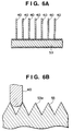
- Figs. 6A and 6B are sectional views, respectively, showing another example of the construction of the wafer rotating rod 53.
- the wafer rotating rod 53 has many V-shaped grooves 53a in a saw form which engage with the wafers 40. By forming the surface of the wafer rotating rod 53 into such a shape as to pinch the wafers 40, a slip between the wafers 40 and the wafer rotating rod 53 can be suppressed upon applying ultrasonic waves.
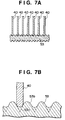
- Figs. 7A and 7B are sectional views, respectively, showing still another example of the construction of the wafer rotating rod 53.
- the section of this wafer rotating rod 53 has a sine-wave shape.
- the wafer rotating rod 53 can come into substantially surface contact with the peripheral portions of the wafers 40, and can pinch the wafers 40. Therefore, a slip between the wafers 40 and the wafer rotating rod 53 is more effectively suppressed upon applying ultrasonic waves.
- this wafer rotating rod 53 does not have any acute-angled portion, unlike the wafer rotating rod 53 shown in Figs. 6A and 6B, particles produced upon contact with the wafers 40 can be reduced. This effect can also be achieved by forming grooves 53c with a full-wave rectifying shape.
- Figs. 8A, 8B, and 8C are views each showing an example of the shape of the section of the wafer rotating rod 53.
- the section of the wafer rotating rod 53 can have various shapes. For example, its section may have a circular shape as shown in Fig. 8A, an elliptic shape as shown in Fig. 8B, or a shape as shown in Fig. 8C.
- the rotating shaft 52 of the wafer rotating member 50 is preferably shifted from a position immediately below the barycenter of the wafers 40 toward the side wall of the wafer holder 41 (x-axis direction)
- the rotational direction of the wafer rotating rods 53 is not particularly limited, it is preferably a direction to lift the wafers 40 by the wafer rotating rod 53 closer to a position immediately below the barycenter of the wafers 40 (to be referred to as the lifting direction hereinafter), as shown in Fig. 2. This is because, if the wafer rotating rods 53 are rotated in the lifting direction, a force acts on the wafers 40 substantially vertically, and hence friction between the wafers 40 and the side wall of the wafer holder 41 becomes small.
- Figs. 4A and 4B are views, respectively, showing the movement of the wafer 40 upon rotating the wafer rotating member 50 in the lifting direction.
- a direction A shows the lifting direction
- a direction B shows the rotational direction of the wafer 40.
- the wafer 40 rotates in the direction B from the state in Fig. 4A while being substantially vertically lifted by the wafer rotating rod 53 on a side immediately below the barycenter of the wafer 40.
- the wafer 40 passes through the state shown in Fig. 4B, and returns to the state shown in Fig. 4A after the wafer rotating rods 53 rotate through 180°. Accordingly, the wafer 40 rotates while swinging vertically.
- Figs. 5A and 5B are views, respectively, showing the movement of a wafer 40 having an orientation flat.
- the number of wafer rotating rods 53 is preferably two, as described above. However, the number of wafer rotating rods 53 may be one. Also in this case, the wafer 40 can be rotated and vertically moved. As far as the interruption of the transmission of ultrasonic waves can be allowed, the number of wafer rotating rods 53 may be three or more (for example, they are cylindrically laid out).
- Fig. 9 is a view showing a mechanism for transmitting a driving torque generated by a motor 59 to the rotating shaft 52 of the wafer rotating member 50.
- the driving torque generated by the motor 59 is transmitted to a crank 55 via a crank 58 and connecting rods 57.
- One end of the crank 55 is coupled to the rotating shaft 52 so as to fit thereon, whereas the other end is pivotally supported by a bearing 58.
- the rotating shaft 52 is pivotally supported by a bearing Portion 11a formed in the shaft support portion 11, and rotates upon reception of the driving torque transmitted through the crank 55.
- the wafer rotating mechanism is not limited to the above construction, and suffices only to rotate the rotating shaft 52.
- a bevel gear, a belt, or the like can replace the crank mechanism in order to transmit a driving torque generated by the motor 59 to the rotating shaft 52.
- the shaft support portion 11 defines the wafer 40 side and the crank 55 side in order to prevent particles produced by friction between the crank 55 and the connecting rod 57 and friction between the crank 55 and the bearing 58 from flowing to the wafer 40 side.
- the shaft support portion 11 is preferably extended to (or higher than) the upper end of the wafer processing bath 10 to divide the interior of the wafer processing bath 10 into two parts.
- particles produced on the crank 55 side may flow to the wafer 40 side through the bearing portion 11a, or particles may be produced at the bearing portion 11a.
- the wafer processing apparatus 100 circulates the processing solution upward from the bottom portion of the wafer processing bath 10 by arranging supply ports 21c for supplying the processing solution to the wafer processing bath 10, near the bottom portion of the wafer processing bath 10. Further, by arranging many supply ports 21c on the wafer 40 side, the wafer processing apparatus 100 adjusts the flowing direction of the processing solution so as to prevent the processing solution on the crank 55 side from flowing to the wafer 40 side. Accordingly, contamination of the wafers 40 by particles produced on the crank 55 side can be reduced.
- the wafer processing apparatus 100 can also employ another means for preventing contamination of the wafers 40 by particles. For example, it is suitable to adjust the diameter of each supply port 21c.
- the second embodiment will exemplify a wafer processing method adopting the wafer processing apparatus according to the first embodiment, and a semiconductor substrate fabrication method including this wafer processing method as part of the process.
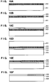
- Figs. 10A to 10F are views, respectively, showing the method of fabricating a semiconductor wafer.
- the first substrate is prepared by forming a porous silicon layer on a single-crystal silicon substrate, forming a non porous layer on the porous silicon layer, and preferably forming an insulating film on the non porous layer.
- the first structure and a second substrate prepared separately are so bonded as to sandwich the insulating film between them.
- the single-crystal silicon substrate is removed from the back surface of the first substrate, and the porous silicon layer is etched to fabricate a semiconductor substrate.
- a single-crystal Si substrate 501 for forming the first substrate is prepared, and a porous Si layer 502 is formed on the major surface of the single-crystal Si substrate 501 (Fig. 10A).
- At least one non porous layer 503 is formed on the porous Si layer 502 (Fig. 10B).
- Preferable examples of the non porous layer 503 are a single-crystal Si layer, a poly-Si layer, an amorphous Si layer, a metal film layer, a compound semiconductor layer, and a superconductor layer.
- An element such as MOSFET may be formed on the non porous layer 503.
- An SiO 2 layer 504 is preferably formed as another non porous layer on the non porous layer 503, and used as the first substrate (Fig. 10C).
- the SiO 2 layer 504 is useful because, when the first substrate and a second substrate 505 are bonded in the subsequent step, the interface energy at the bonded interface can be removed from an active layer.
- the first substrate and the second substrate 505 are tightly bonded at room temperature so as to sandwich the SiO 2 layer 504 between them (Fig. 10D).
- This bonding may be strengthened by performing anodic bonding, pressurization, or heat treatment, as needed, or a combination of them.
- the first substrate is preferably bonded to the second substrate 505 after the SiO 2 layer 504 is formed on the surface of the single-crystal Si layer by thermal oxidization or the like.
- the second substrate 505 are an Si substrate, a substrate having an SiO 2 layer formed on an Si substrate, a light-transmitting substrate such as a quartz substrate or the like, and a sapphire substrate.
- the second substrate 505 suffices to have a flat surface to be bonded, and may be another type of substrate.
- Fig. 10D shows the bonded state of the first and second substrates via the SiO 2 layer 504.
- the SiO 2 layer 504 need not be formed when the non porous layer 503 or the second substrate is not Si.
- a thin insulating plate may be inserted between the first and second substrates.
- the first substrate is removed from the second substrate at the boundary of the porous Si layer 502 (Fig. 10E).
- the removal method includes the first method (of discarding the first substrate) using grinding, polishing, etching, or the like, and the second method of separating the first and second substrates at the boundary of the porous layer 502.
- the first substrate can be recycled by removing porous Si left on the separated first substrate, and planarizing the surface of the first substrate, as needed.
- the porous Si layer 502 is selectively etched and removed (Fig. 10F).
- the wafer processing apparatus 100 is suitable for this etching. Since this wafer processing apparatus supplies ultrasonic waves while completely dipping a wafer (in this case, the wafer shown in Fig. 10E) into an etching solution and moving (e.g., rotating or vertically moving) it, the wafer is hardly contaminated by particles, and the etching is made uniform. According to this wafer processing apparatus, the etching time is shortened, and the etching selectivity between the non porous layer 503 and the porous layer 504 increases. The etching time is shortened because etching is promoted by ultrasonic waves, and the etching selectivity increases because the promotion of etching by ultrasonic waves is more remarkable on the porous layer 504 than on the non porous layer 503.
- the non porous layer 503 is single-crystal Si
- the following etching solutions are suited in addition to a general etching solution for Si.
- the porous layer 502 can be selectively etched to leave the underlying non porous layer 503 (single-crystal Si).
- the porous layer 502 is readily selectively etched by these etching solutions because porous Si has an enormous surface area and hence etching of the porous Si progresses at a very high speed in comparison with the non porous Si layer.
- Fig. 10E schematically shows a semiconductor substrate obtained by the above fabrication method.
- the flat non porous layer 503 e.g., single-crystal Si layer
- the flat non porous layer 503 is uniformly formed on the entire surface of the second substrate 505.
- the semiconductor substrate obtained by the above fabrication method is effectively used to form insulated electronic elements.
- This example is directed to cleaning processing.
- Wafers were set in the wafer processing bath 10 filled with ultrapure water, and ultrasonic waves of about 1 MHz were applied to clean the wafers while the wafers were rotated. By this cleaning, 90% or more of particles on the wafer surfaces were removed. Also, this removal of particles was done uniformly on the wafer surface.
- This example concerns cleaning processing using a solution mixture of ammonia, hydrogen peroxide, and ultrapure water. Cleaning using this solution mixture is suited to particle removal from the surface of a silicon wafer.
- Silicon wafers were set in the wafer processing bath 10 filled with a solution mixture of ammonia, hydrogen peroxide, and ultrapure water at about 80°C. While the wafers were rotated, ultrasonic waves of about 1 MHz were applied to clean the wafers. By this cleaning, 95% or more of particles were removed from the wafer surfaces. Also, this removal of particles was done uniformly on the wafer surface.
- This example pertains to etching of a silicon layer.
- Silicon wafers were set in the wafer processing bath 10 filled with a solution mixture prepared by mixing hydrofluoric acid, nitric acid, and acetic acid at a ratio of 1 : 200 : 200. While the wafers were rotated, ultrasonic waves of about 0.5 MHz were applied to etch the wafer surfaces for 30 sec. Consequently, the silicon wafers were uniformly etched by about 1.0 ⁇ m. The uniformity of the etching rate was ⁇ 5% or less on the wafer surface and between the wafers.
- This example relates to etching of an SiO 2 layer.
- Hydrofluoric acid is suitable for the etching of an SiO 2 layer.
- Wafers on which an SiO 2 layer was formed were set in the wafer processing bath 10 filled with 1.2% hydrofluoric acid. While the wafers were rotated, ultrasonic waves of about 0.5 MHz were applied to etch the SiO 2 layer for 30 sec. Consequently, the SiO 2 layer was uniformly etched by about 4 nm. The uniformity of the etching rate was ⁇ 3% or less on the wafer surface and between the wafers.
- Hot concentrated phosphoric acid is suitable for the etching of an Si 3 N 4 layer.
- Wafers on which an Si 3 N 4 layer was formed were set in the wafer processing bath 10 filled with hot concentrated phosphoric acid. While the wafers were rotated, ultrasonic waves of about 0.5 MHz were applied to etch the Si 3 N 4 layer. Consequently, the Si 3 N 4 layer was uniformly etched by about 100 nm. The uniformity of the etching rate was ⁇ 3% or less on the wafer surface and between the wafers.
- This example exemplifies to etching of a porous silicon layer.
- a solution mixture of hydrofluoric acid, hydrogen peroxide, and ultrapure water is suitable for the etching of a porous silicon layer.
- Wafers having a porous silicon layer were set in the wafer processing bath 10 filled with a solution mixture of hydrofluoric acid, hydrogen peroxide, and ultrapure water. While the wafers were rotated, ultrasonic waves of about 0.25 MHz were applied to etch the porous silicon layer. Consequently, the porous silicon layer was uniformly etched by 5 ⁇ m. The uniformity of the etching rate was ⁇ 3% or less on the wafer surface and between the wafers.
- porous silicon is etched when an etching solution penetrates into the pores of porous silicon by a capillary action and etches the walls of the pores. As the walls of the pores become thinner, these walls cannot support themselves beyond some point. Finally, the porous layer entirely collapses to complete the etching.
- FIGs. 10A to 10F are sectional views showing the steps of the SOI wafer fabrication method according to this example.
- a single-crystal Si substrate 501 for forming a first substrate was anodized in an HF solution to form a porous Si layer 502 (Fig. 10A).
- the anodization conditions were as follows.
- the resultant substrate was allowed to oxidize in an oxygen atmosphere at 400°C for 1 h.
- the inner walls of pores of the porous Si layer 502 were covered with a thermal oxide film.
- a 0.30- ⁇ m thick single-crystal Si layer 503 was epitaxially grown on the porous Si layer 502 by a CVD (Chemical Vapor Deposition) process (Fig. 10B).
- the epitaxial growth conditions were as follows.
- a 200-nm thick SiO 2 layer 504 was formed on the single-crystal Si layer (epitaxial layer) 503 by thermal oxidation (Fig. 10C).
- the first substrate thus formed as shown in Fig. 10C and an Si substrate 505 as a second substrate were so bonded as to sandwich the SiO 2 layer 504 (Fig. 10D).
- the single-crystal Si substrate 501 was removed from the first substrate to expose the porous Si layer 502 (Fig. 10E).
- the wafers shown in Fig. 10E were set in the wafer processing bath 10 filled with a solution mixture of hydrofluoric acid, hydrogen peroxide, and ultrapure water. While the wafers were rotated, ultrasonic waves of about 0.25 MHz were applied to etch the porous Si layer 502 (Fig. 10F). The uniformity of the etching rate of the porous Si layer 502 was ⁇ 5% or less on the wafer surface and between the wafers. By applying ultrasonic waves while wafers are rotated as described above, it is possible to uniformly promote the collapse (etching) of porous Si on the wafer surface and between the wafers.
- the single-crystal Si layer (epitaxial layer) 503 functions as an etching stop layer. Therefore, the porous Si layer 502 is selectively etched on the entire surface of the wafer.
- the rate at which the single-crystal Si layer 503 is etched by the etching solution described above is very low, so the etching selectivity of the porous Si layer 502 to the single-crystal Si layer 503 is 10 5 or more. Accordingly, the etching amount of the single-crystal Si layer 503 is about a few tens of ⁇ and practically negligible.
- Fig. 10F shows the SOI wafer obtained by the above steps.
- This SOI wafer has the 0.2- ⁇ m thick single-crystal Si layer 503 on the SiO 2 layer 504.
- the film thickness of this single-crystal Si layer 503 was measured at one hundred points over the entire surface and found to be 201 nm ⁇ 4 nm.
- a heat treatment was further performed in a hydrogen atmosphere at 1100°C for about 1 h.
- the surface roughness of the resultant SOI wafers was evaluated with an atomic force microscope (AFM), the root-mean-square of the surface roughness in a square region of 5 ⁇ m side was about 0.2 nm. This quality is equivalent to that of common Si wafers on the market.
- the heat treatment in the hydrogen atmosphere was performed at a temperature of 1,000°C or less in order to prevent slip in the single-crystal Si layer 503 caused by the difference between the thermal expansion coefficients of the quartz (second substrate) and the single-crystal Si layer 503.
- a single-crystal Si substrate 501 for forming a first substrate was anodized in an HF solution to form a porous Si layer 502 (Fig. 10A).
- the anodization conditions were as follows.
- the resultant substrate was allowed to oxidize in an oxygen atmosphere at 400°C for 1 h.
- the inner walls of pores of the porous Si layer 502 were covered with a thermal oxide film.
- a 0.15- ⁇ m thick single-crystal Si layer 503 was epitaxially grown on the porous Si layer 502 by a CVD (Chemical Vapor Deposition) process (Fig. 10B).
- the epitaxial growth conditions were as follows.
- a 100-nm thick SiO 2 layer 504 was formed on the single-crystal Si layer (epitaxial layer) 503 by oxidation (Fig. 10C).
- the first substrate thus formed as shown in Fig. 10C and a second Si substrate 505 were so bonded as to sandwich the SiO 2 layer 504 (Fig. 10D).
- the bonded wafers was separated into two wafers from the porous Si layer formed at a current density of 21 mA/cm 2 (second stage), thereby exposing the porous Si layer 503 to the surface of the second substrate 505 (Fig. 10E).
- Examples of the method of separating the bonded wafers are 1) mechanically pulling the two substrates, 2) twisting the substrates, 3) pressurizing the substrates, 4) driving a wedge between the substrates, 5) peeling the substrates by oxidizing from their end faces, 6) using thermal stress, and 7) applying ultrasonic waves, and it is possible to selectively use any of these methods.
- the wafers shown in Fig. 10E were set in the wafer processing bath 10 filled with a solution mixture of hydrofluoric acid, hydrogen peroxide, and ultrapure water. While the wafers were rotated, ultrasonic waves of about 0.25 MHz were applied to etch the porous Si layer 502 (Fig. 10F). The uniformity of the etching rate of the porous Si layer 502 was ⁇ 5% or less on the wafer surface and between the wafers. By applying ultrasonic waves while wafers are rotated as described above, it is possible to uniformly promote the collapse (etching) of porous Si on the wafer surface and between the wafers.
- the single-crystal Si layer (epitaxial layer) 503 functions as an etching stop layer. Therefore, the porous Si layer 502 is selectively etched on the entire surface of the wafer.
- the rate at which the single-crystal Si layer 503 is etched by the etching solution described above is very low, so the etching selectivity of the porous Si layer 502 to the single-crystal Si layer 503 is 10 5 or more. Accordingly, the etching amount of the single-crystal Si layer 503 is about a few tens of ⁇ and practically negligible.
- Fig. 10F shows the SOI wafer obtained by the above steps.
- This SOI wafer has the 0.1- ⁇ m thick single-crystal Si layer 503 on the SiO 2 layer 504.
- the film thickness of this single-crystal Si layer 503 was measured at one hundred points over the entire surface and found to be 101 nm ⁇ 3 nm.
- a heat treatment was further performed in a hydrogen atmosphere at 1,100°C for about 1 h.
- the surface roughness of the resultant SOI wafers was evaluated with an atomic force microscope (AFM)
- the root-mean-square of the surface roughness in a square region of 5 ⁇ m side was about 0.2 nm. This quality is equivalent to that of common Si wafers on the market.
- the heat treatment in the hydrogen atmosphere was performed at a temperature of 1,000°C or less in order to prevent slip in the single-crystal Si layer 503 caused by the difference between the thermal expansion coefficients of the quartz (second substrate) and the single-crystal Si layer 503.
- the first substrate obtained by separating the bonded wafers into two wafers can be reused. That is, the separated substrate can be reused as the first or second substrate by selectively etching the porous Si film remaining on the surface of the substrate by the same etching method as for the porous Si film described above and processing the resultant material (e.g., annealing in a hydrogen processing or a surface treatment such as surface polishing).
- epitaxial growth is used to form a single-crystal Si layer on a porous Si layer.
- various methods such as CVD, MBE, sputtering, and liquid phase growth in the formation of a single-crystal Si layer.
- a semiconductor layer of a single-crystal compound such as GaAs or InP can be formed on a porous Si layer by epitaxial growth. If this is the case, wafers suited to high-frequency devices such as "GaAs on Si” and “GaAs on Glass (Quartz)" and OEIC can be made.
- the present invention can reduce contamination of wafers by particles and make wafer processing uniform.
- An ultrasonic bath (30) is arranged below a wafer processing bath (10). Wafers (40) are processed while ultrasonic waves are transmitted from the ultrasonic bath (30) to the wafer processing bath (10). The wafers (40) are processed while being entirely dipped into the wafer processing bath (10) and rotated by wafer rotating rods (53).
Landscapes
- Engineering & Computer Science (AREA)
- Microelectronics & Electronic Packaging (AREA)
- Condensed Matter Physics & Semiconductors (AREA)
- General Physics & Mathematics (AREA)
- Manufacturing & Machinery (AREA)
- Computer Hardware Design (AREA)
- Physics & Mathematics (AREA)
- Power Engineering (AREA)
- Chemical & Material Sciences (AREA)
- Chemical Kinetics & Catalysis (AREA)
- General Chemical & Material Sciences (AREA)
- Weting (AREA)
- Cleaning Or Drying Semiconductors (AREA)
Applications Claiming Priority (6)
| Application Number | Priority Date | Filing Date | Title |
|---|---|---|---|
| JP38080/97 | 1997-02-21 | ||
| JP03808097A JP3831878B2 (ja) | 1997-02-21 | 1997-02-21 | ウェハ処理装置 |
| JP3807997 | 1997-02-21 | ||
| JP3808097 | 1997-02-21 | ||
| JP03807997A JP3831877B2 (ja) | 1997-02-21 | 1997-02-21 | 半導体基体の製造方法 |
| JP38079/97 | 1997-02-21 |
Publications (2)
| Publication Number | Publication Date |
|---|---|
| EP0860860A2 true EP0860860A2 (de) | 1998-08-26 |
| EP0860860A3 EP0860860A3 (de) | 2001-11-28 |
Family
ID=26377262
Family Applications (1)
| Application Number | Title | Priority Date | Filing Date |
|---|---|---|---|
| EP98102897A Withdrawn EP0860860A3 (de) | 1997-02-21 | 1998-02-19 | Vorrichtung zum Behandeln von Wafern, Verfahren zum Behandeln von Wafern und Verfahren zur Herstellung eines Halbleitersubstrats |
Country Status (8)
| Country | Link |
|---|---|
| US (1) | US6199563B1 (de) |
| EP (1) | EP0860860A3 (de) |
| KR (2) | KR100306054B1 (de) |
| CN (1) | CN1111900C (de) |
| AU (1) | AU742258B2 (de) |
| CA (1) | CA2229975C (de) |
| SG (1) | SG63810A1 (de) |
| TW (1) | TW504041U (de) |
Cited By (12)
| Publication number | Priority date | Publication date | Assignee | Title |
|---|---|---|---|---|
| EP0856873A2 (de) * | 1997-02-04 | 1998-08-05 | Canon Kabushiki Kaisha | Vorrichtung und Methode zur Behandlung von Halbleiter-Plättchen und SOI Halbleiterscheibe Herstellungsverfahren |
| WO1999026276A1 (en) * | 1997-11-13 | 1999-05-27 | Memc Electronic Materials, Inc. | Apparatus for cleaning semiconductor wafers |
| EP0936663A2 (de) * | 1998-01-14 | 1999-08-18 | Canon Kabushiki Kaisha | Verfahren zur Entfernung eines porösen Bereiches und Verfahren zur Herstellung eines Halbleiter-Substrates |
| US6119708A (en) * | 1998-11-11 | 2000-09-19 | Applied Materials, Inc. | Method and apparatus for cleaning the edge of a thin disc |
| BE1013029A3 (nl) * | 1999-02-19 | 2001-08-07 | Ultra Clean Bv Met Beperkte Aa | Ultrasoon reinigingsinrichting. |
| US6391067B2 (en) | 1997-02-04 | 2002-05-21 | Canon Kabushiki Kaisha | Wafer processing apparatus and method, wafer convey robot, semiconductor substrate fabrication method, and semiconductor fabrication apparatus |
| US6410436B2 (en) | 1999-03-26 | 2002-06-25 | Canon Kabushiki Kaisha | Method of cleaning porous body, and process for producing porous body, non-porous film or bonded substrate |
| US6436302B1 (en) | 1999-08-23 | 2002-08-20 | Applied Materials, Inc. | Post CU CMP polishing for reduced defects |
| US6572453B1 (en) | 1998-09-29 | 2003-06-03 | Applied Materials, Inc. | Multi-fluid polishing process |
| US7220322B1 (en) | 2000-08-24 | 2007-05-22 | Applied Materials, Inc. | Cu CMP polishing pad cleaning |
| WO2008133593A2 (en) * | 2007-04-27 | 2008-11-06 | Jcs-Echigo Pte Ltd | Cleaning process and apparatus |
| CN106824884A (zh) * | 2017-03-31 | 2017-06-13 | 贵州大学 | 一种硅片翻转冲洗装置 |
Families Citing this family (45)
| Publication number | Priority date | Publication date | Assignee | Title |
|---|---|---|---|---|
| KR20000067106A (ko) * | 1999-04-23 | 2000-11-15 | 구본준 | 유리기판 에칭장치 |
| JP3111979B2 (ja) * | 1998-05-20 | 2000-11-27 | 日本電気株式会社 | ウエハの洗浄方法 |
| US6732749B2 (en) * | 2000-12-22 | 2004-05-11 | Akrion, Llc | Particle barrier drain |
| US6448096B1 (en) * | 2001-05-23 | 2002-09-10 | Advanced Micro Devices, Inc. | Atomic force microscopy and signal acquisition via buried insulator |
| AU2002339592A1 (en) * | 2001-10-29 | 2003-05-12 | Analog Devices Inc. | A method for bonding a pair of silicon wafers together and a semiconductor wafer |
| US20030181042A1 (en) * | 2002-03-19 | 2003-09-25 | Taiwan Semiconductor Manufacturing Co., Ltd. | Etching uniformity in wet bench tools |
| US7185661B2 (en) * | 2002-05-06 | 2007-03-06 | Akrion Technologies, Inc. | Reciprocating megasonic probe |
| US20030211427A1 (en) * | 2002-05-07 | 2003-11-13 | Taiwan Semiconductor Manufacturing Co., Ltd. | Method and apparatus for thick film photoresist stripping |
| KR20040000754A (ko) * | 2002-06-25 | 2004-01-07 | 동부전자 주식회사 | 반도체 웨이퍼 세정장치 |
| US20040072448A1 (en) * | 2002-10-15 | 2004-04-15 | Brask Justin K. | Protecting delicate semiconductor features during wet etching |
| US20040077172A1 (en) * | 2002-10-17 | 2004-04-22 | Brask Justin K | Wet etching narrow trenches |
| JP4509501B2 (ja) * | 2003-07-31 | 2010-07-21 | Sumco Techxiv株式会社 | 円板状部材のエッチング方法及び装置 |
| US7754609B1 (en) * | 2003-10-28 | 2010-07-13 | Applied Materials, Inc. | Cleaning processes for silicon carbide materials |
| US20050132332A1 (en) * | 2003-12-12 | 2005-06-16 | Abhay Sathe | Multi-location coordinated test apparatus |
| US20050211379A1 (en) * | 2004-03-29 | 2005-09-29 | Hung-Wen Su | Apparatus and method for removing metal from wafer edge |
| JP2006108512A (ja) * | 2004-10-07 | 2006-04-20 | Ses Co Ltd | 基板処理装置 |
| KR100687296B1 (ko) * | 2005-12-27 | 2007-02-27 | 한국기계연구원 | 자전형 웨이퍼 캐리어와 이를 구비한 초음파 세정장치 |
| KR100939612B1 (ko) * | 2005-12-29 | 2010-02-01 | 엘지디스플레이 주식회사 | 배향막의 러빙장치 |
| JP4762822B2 (ja) | 2006-08-03 | 2011-08-31 | 東京エレクトロン株式会社 | 薬液混合方法および薬液混合装置 |
| US7789969B2 (en) * | 2006-11-01 | 2010-09-07 | Applied Materials, Inc. | Methods and apparatus for cleaning chamber components |
| JP4451430B2 (ja) * | 2006-11-28 | 2010-04-14 | 昭和電工株式会社 | 磁気記録媒体用基板の洗浄装置および洗浄方法 |
| KR20120081513A (ko) * | 2011-01-11 | 2012-07-19 | 삼성모바일디스플레이주식회사 | 마스크 세정 장치 |
| CN102247928A (zh) * | 2011-05-11 | 2011-11-23 | 江西旭阳雷迪高科技股份有限公司 | 一种过滤装置及其过滤工艺 |
| DE102012214316A1 (de) * | 2012-08-10 | 2014-02-13 | Siltronic Ag | Halterung für eine Vielzahl von scheibenförmigen Werkstücken |
| CN104690030A (zh) * | 2013-12-05 | 2015-06-10 | 天津中环领先材料技术有限公司 | 一种改造后的硅片清洗机用槽体 |
| CN104971921A (zh) * | 2014-04-08 | 2015-10-14 | 麒麟电子(深圳)有限公司 | 玻璃基板清洗装置 |
| CN105057273A (zh) * | 2015-08-27 | 2015-11-18 | 苏州凯锝微电子有限公司 | 一种超声波镜片清洗装置 |
| US9704820B1 (en) * | 2016-02-26 | 2017-07-11 | Taiwan Semiconductor Manufacturing Company Ltd. | Semiconductor manufacturing method and associated semiconductor manufacturing system |
| CN106115715A (zh) * | 2016-06-26 | 2016-11-16 | 河南盛达光伏科技有限公司 | 多晶硅铸锭半融工艺产生的循环尾料清洗处理方法 |
| CN106925565B (zh) * | 2017-02-09 | 2018-08-24 | 同济大学 | 一种lbo晶体的刻蚀清洗方法 |
| CN107968060B (zh) * | 2017-11-21 | 2020-05-12 | 长江存储科技有限责任公司 | 用于晶圆刻蚀的反应槽 |
| CN107946229B (zh) * | 2017-11-21 | 2021-01-26 | 长江存储科技有限责任公司 | 用于晶圆刻蚀的升降装置 |
| CN108480305A (zh) * | 2018-04-12 | 2018-09-04 | 绍兴文理学院 | 一种光伏硅片清洗设备 |
| CN109371456B (zh) * | 2018-10-17 | 2021-01-08 | 山东博达光电有限公司 | 人造石英晶体籽晶片的腐蚀装置及腐蚀方法 |
| US20200307523A1 (en) * | 2018-10-19 | 2020-10-01 | Lg Electronics Inc. | Vehicle optical device |
| CN109604251B (zh) * | 2018-12-29 | 2022-04-05 | 西安奕斯伟材料科技有限公司 | 一种清洗装置及清洗方法 |
| CN109759937A (zh) * | 2019-01-30 | 2019-05-17 | 西安奕斯伟硅片技术有限公司 | 一种硅片的处理方法和装置 |
| CN110369390A (zh) * | 2019-07-05 | 2019-10-25 | 上海提牛机电设备有限公司 | 一种陶瓷盘360度旋装置 |
| CN110739247A (zh) * | 2019-09-19 | 2020-01-31 | 上海提牛机电设备有限公司 | 一种晶圆蚀刻槽 |
| CN110660662B (zh) * | 2019-10-08 | 2021-02-02 | 江苏晟驰微电子有限公司 | 一种新型硅腐蚀工艺 |
| CN110813888A (zh) * | 2019-10-30 | 2020-02-21 | 苏州晶洲装备科技有限公司 | 一种掩模版清洗装置和掩模版清洗方法 |
| JP7381370B2 (ja) * | 2020-03-05 | 2023-11-15 | キオクシア株式会社 | 半導体製造装置および半導体装置の製造方法 |
| TWI744988B (zh) * | 2020-07-17 | 2021-11-01 | 禾邑實業股份有限公司 | 清洗及蝕刻裝置 |
| CN112371619B (zh) * | 2020-10-22 | 2022-04-05 | 华帝股份有限公司 | 用于烹饪设备的清洁控制方法及应用其的烹饪设备 |
| CN115156182B (zh) * | 2022-07-01 | 2023-05-16 | 青岛凯瑞电子有限公司 | 一种镀镍用超声波清洗装置 |
Citations (12)
| Publication number | Priority date | Publication date | Assignee | Title |
|---|---|---|---|---|
| US2702260A (en) * | 1949-11-17 | 1955-02-15 | Massa Frank | Apparatus and method for the generation and use of sound waves in liquids for the high-speed wetting of substances immersed in the liquid |
| US4191295A (en) * | 1978-08-14 | 1980-03-04 | Rca Corporation | Processing rack |
| EP0319806A1 (de) * | 1987-11-28 | 1989-06-14 | Kabushiki Kaisha Toshiba | Verfahren zur Obenflächenbehandlung eines Halbleiterplättchens |
| FR2626261A1 (fr) * | 1988-01-26 | 1989-07-28 | Recif Sa | Appareil elevateur de plaquettes de silicium notamment |
| US4854337A (en) * | 1988-05-24 | 1989-08-08 | Eastman Kodak Company | Apparatus for treating wafers utilizing megasonic energy |
| JPH01304733A (ja) * | 1988-06-01 | 1989-12-08 | Mitsubishi Electric Corp | 半導体ウエハの洗浄装置 |
| JPH03257826A (ja) * | 1990-03-07 | 1991-11-18 | Shimada Phys & Chem Ind Co Ltd | 半導体ウェハの洗浄方法 |
| EP0554795A1 (de) * | 1992-01-31 | 1993-08-11 | Canon Kabushiki Kaisha | Substrat für eine Halbleitervorrichtung und Verfahren zur Vorbereitung desselben |
| US5327921A (en) * | 1992-03-05 | 1994-07-12 | Tokyo Electron Limited | Processing vessel for a wafer washing system |
| EP0694957A1 (de) * | 1994-07-29 | 1996-01-31 | Co.Ri.M.Me. Consorzio Per La Ricerca Sulla Microelettronica Nel Mezzogiorno | Gerät für die Behandlung von Halbleiterscheiben mit Flüssigkeiten |
| EP0740331A2 (de) * | 1995-04-19 | 1996-10-30 | MEMC Electronic Materials, Inc. | Verfahren zur Reinigung von halbleitenden Wafern und Einrichtung dafür |
| JPH08316182A (ja) * | 1995-05-12 | 1996-11-29 | Tokyo Electron Ltd | 処理装置 |
Family Cites Families (21)
| Publication number | Priority date | Publication date | Assignee | Title |
|---|---|---|---|---|
| US3964957A (en) * | 1973-12-19 | 1976-06-22 | Monsanto Company | Apparatus for processing semiconductor wafers |
| JPS53144265A (en) * | 1977-05-23 | 1978-12-15 | Hitachi Ltd | Etching device |
| US4325394A (en) * | 1980-08-25 | 1982-04-20 | Micro Air Systems, Inc. | Submersible motor chemical processing apparatus |
| US4736760A (en) | 1986-02-21 | 1988-04-12 | Robert A. Coberly | Apparatus for cleaning, rinsing and drying substrates |
| JPS62283632A (ja) * | 1986-05-31 | 1987-12-09 | Toshiba Corp | ウエハ処理装置 |
| US4804007A (en) | 1987-04-29 | 1989-02-14 | Verteq, Inc. | Cleaning apparatus |
| JPH01187931A (ja) * | 1988-01-22 | 1989-07-27 | Nec Yamagata Ltd | 半導体装置の製造方法 |
| JPH03121925A (ja) * | 1989-10-06 | 1991-05-23 | Suzuki Motor Corp | 車両のドア開閉構造 |
| US5090432A (en) * | 1990-10-16 | 1992-02-25 | Verteq, Inc. | Single wafer megasonic semiconductor wafer processing system |
| JPH05243203A (ja) | 1992-02-28 | 1993-09-21 | Fujitsu Ltd | 超音波洗浄装置 |
| JP3257826B2 (ja) * | 1992-06-30 | 2002-02-18 | 株式会社リコー | 画像処理装置 |
| JPH07142439A (ja) | 1993-11-12 | 1995-06-02 | Tokyo Ohka Kogyo Co Ltd | 半導体ウェーハの洗浄装置及び洗浄方法 |
| US5672212A (en) * | 1994-07-01 | 1997-09-30 | Texas Instruments Incorporated | Rotational megasonic cleaner/etcher for wafers |
| US5534106A (en) | 1994-07-26 | 1996-07-09 | Kabushiki Kaisha Toshiba | Apparatus for processing semiconductor wafers |
| JPH08117702A (ja) | 1994-10-19 | 1996-05-14 | Hitachi Ltd | ワーク処理方法および装置 |
| JPH0938079A (ja) | 1995-07-26 | 1997-02-10 | Toshiba Medical Eng Co Ltd | 超音波診断装置 |
| JPH0938080A (ja) | 1995-08-01 | 1997-02-10 | Matsushita Electric Ind Co Ltd | 超音波診断装置 |
| JP3050524B2 (ja) * | 1996-05-09 | 2000-06-12 | スピードファムクリーンシステム株式会社 | ワーク搬送用キャリヤ装置 |
| JP3623315B2 (ja) * | 1996-06-06 | 2005-02-23 | 信越半導体株式会社 | 円形薄板状物の支持治具 |
| JPH102889A (ja) * | 1996-06-14 | 1998-01-06 | Nippon Soken Inc | 材料評価装置 |
| US5816274A (en) * | 1997-04-10 | 1998-10-06 | Memc Electronic Materials, Inc. | Apparartus for cleaning semiconductor wafers |
-
1998
- 1998-02-10 TW TW090218651U patent/TW504041U/zh unknown
- 1998-02-10 SG SG1998000290A patent/SG63810A1/en unknown
- 1998-02-18 US US09/025,409 patent/US6199563B1/en not_active Expired - Lifetime
- 1998-02-18 AU AU55370/98A patent/AU742258B2/en not_active Ceased
- 1998-02-18 CA CA002229975A patent/CA2229975C/en not_active Expired - Fee Related
- 1998-02-19 EP EP98102897A patent/EP0860860A3/de not_active Withdrawn
- 1998-02-20 KR KR1019980005354A patent/KR100306054B1/ko not_active IP Right Cessation
- 1998-02-20 CN CN98105320A patent/CN1111900C/zh not_active Expired - Fee Related
-
2000
- 2000-11-04 KR KR1020000065431A patent/KR100347824B1/ko not_active IP Right Cessation
Patent Citations (12)
| Publication number | Priority date | Publication date | Assignee | Title |
|---|---|---|---|---|
| US2702260A (en) * | 1949-11-17 | 1955-02-15 | Massa Frank | Apparatus and method for the generation and use of sound waves in liquids for the high-speed wetting of substances immersed in the liquid |
| US4191295A (en) * | 1978-08-14 | 1980-03-04 | Rca Corporation | Processing rack |
| EP0319806A1 (de) * | 1987-11-28 | 1989-06-14 | Kabushiki Kaisha Toshiba | Verfahren zur Obenflächenbehandlung eines Halbleiterplättchens |
| FR2626261A1 (fr) * | 1988-01-26 | 1989-07-28 | Recif Sa | Appareil elevateur de plaquettes de silicium notamment |
| US4854337A (en) * | 1988-05-24 | 1989-08-08 | Eastman Kodak Company | Apparatus for treating wafers utilizing megasonic energy |
| JPH01304733A (ja) * | 1988-06-01 | 1989-12-08 | Mitsubishi Electric Corp | 半導体ウエハの洗浄装置 |
| JPH03257826A (ja) * | 1990-03-07 | 1991-11-18 | Shimada Phys & Chem Ind Co Ltd | 半導体ウェハの洗浄方法 |
| EP0554795A1 (de) * | 1992-01-31 | 1993-08-11 | Canon Kabushiki Kaisha | Substrat für eine Halbleitervorrichtung und Verfahren zur Vorbereitung desselben |
| US5327921A (en) * | 1992-03-05 | 1994-07-12 | Tokyo Electron Limited | Processing vessel for a wafer washing system |
| EP0694957A1 (de) * | 1994-07-29 | 1996-01-31 | Co.Ri.M.Me. Consorzio Per La Ricerca Sulla Microelettronica Nel Mezzogiorno | Gerät für die Behandlung von Halbleiterscheiben mit Flüssigkeiten |
| EP0740331A2 (de) * | 1995-04-19 | 1996-10-30 | MEMC Electronic Materials, Inc. | Verfahren zur Reinigung von halbleitenden Wafern und Einrichtung dafür |
| JPH08316182A (ja) * | 1995-05-12 | 1996-11-29 | Tokyo Electron Ltd | 処理装置 |
Non-Patent Citations (4)
| Title |
|---|
| PATENT ABSTRACTS OF JAPAN vol. 014, no. 102 (E-0894), 23 February 1990 (1990-02-23) & JP 01 304733 A (MITSUBISHI ELECTRIC CORP), 8 December 1989 (1989-12-08) * |
| PATENT ABSTRACTS OF JAPAN vol. 016, no. 059 (E-1166), 14 February 1992 (1992-02-14) & JP 03 257826 A (SHIMADA PHYS & CHEM IND CO LTD;OTHERS: 01), 18 November 1991 (1991-11-18) * |
| PATENT ABSTRACTS OF JAPAN vol. 1997, no. 03, 31 March 1997 (1997-03-31) & JP 08 316182 A (TOKYO ELECTRON LTD;TOKYO ELECTRON KYUSHU KK), 29 November 1996 (1996-11-29) * |
| SAKAGUCHI K ET AL: "EXTREMELY HIGH SELECTIVE ETCHING OF POROUS SI FOR SINGLE ETCH-STOP BOND-AND-ETCH-BACK SILICON-ON-INSULATOR" JAPANESE JOURNAL OF APPLIED PHYSICS,PUBLICATION OFFICE JAPANESE JOURNAL OF APPLIED PHYSICS. TOKYO,JP, vol. 34, no. PART 01, 02B, 1995, pages 842-847, XP000199399 ISSN: 0021-4922 * |
Cited By (18)
| Publication number | Priority date | Publication date | Assignee | Title |
|---|---|---|---|---|
| EP0856873A2 (de) * | 1997-02-04 | 1998-08-05 | Canon Kabushiki Kaisha | Vorrichtung und Methode zur Behandlung von Halbleiter-Plättchen und SOI Halbleiterscheibe Herstellungsverfahren |
| US6391067B2 (en) | 1997-02-04 | 2002-05-21 | Canon Kabushiki Kaisha | Wafer processing apparatus and method, wafer convey robot, semiconductor substrate fabrication method, and semiconductor fabrication apparatus |
| EP0856873A3 (de) * | 1997-02-04 | 2001-08-29 | Canon Kabushiki Kaisha | Vorrichtung und Methode zur Behandlung von Halbleiter-Plättchen und SOI Halbleiterscheibe Herstellungsverfahren |
| US6337030B1 (en) | 1997-02-04 | 2002-01-08 | Canon Kabushiki Kaisha | Wafer processing apparatus, wafer processing method, and SOI wafer fabrication method |
| WO1999026276A1 (en) * | 1997-11-13 | 1999-05-27 | Memc Electronic Materials, Inc. | Apparatus for cleaning semiconductor wafers |
| US6380099B2 (en) | 1998-01-14 | 2002-04-30 | Canon Kabushiki Kaisha | Porous region removing method and semiconductor substrate manufacturing method |
| EP0936663A2 (de) * | 1998-01-14 | 1999-08-18 | Canon Kabushiki Kaisha | Verfahren zur Entfernung eines porösen Bereiches und Verfahren zur Herstellung eines Halbleiter-Substrates |
| EP0936663A3 (de) * | 1998-01-14 | 1999-09-08 | Canon Kabushiki Kaisha | Verfahren zur Entfernung eines porösen Bereiches und Verfahren zur Herstellung eines Halbleiter-Substrates |
| US6572453B1 (en) | 1998-09-29 | 2003-06-03 | Applied Materials, Inc. | Multi-fluid polishing process |
| US6119708A (en) * | 1998-11-11 | 2000-09-19 | Applied Materials, Inc. | Method and apparatus for cleaning the edge of a thin disc |
| US6276371B1 (en) * | 1998-11-11 | 2001-08-21 | Applied Materials, Inc. | Method and apparatus for cleaning the edge of a thin disc |
| BE1013029A3 (nl) * | 1999-02-19 | 2001-08-07 | Ultra Clean Bv Met Beperkte Aa | Ultrasoon reinigingsinrichting. |
| US6410436B2 (en) | 1999-03-26 | 2002-06-25 | Canon Kabushiki Kaisha | Method of cleaning porous body, and process for producing porous body, non-porous film or bonded substrate |
| US6436302B1 (en) | 1999-08-23 | 2002-08-20 | Applied Materials, Inc. | Post CU CMP polishing for reduced defects |
| US7220322B1 (en) | 2000-08-24 | 2007-05-22 | Applied Materials, Inc. | Cu CMP polishing pad cleaning |
| WO2008133593A2 (en) * | 2007-04-27 | 2008-11-06 | Jcs-Echigo Pte Ltd | Cleaning process and apparatus |
| WO2008133593A3 (en) * | 2007-04-27 | 2009-11-19 | Jcs-Echigo Pte Ltd | Cleaning process and apparatus |
| CN106824884A (zh) * | 2017-03-31 | 2017-06-13 | 贵州大学 | 一种硅片翻转冲洗装置 |
Also Published As
| Publication number | Publication date |
|---|---|
| AU742258B2 (en) | 2001-12-20 |
| TW504041U (en) | 2002-09-21 |
| CA2229975C (en) | 2003-02-18 |
| CN1191385A (zh) | 1998-08-26 |
| EP0860860A3 (de) | 2001-11-28 |
| KR100347824B1 (ko) | 2002-08-07 |
| KR19980071560A (ko) | 1998-10-26 |
| KR100306054B1 (ko) | 2001-11-02 |
| CN1111900C (zh) | 2003-06-18 |
| AU5537098A (en) | 1998-08-27 |
| SG63810A1 (en) | 1999-03-30 |
| CA2229975A1 (en) | 1998-08-21 |
| US6199563B1 (en) | 2001-03-13 |
Similar Documents
| Publication | Publication Date | Title |
|---|---|---|
| US6199563B1 (en) | Wafer processing apparatus, wafer processing method, and semiconductor substrate fabrication method | |
| EP0856873B1 (de) | Vorrichtung und Verfahren zur Behandlung von Halbleiter-Plättchen | |
| US6767840B1 (en) | Wafer processing apparatus, wafer processing method, and semiconductor substrate fabrication method | |
| JP3218564B2 (ja) | 多孔質領域の除去方法及び半導体基体の製造方法 | |
| US6180497B1 (en) | Method for producing semiconductor base members | |
| EP0940483A2 (de) | Anodisierungsverfahren und Vorrichtung und Verfahren zur Herstellung eines Halbleitersubstrats | |
| EP0938132B1 (de) | Verfahren zur Entfernung einer porösen Halbleiterzone und Verfahren zur Herstellung eines halbleitenden Substrats | |
| CA2228552C (en) | Wafer processing apparatus and method, wafer convey robot, semiconductor substrate fabrication method, and semiconductor fabrication apparatus | |
| JP3831878B2 (ja) | ウェハ処理装置 | |
| JP3831877B2 (ja) | 半導体基体の製造方法 | |
| JP2000133558A (ja) | 半導体基体の作製方法およびそれにより作製された基体 | |
| JP2004158882A (ja) | 半導体基体の製造方法 |
Legal Events
| Date | Code | Title | Description |
|---|---|---|---|
| PUAI | Public reference made under article 153(3) epc to a published international application that has entered the european phase |
Free format text: ORIGINAL CODE: 0009012 |
|
| AK | Designated contracting states |
Kind code of ref document: A2 Designated state(s): AT BE CH DE DK ES FI FR GB GR IE IT LI LU MC NL PT SE Kind code of ref document: A2 Designated state(s): AT BE CH DE ES FR GB IT LI NL PT SE |
|
| AX | Request for extension of the european patent |
Free format text: AL;LT;LV;MK;RO;SI |
|
| PUAL | Search report despatched |
Free format text: ORIGINAL CODE: 0009013 |
|
| AK | Designated contracting states |
Kind code of ref document: A3 Designated state(s): AT BE CH DE DK ES FI FR GB GR IE IT LI LU MC NL PT SE |
|
| AX | Request for extension of the european patent |
Free format text: AL;LT;LV;MK;RO;SI |
|
| 17P | Request for examination filed |
Effective date: 20020409 |
|
| AKX | Designation fees paid |
Free format text: AT BE CH DE ES FR GB IT LI NL PT SE |
|
| 17Q | First examination report despatched |
Effective date: 20041130 |
|
| STAA | Information on the status of an ep patent application or granted ep patent |
Free format text: STATUS: THE APPLICATION IS DEEMED TO BE WITHDRAWN |
|
| 18D | Application deemed to be withdrawn |
Effective date: 20050412 |