EP0860726A1 - Spitze Sonde mit Mikroöffnung zur Wahrnehmung oder Abstrahlung von Licht, optisches Nahfeldmikroskop, Aufzeichnungs- und Wiedergabegerät sowie Belichtungsgerät unter Verwendung dieser Sonde und Herstellungsverfahren der Sonde - Google Patents
Spitze Sonde mit Mikroöffnung zur Wahrnehmung oder Abstrahlung von Licht, optisches Nahfeldmikroskop, Aufzeichnungs- und Wiedergabegerät sowie Belichtungsgerät unter Verwendung dieser Sonde und Herstellungsverfahren der Sonde Download PDFInfo
- Publication number
- EP0860726A1 EP0860726A1 EP98102899A EP98102899A EP0860726A1 EP 0860726 A1 EP0860726 A1 EP 0860726A1 EP 98102899 A EP98102899 A EP 98102899A EP 98102899 A EP98102899 A EP 98102899A EP 0860726 A1 EP0860726 A1 EP 0860726A1
- Authority
- EP
- European Patent Office
- Prior art keywords
- light
- tip
- probe
- substrate
- layer
- Prior art date
- Legal status (The legal status is an assumption and is not a legal conclusion. Google has not performed a legal analysis and makes no representation as to the accuracy of the status listed.)
- Withdrawn
Links
Images


Classifications
-
- G—PHYSICS
- G01—MEASURING; TESTING
- G01Q—SCANNING-PROBE TECHNIQUES OR APPARATUS; APPLICATIONS OF SCANNING-PROBE TECHNIQUES, e.g. SCANNING PROBE MICROSCOPY [SPM]
- G01Q60/00—Particular types of SPM [Scanning Probe Microscopy] or microscopes; Essential components thereof
- G01Q60/18—SNOM [Scanning Near-Field Optical Microscopy] or apparatus therefor, e.g. SNOM probes
- G01Q60/22—Probes, their manufacture, or their related instrumentation, e.g. holders
-
- G—PHYSICS
- G03—PHOTOGRAPHY; CINEMATOGRAPHY; ANALOGOUS TECHNIQUES USING WAVES OTHER THAN OPTICAL WAVES; ELECTROGRAPHY; HOLOGRAPHY
- G03F—PHOTOMECHANICAL PRODUCTION OF TEXTURED OR PATTERNED SURFACES, e.g. FOR PRINTING, FOR PROCESSING OF SEMICONDUCTOR DEVICES; MATERIALS THEREFOR; ORIGINALS THEREFOR; APPARATUS SPECIALLY ADAPTED THEREFOR
- G03F7/00—Photomechanical, e.g. photolithographic, production of textured or patterned surfaces, e.g. printing surfaces; Materials therefor, e.g. comprising photoresists; Apparatus specially adapted therefor
- G03F7/70—Microphotolithographic exposure; Apparatus therefor
- G03F7/70375—Multiphoton lithography or multiphoton photopolymerization; Imaging systems comprising means for converting one type of radiation into another type of radiation
-
- G—PHYSICS
- G03—PHOTOGRAPHY; CINEMATOGRAPHY; ANALOGOUS TECHNIQUES USING WAVES OTHER THAN OPTICAL WAVES; ELECTROGRAPHY; HOLOGRAPHY
- G03F—PHOTOMECHANICAL PRODUCTION OF TEXTURED OR PATTERNED SURFACES, e.g. FOR PRINTING, FOR PROCESSING OF SEMICONDUCTOR DEVICES; MATERIALS THEREFOR; ORIGINALS THEREFOR; APPARATUS SPECIALLY ADAPTED THEREFOR
- G03F7/00—Photomechanical, e.g. photolithographic, production of textured or patterned surfaces, e.g. printing surfaces; Materials therefor, e.g. comprising photoresists; Apparatus specially adapted therefor
- G03F7/70—Microphotolithographic exposure; Apparatus therefor
- G03F7/70483—Information management; Active and passive control; Testing; Wafer monitoring, e.g. pattern monitoring
- G03F7/70605—Workpiece metrology
- G03F7/70616—Monitoring the printed patterns
-
- G—PHYSICS
- G11—INFORMATION STORAGE
- G11B—INFORMATION STORAGE BASED ON RELATIVE MOVEMENT BETWEEN RECORD CARRIER AND TRANSDUCER
- G11B7/00—Recording or reproducing by optical means, e.g. recording using a thermal beam of optical radiation by modifying optical properties or the physical structure, reproducing using an optical beam at lower power by sensing optical properties; Record carriers therefor
- G11B7/12—Heads, e.g. forming of the optical beam spot or modulation of the optical beam
- G11B7/122—Flying-type heads, e.g. analogous to Winchester type in magnetic recording
-
- G—PHYSICS
- G11—INFORMATION STORAGE
- G11B—INFORMATION STORAGE BASED ON RELATIVE MOVEMENT BETWEEN RECORD CARRIER AND TRANSDUCER
- G11B7/00—Recording or reproducing by optical means, e.g. recording using a thermal beam of optical radiation by modifying optical properties or the physical structure, reproducing using an optical beam at lower power by sensing optical properties; Record carriers therefor
- G11B7/12—Heads, e.g. forming of the optical beam spot or modulation of the optical beam
- G11B7/22—Apparatus or processes for the manufacture of optical heads, e.g. assembly
-
- G—PHYSICS
- G01—MEASURING; TESTING
- G01Q—SCANNING-PROBE TECHNIQUES OR APPARATUS; APPLICATIONS OF SCANNING-PROBE TECHNIQUES, e.g. SCANNING PROBE MICROSCOPY [SPM]
- G01Q80/00—Applications, other than SPM, of scanning-probe techniques
-
- Y—GENERAL TAGGING OF NEW TECHNOLOGICAL DEVELOPMENTS; GENERAL TAGGING OF CROSS-SECTIONAL TECHNOLOGIES SPANNING OVER SEVERAL SECTIONS OF THE IPC; TECHNICAL SUBJECTS COVERED BY FORMER USPC CROSS-REFERENCE ART COLLECTIONS [XRACs] AND DIGESTS
- Y10—TECHNICAL SUBJECTS COVERED BY FORMER USPC
- Y10S—TECHNICAL SUBJECTS COVERED BY FORMER USPC CROSS-REFERENCE ART COLLECTIONS [XRACs] AND DIGESTS
- Y10S977/00—Nanotechnology
- Y10S977/84—Manufacture, treatment, or detection of nanostructure
- Y10S977/849—Manufacture, treatment, or detection of nanostructure with scanning probe
- Y10S977/86—Scanning probe structure
- Y10S977/862—Near-field probe
-
- Y—GENERAL TAGGING OF NEW TECHNOLOGICAL DEVELOPMENTS; GENERAL TAGGING OF CROSS-SECTIONAL TECHNOLOGIES SPANNING OVER SEVERAL SECTIONS OF THE IPC; TECHNICAL SUBJECTS COVERED BY FORMER USPC CROSS-REFERENCE ART COLLECTIONS [XRACs] AND DIGESTS
- Y10—TECHNICAL SUBJECTS COVERED BY FORMER USPC
- Y10S—TECHNICAL SUBJECTS COVERED BY FORMER USPC CROSS-REFERENCE ART COLLECTIONS [XRACs] AND DIGESTS
- Y10S977/00—Nanotechnology
- Y10S977/84—Manufacture, treatment, or detection of nanostructure
- Y10S977/849—Manufacture, treatment, or detection of nanostructure with scanning probe
- Y10S977/86—Scanning probe structure
- Y10S977/875—Scanning probe structure with tip detail
Definitions
- the present invention relates to a probe having a tip (stylus) with a micro aperture for detecting or irradiating evanescent light and used in, e.g., a near-field optical microscope or the like, a near-field optical microscope, recording/reproduction apparatus, and exposure apparatus using the probe, and a method of manufacturing the probe.
- SPM scanning tunneling microscope
- FAM magnetic force microscope
- SPM scanning tunneling microscope
- AFM atomic force microscope
- MFM magnetic force microscope
- SNOM scanning near-field optical microscope
- a photon STM (to be abbreviated as a "PSTM” hereinafter) [Reddick et al., Phys. Rev. B39, 767 (1989)] as a one kind of SNOM for examining the sample surface by making light enter the sample rear surface via a prism under the total reflection condition, and detecting evanescent light leaking out through the sample surface using an optical probe from the sample surface has also been developed.
- the probe surface is shielded from light and a micro aperture is formed at the distal end to reduce the exit size of light.
- a method of forming such micro aperture the following method has been proposed. That is, a metal is coated on the intersection of the cleaved surfaces of a transparent crystal, and the crystal is pressed against a hard surface to remove the metal at the intersection portion and expose the intersection, thus forming a micro aperture (see Fig. 14A) (European Patent No. EP0112402).
- the distal end of an optical fiber is sharpened by etching, and a metal is evaporated on the optical fiber from only a given direction while rotating the fiber so as to form a portion on which no metal is evaporated, thereby forming a micro aperture (see Fig. 14B).
- Figs. 14A and 14B have poor productivity and can hardly attain integration and size reduction of the micro aperture since they present micro aperture formation processes for only one fiber probe. Also, high cost is required due to complicated, time-consuming processes. Furthermore, it is hard to strictly control the diameter of the micro aperture, resulting in poor reproducibility. If an EB working apparatus or FIB working apparatus is used, formation of an aperture with a diameter of 100 nm or less may be realized in principle. However, positioning control of such apparatus is complicated, and variations are readily produced. Moreover, since such working method must be done for each point, the yield is poor.
- the present invention has been made in consideration of the prior arts' problems, and has as its object to provide:
- a probe for detecting or irradiating light comprising:
- an exposure apparatus comprising the above-mentioned probe.
- the present invention can realize its object with the above-mentioned arrangements.
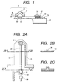
- a probe according to the present invention is a probe for detecting or irradiating evanescent light, and comprises an elastic member (support member) 10 formed on a substrate 21, a tip 5 for evanescence formed on the free end portion of the elastic member, a light-receiving element 19 or laser 20, and a waveguide 28 for optically connecting the light-receiving element 19 or laser 20 and the tip 5.
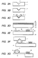
- Figs. 3A to 3G are sectional views showing an example of the manufacturing processes of the probe. The manufacturing method will be explained below with reference to Figs. 3A to 3G.
- a recess portion 3 is formed on the surface of a first substrate 1 consisting of silicon.
- a protection layer 2 is formed on the first substrate 1, and a desired portion of the protection layer 2 is patterned by photolithography and etching to expose the silicon.
- the exposed silicon portion is etched by, e.g., crystallographic axis anisotropic etching, so as to form the recess portion 3.
- silicon dioxide or silicon nitride may be used as the protection layer 2.
- Silicon is preferably etched by crystallographic axis anisotropic etching since it can form a tip 5 with a sharp distal end.
- a potassium hydroxide aqueous solution or the like is used as an etchant, an inverted pyramidal recess portion 3 surrounded by four surfaces equivalent to the (111) face can be formed (see Fig. 3A).
- a peeling layer 4 consisting of an oxide is formed on the first substrate 1 including the recess portion 3 (see Fig. 3B).
- the tip 5 Since the tip 5 is formed on the peeling layer 4 and is then peeled from the peeling layer 4 in a process after formation of the peeling layer 4, a material that allows easy peeling of the material of the tip 5 must be selected for the peeling layer 4. More specifically, the material of the peeling layer 4 must have low reactivity and adhesion with the material of the tip 5.
- Such material includes, for example, BN, AlN, Al 2 O 3 , Si 3 N 4 , SiO 2 , TiN, TiO 2 , VO 2 , Cr 2 O 3 , ZrO 2 , Ta 2 O 5 , WO 3 , and the like. These materials can be formed by sputtering or vacuum evaporation. Especially, when the first substrate 1 consists of silicon, silicon dioxide (SiO 2 ) that can be obtained by oxidizing the substrate surface is preferable.
- the tip 5 is formed on the peeling layer including the recess portion.
- a light transmission material is used for a light transmission portion of the tip 5.
- Such material includes inorganic materials such as SiO 2 , SiN, or the like, and organic materials such as polyimide, and the like.
- a light transmission conductive material such as ITO or the like
- the obtained probe can be used in an SNOM/STM hybrid apparatus that measures resistance by applying a voltage to a sample.
- a peeling assist layer may be formed on the surface of the light transmission layer.
- a metal such as Au or the like may be used.
- a bonding assist layer may be formed on the interface with the bonding layer.
- a metal such as Au or the like may be used.
- the film formation of the individual materials of the tip 5 can use vacuum evaporation, sputtering, chemical vapor deposition, or the like as a thin film formation technique. After film formation, the material of the tip 5 is patterned by known photolithography (Fig. 3C).
- a light-receiving element or laser and its waveguide are formed as a light-emitting or light-receiving mechanism.
- a known silicon process or compound semiconductor process may be used (see Figs. 3D and 3E).
- a bonding layer 26 is formed on the substrate 21 or the elastic member 10 formed on the substrate 21.
- the second substrate 21 and elastic member 10 serve as a member for supporting the tip 5 via the bonding layer 26.
- the bonding layer bonds the tip 5 by pressure, and if the tip 5 and bonding layer 26 consist of metals, a metallic bond can be obtained since they deform against each other by pressure.
- a metal especially, a metal with high ductility and malleability such as Au, Pt, or the like is preferable.
- the material of the tip 5 on the peeling layer 4 including the recess portion 3 is bonded to the bonding layer 26.
- an alignment apparatus which can hold the individual substrates by vacuum chucks and the like, is used. After the tip 5 on the first substrate 1 and the bonding layer 26 on the second substrate 21 are aligned to face each other, they are brought into contact with each other and pressurized, thus bonding the tip 5 and the bonding layer 26 (pressure bonding) (Fig. 3F).
- peeling is done at the interface between the peeling layer 4 and tip 5 to transfer the material of the tip 5 onto the bonding layer 26.
- the tip 5 is peeled from the peeling layer 4 at their interface.
- a micro aperture for detecting or irradiating light is formed at the distal end of the tip 5.
- the tip distal end portion of the light transmission layer covered by a metal layer 7 as a light-shielding layer is brought into contact with a metal substrate, and a voltage is applied across the distal end of the tip 5 and the metal substrate via electrode wiring.
- a coating metal film portion at the distal end of the tip 5 is removed by electric field evaporation or heat fusion, thus forming a micro aperture.
- a tip which used Au as the metal layer 7 and SiO 2 as the light transmission layer, was brought into contact with an Au metal substrate while controlling the elastic deformation amount of an elastic cantilever having an elastic constant of 0.1 [N/m] to 1 [ ⁇ m] or less, i.e., controlling the contact force to 10 -7 [N] or less, and a voltage (crest value: 10 [V], waveform: rectangular wave, time duration: 100 [ ⁇ s], load resistance: 1 [M ⁇ ]) was applied thereto.
- the micro aperture formed had a diameter of about 20 [nm].
- the tip 5 may be formed to have a multilayered structure using materials having different refractive indices, and may be scanned on the sample surface with a load so as to polish the top surface layer, thus forming a micro aperture at the waveguide portion.
- the present invention also includes a surface observation apparatus and recording/reproduction apparatus using the probe manufactured by the above-mentioned processes.
- This probe is brought close to or into contact with a sample and is two-dimensionally scanned by an x-y actuator relative to the sample in the plane of the sample so as to detect evanescent light leaking out through the sample surface. In this way, the surface state of the sample can be observed.
- this probe is used to cause changes in surface state in a micro region on a recording medium, and such changes in surface state are observed, thus realizing a recording/reproduction apparatus.
- the SNOM signal itself can be used in interval control or contact force control with the sample or recording medium.
- a technique such as an optical lever, piezoresistance element, or the like used in an AFM may be used. Also, a technique used in an STM or a technique based on the shear force may be used, and these means do not limit the present invention.
- a surface observation apparatus or recording/reproduction apparatus with a high transfer rate can be provided.
- the magnitude of the contact force between the tip (tip 5) distal end and sample can be controlled to a given value or less while the tip (tip 5) distal end contacts the sample.
- k be the elastic constant of the elastic cantilever
- ⁇ z be the maximum amount of positional variations of the tip distal end in the z-direction.
- the first embodiment is directed to an evanescent light probe and its manufacturing method according to the present invention.
- Figs. 1 and 2A to 2C show the structure of the probe.
- the probe of this embodiment comprises an elastic lever 10 formed on a substrate 21, a tip 5 which is formed on the free end portion of the elastic lever and irradiates evanescent light, a laser 20, and a waveguide 28 for optically connecting the laser 20 and the tip 5.
- Figs. 3A to 3G are sectional views showing the manufacturing processes of the evanescent light probe according to this embodiment.
- a (100) single-crystal silicon wafer was prepared as a first substrate 1.
- a 100-nm thick silicon thermal oxide film was formed as a protection layer 2.
- a desired portion of the protection layer 2 was patterned by photolithography and etching to expose 10- ⁇ m 2 silicon.
- the silicon exposed from the patterned portion was etched by crystallographic axis anisotropic etching using an aqueous potassium hydroxide solution.
- etching conditions were: a 30% aqueous potassium hydroxide solution was used, and a solution temperature of 90°C and an etching time of 10 min were set.
- a inverted pyramidal recess portion 3 having a depth of about 7 ⁇ m and surrounded by four surfaces equivalent to the (111) plane was formed (see Fig. 3A).
- SiO 2 silicon dioxide
- the film formation for the material of the tip 5 was done.
- a 0.1- ⁇ m thick gold (Au) film was formed by vacuum evaporation to obtain a metal film 7, and a 0.6- ⁇ m thick ITO (indium tin oxide) film was formed by sputtering to obtain a light transmission layer 8.
- Au etching used an aqueous solution mixture of Kl and l 2
- ITO etching used an aqueous solution mixture of HCl and FeCl 3 .
- a 0.3- ⁇ m thick gold (Au) film was formed again by vacuum evaporation, and was patterned by photolithography and etching to obtain a bonding assist layer 9 (see Fig. 3C).
- a 300- ⁇ m thick single-crystal n-InP substrate was used as a second substrate 21, and a 1- ⁇ m thick n-InP buffer layer 22, a 0.1- ⁇ m thick InGaAsP active layer 23, a 1.5- ⁇ m thick p-InP cladding layer 24, and a 0.3- ⁇ m thick p-InGaAs capping layer 25 were formed in turn on the substrate 21 by MOCVD (metal organic chemical vapor deposition) (see Fig. 3D).
- MOCVD metal organic chemical vapor deposition
- the obtained multilayered structure was patterned and etched by photolithography to form a ridge structure, thus obtaining a laser 20.
- the wavelength of the laser formed by the above-mentioned method was 1.3 ⁇ m.
- Etching was done by RIBE (reactive ion beam etching) using Cl 2 gas.
- a 3- ⁇ m thick SiO 2 film as a lever material, insulating layer 27, and mask layer 29 was formed on both surfaces of the structure by sputtering.
- the SiO 2 films on both surfaces were patterned and etched by photolithography to form contact holes, a cantilever structure, and a mask layer 29.
- the thickness of the cantilever was 1 ⁇ m.
- a 200-nm thick AuGe film and 300-nm thick Au film were deposited by vacuum evaporation, and were patterned and etched by photolithography to form a bonding layer 26, wiring electrode 33, and output electrode 30 on the substrate side.
- a 3- ⁇ m thick SIO 2 film as a waveguide 28 was deposited by sputtering. The waveguide 28 was then formed by photolithography and etching.
- the etchant used was an aqueous solution mixture of hydrochloric acid (HCl) and phosphoric acid (H 3 PO 4 ). In this case, the projecting portion of the waveguide formed a secondary diffraction grating. From this grating, light inside the waveguide can be output upward.
- the waveguide 28 had a height of 2 ⁇ m and a width of 5 ⁇ m.
- a 50-nm thick Cr film and 300-nm thick Au film were deposited by vacuum evaporation, and were patterned and etched by photolithography to form an output electrode 31 of the capping layer (see Fig. 3E).
- the first and second substrates 1 and 21 were separated from each other to peel the peeling layer 4 and tip 5 at their interface.
- the n-InP substrate was etched from its rear surface using an aqueous HCl solution to form an SiO 2 cantilever. After the formation of the cantilever, the protection film was removed.
- the tip 5 covered by the metal layer 7 was brought into contact with a metal substrate, and a voltage was applied across the tip 5 and metal substrate via the wiring electrode 33 by a voltage application means.
- a micro aperture was formed at the tip distal end portion of the metal layer 7.
- the diameter of the aperture was about 20 nm (see Fig. 3G).
- Fig. 4 shows the arrangement of an observation apparatus using the probe of this embodiment.
- a sample 17 is placed on a holder on an x-y-z scanner.
- the probe of this embodiment is set to oppose the sample 17, and x-y scanning is done while the tip 5 contacts the sample 17.
- evanescent light irradiated from the tip onto the surface of the sample 17 and reflected thereby is focused using an objective lens, and is detected using a photomultiplier, thus allowing surface observation.
- the second embodiment is directed to another evanescent light probe and its manufacturing method according to the present invention.
- Fig. 5 shows the structure of the probe.
- the probe of this embodiment comprises an elastic lever 10 formed on a substrate 21, a tip 5 which is formed on the free end portion of the elastic lever and detects evanescent light, a light-receiving element 19, and a waveguide 28 for optically connecting the light-receiving element 19 and the tip 5.
- the light-receiving element 19 has the same structure as that of the laser 20 used in the first embodiment, and when a reverse electric field is applied, carriers are excited and a current flows in response to incoming light. In this way, evanescent light can be detected.
- a plurality of probes are disposed on the second substrate 21.
- Figs. 6A to 6G are sectional views showing the manufacturing processes of the evanescent light probe according to this embodiment.
- a (100) single-crystal silicon wafer was prepared as a first substrate 1.
- a 100-nm thick silicon thermal oxide film was formed as a protection layer 2.
- a desired portion of the protection layer 2 was patterned by photolithography and etching to expose 10- ⁇ m 2 silicon.
- the silicon exposed from the patterned portion was etched by crystallographic axis anisotropic etching using an aqueous potassium hydroxide solution.
- etching conditions were: a 30% aqueous potassium hydroxide solution was used, and a solution temperature of 90°C and an etching time of 10 min were set. At this time, a inverted pyramidal recess portion 3 having a depth of about 7 ⁇ m and surrounded by four surfaces equivalent to the (111) plane was formed (see Fig. 6A).
- SiO 2 silicon dioxide
- the film formation for the material of the tip 5 was done.
- a 0.1- ⁇ m thick gold (Au) film was formed by vacuum evaporation to obtain a metal film 7, and a 0.6- ⁇ m thick ITO (indium tin oxide) film was formed by sputtering to obtain a light transmission layer 8.
- Au etching used an aqueous solution mixture of Kl and l 2
- ITO etching used an aqueous solution mixture of HCl and FeCl 3 .
- a 0.3- ⁇ m thick gold (Au) film was formed again by vacuum evaporation, and was patterned by photolithography and etching to obtain a bonding assist layer 9 (see Fig. 6C).
- a 300- ⁇ m thick single-crystal n-InP substrate was used as a second substrate 21, and a 1- ⁇ m thick n-InP buffer layer 22, a 0.1- ⁇ m thick InGaAsP active layer 23, a 1.5- ⁇ m thick p-InP cladding layer 24, and a 0.3- ⁇ m thick p-InGaAs capping layer 25 were formed in turn on the substrate 21 by MOCVD (metal organic chemical vapor deposition) (see Fig. 6D).
- MOCVD metal organic chemical vapor deposition
- the obtained multilayered structure was patterned and etched by photolithography to form a ridge structure, thus obtaining a light-receiving element 19.
- Etching was done by RIBE (reactive ion beam etching) using Cl 2 gas.
- a 3- ⁇ m thick SiO 2 film as a lever material, insulating layer 27, and mask layer 29 was formed on both surfaces of the structure by sputtering.
- the SiO 2 films on both surfaces were patterned and etched by photolithography to form contact holes, a cantilever structure, and a mask layer 29.
- the thickness of the cantilever was 1 ⁇ m.
- a 200-nm thick AuGe film and 300-nm thick Au film were deposited by vacuum evaporation, and were patterned and etched by photolithography to form a bonding layer 26, wiring electrode 33, and output electrode 30 on the substrate side.
- Au etching used ion milling to taper the waveguide connection portion of the bonding layer.
- a 3- ⁇ m thick SIO 2 film as a waveguide 28 was deposited by sputtering.
- the waveguide 28 was then formed by photolithography and etching.
- the etchant used was an aqueous solution mixture of hydrochloric acid (HCl) and phosphoric acid (H 3 PO 4 ).
- the waveguide 28 had a height of 2 ⁇ m and a width of 5 ⁇ m.
- a 50-nm thick Cr film and 300-nm thick Au film were deposited by vacuum evaporation, and were patterned and etched by photolithography to form an output electrode 31 of the capping layer (see Fig. 6E).
- the tip 5 on the first substrate 1 and the bonding layer 26 on the second substrate 21 were aligned to face each other, they were brought into contact with each other and were pressurized, thus bonding the tip 5 and the bonding layer 26 (pressure bonding) (Fig. 6F).
- the first and second substrates 1 and 21 were separated from each other to peel the peeling layer 4 and tip 5 at their interface.
- the n-InP substrate was etched from its rear surface using an aqueous HCl solution to form an SiO 2 cantilever. After the formation of the cantilever, the protection film was removed.
- the tip 5 covered by the metal layer 7 was brought into contact with a metal substrate, and a voltage was applied across the tip 5 and metal substrate via the wiring electrode 33 by a voltage application means. Upon application of the voltage, a micro aperture was formed at the tip distal end portion of the metal layer 7. The diameter of the aperture was about 20 nm (see Fig. 6G).
- the micro aperture is formed by forming a metal layer as a light-shielding layer.
- the structure of this embodiment that guides light detected by the tip toward the light-receiving element does not always require the light-shielding layer.
- the light-shielding layer is preferably arranged since the photodetection resolution can be improved.
- Fig. 7 shows the arrangement of an SNOM observation apparatus using the probes of this embodiment.
- a sample 17 is placed on a transparent substrate on an x-y-z scanner.
- the evanescent light components enter the waveguide 28 via the micro apertures of the SNOM probes, and are detected by the light-receiving element 19.
- the detected signals are I/V-converted and are input to a multiplexer to obtain multi SNOM signals.
- the third embodiment is directed to still another evanescent light probe and its manufacturing method according to the present invention.
- Figs. 8, 9A and 9B show the structure of the probe.
- the probe of this embodiment comprises an elastic lever 10 formed on a substrate 21, an evanescent light tip 5 formed on the free end portion of the elastic lever, a light-receiving element 19, a laser 20, and a waveguide 28 for optically connecting the light-receiving element 19 and laser 20 to the tip 5.
- the laser 20 used in the first embodiment and the light-receiving element 19 used in the second embodiment are connected to the tip (tip), return light of evanescent light irradiated from the tip onto a recording medium 18 can be detected.
- a plurality of probes are disposed on the second substrate 21.
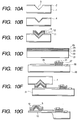
- Figs. 10A to 10G are sectional views showing the manufacturing processes of the evanescent light probe according to this embodiment.
- a (100) single-crystal silicon wafer was prepared as a first substrate 1.
- a 100-nm thick silicon thermal oxide film was formed as a protection layer 2.
- a desired portion of the protection layer 2 was patterned by photolithography and etching to expose 10- ⁇ m 2 silicon.
- the silicon exposed from the patterned portion was etched by crystallographic axis anisotropic etching using an aqueous potassium hydroxide solution. Note that the etching conditions were: a 30% aqueous potassium hydroxide solution was used, and a solution temperature of 90°C and an etching time of 10 min were set. At this time, an inverted pyramidal recess portion 3 having a depth of about 7 ⁇ m and surrounded by four surfaces equivalent to the (111) plane was formed (see Fig. 10A).
- the first substrate 1 was washed using a solution mixture of sulfuric acid and hydrogen peroxide heated to 120°C, and a 2% aqueous hydrofluoric acid solution.
- the first substrate 1 was heated to 1,000°C in an oxygen/hydrogen atmosphere using an oxidization oven to deposit a 500-nm thick silicon dioxide (SiO 2 ) film serving as a peeling layer 4 (see Fig. 10B).
- the film formation for the material of the tip 5 was done. Two different polyimide materials having different refractive indices were prepared. A polyimide film a 11, a polyimide film b 12 serving as a light transmission layer 8, and another polyimide film a 11 were formed all by spin coating. The obtained multilayered structure was patterned by photolithography and etching. In this embodiment, polyimide was used. Alternatively, silicon oxide films having different refractive indices may be formed by sputtering to obtain a layer structure. In this case, different compositions can be obtained by changing the O 2 flow rate upon sputtering, and films having different refractive indices can be formed (see Fig. 10C).
- a 300- ⁇ m thick single-crystal n-InP substrate was used as a second substrate 21, and a 1- ⁇ m thick n-InP buffer layer 22, a 0.1- ⁇ m thick InGaAsP active layer 23, a 1.5- ⁇ m thick p-InP cladding layer 24, and a 0.3- ⁇ m thick p-InGaAs capping layer 25 were formed in turn on the substrate 21 by MOCVD (metal organic chemical vapor deposition) (see Fig. 10D).
- MOCVD metal organic chemical vapor deposition
- the obtained multilayered structure was patterned and etched by photolithography to form a ridge structure, thus obtaining a laser 20. Etching was done by RIBE (reactive ion beam etching) using Cl 2 gas. A 3- ⁇ m thick SiO 2 film as a lever material, insulating layer 27, and mask layer 29 was formed on both surfaces of the structure by sputtering. The SiO 2 films on both surfaces were patterned and etched by photolithography to form contact holes, a cantilever structure, and a mask layer 29. The thickness of the cantilever was 1 ⁇ m.
- a 200-nm thick AuGe film and 300-nm thick Au film were deposited by vacuum evaporation, and were patterned and etched by photolithography to form a bonding layer 26, wiring electrode 33, and output electrode 30 on the substrate side.
- Au etching used ion milling to taper the waveguide connection portion of the bonding layer.
- a 3- ⁇ m thick polyimide film serving as a waveguide 28 was deposited by spin coating.
- the waveguide 28 was then formed by photolithography and etching.
- the waveguide 28 had a height of 2 ⁇ m and a width of 5 ⁇ m.
- a 50-nm thick Cr film and 300-nm Au film were deposited by vacuum evaporation, and were patterned and etched by photolithography to form an output electrode 31 of the capping layer (see Fig. 10E).
- the tip 5 on the first substrate 1 and the bonding layer 26 on the second substrate 21 were aligned to face each other, they were brought into contact with each other and were pressurized, thus bonding the tip 5 and the bonding layer 26 (pressure bonding) (Fig. 10F).
- the first and second substrates 1 and 21 were separated from each other to peel the peeling layer 4 and tip 5 at their interface.
- the n-InP substrate was etched from its rear surface using an aqueous HCl solution to form an SiO 2 cantilever.
- the tip distal end was polished by scanning the sample surface to form a micro aperture having a diameter of about 20 nm on the polyimide layer a 11 to expose the polyimide layer b 12 therefrom.
- a diamond film was formed on the probe surface (Fig. 10G).
- Fig. 11 shows the arrangement of a recording/reproduction apparatus using the probes of this embodiment.
- a recording medium 18 is placed on a holder on an x-y-z scanner.
- the probes of this embodiment are set to oppose the recording medium 18, and x-y scanning is done while the tips 5 contact the recording medium 18.
- An information recording voltage signal is demultiplexed by a demultiplexer, and the demultiplexed signals are supplied to the lasers 20 of the individual probes via V/I conversion circuits, thus making the tips 5 emit evanescent light.
- the laser beam power is increased to change the state of the recording medium.
- the laser beam power is dropped to read information while maintaining the state of the recording medium.
- an azo compound having quinone and hydroquinone groups which forms redox pairs due to cis-trans photoisomerization in response to only incoming light and causes proton movement among these redox pairs upon application of an electric field, as described in Japanese Laid-Open Patent Application No. 2-98849, is known.
- FIG. 12A to 12F show the manufacturing method and structure of the probe.
- the probe of this embodiment comprises an elastic lever 10 formed on a second substrate 21, a tip 5 which is formed on the free end portion of the elastic lever and irradiates evanescent light, a surface-emission laser 20 on the surface of a third substrate bonded to the second substrate 21.
- a tip 5 made up of a metal layer 7, light transmission layer 8, and bonding assist layer 9 was formed (see Figs. 12A, 12B, and 12C).
- a 200- ⁇ m thick single-crystal silicon substrate was prepared as a second substrate 21, and a 300-nm thick silicon dioxide film and 200-nm thick silicon nitride film were deposited on both surfaces of the substrate respectively by thermal oxidation and low-pressure chemical vapor deposition (LPCVD).
- LPCVD thermal oxidation and low-pressure chemical vapor deposition
- the silicon nitride film on the surface was patterned to have a lever shape.
- a 5-nm thick chromium film and 50-nm thick gold film were then deposited and were patterned to form a bonding layer 26 (see Fig. 12D).
- the first and second substrates 1 and 21 were separated from each other to peel the peeling layer 4 and tip 5 at their interface.
- the silicon dioxide film and silicon nitride film on the rear surface were patterned to form an opening.
- the second substrate 21 was etched using an aqueous potassium hydroxide solution, and the silicon dioxide film on the surface was also etched, thus forming a lever 10.
- the tip distal end was polished by scanning the sample surface with a load to form a micro aperture having a diameter of about 20 nm on the metal layer 7, thus exposing the light transmission layer 8 therefrom.
- a third substrate 119 on which light-emitting elements 116 comprising surface-emission lasers were disposed in a matrix at a position corresponding to the tip 5 on the second substrate 21, was prepared.
- the third substrate 119 is obtained by forming anodes 123, cathode 124, active layer 125, mirror layers 126, silicon nitride layer 127, and polyimide layer 128 on a gallium arsenide substrate.
- the anodes 123 are connected to the individual light-emitting elements 116 to independently drive them.
- the silicon nitride layer 127 is formed to attain insulation of the anode 123.
- the cathode 124 is a common electrode.
- the second and third substrates 21 and 119 were bonded to each other using an epoxy resin 118 after they were aligned so that laser beams coming from the light-emitting elements 116 were directly guided to the tip 5 and the opening (see Fig. 12F).
- the multi light probe was manufactured by the above-mentioned processes.
- Fig. 13 shows the arrangement of an exposure apparatus using the multi probe of this embodiment.
- a substrate applied with photoresist is placed on a holder on an x-y-z scanner.
- the probe of this embodiment is set to oppose the photoresist, and x-y scanning is done while the tip 5 contacts the photoresist.
- evanescent light By ON/OFF-controlling evanescent light to be irradiated from the tip 5 onto the photoresist surface, a micropattern can be formed, and high exposure speed can be realized.
- This embodiment has exemplified the probe structure that directly guides light coming from each light-emitting element to the tip.
- a light-receiving element may be formed in place of the light-emitting element, and light detected by the tip may be directly guided to the light-receiving element.
- the light-shielding layer with a micro aperture is not always required, as in the second embodiment.
- the tip is supported by the cantilever.
- the present invention is not limited to such specific support structure.
- a double-supported lever type, torsion lever type, or the like may be used as the support structure.
- the support member In case of the cantilever type and double-supported lever type, the support member must be an elastic member, but in case of the torsion lever type, the support member is not limited to an elastic member.
Landscapes
- Physics & Mathematics (AREA)
- General Physics & Mathematics (AREA)
- Optics & Photonics (AREA)
- Health & Medical Sciences (AREA)
- General Health & Medical Sciences (AREA)
- Nuclear Medicine, Radiotherapy & Molecular Imaging (AREA)
- Radiology & Medical Imaging (AREA)
- Optical Head (AREA)
- Length Measuring Devices By Optical Means (AREA)
Applications Claiming Priority (4)
| Application Number | Priority Date | Filing Date | Title |
|---|---|---|---|
| JP51073/97 | 1997-02-19 | ||
| JP5107397 | 1997-02-19 | ||
| JP10044402A JPH10293134A (ja) | 1997-02-19 | 1998-02-10 | 光検出または照射用のプローブ、及び該プローブを備えた近視野光学顕微鏡・記録再生装置・露光装置、並びに該プローブの製造方法 |
| JP44402/98 | 1998-02-10 |
Publications (1)
| Publication Number | Publication Date |
|---|---|
| EP0860726A1 true EP0860726A1 (de) | 1998-08-26 |
Family
ID=26384304
Family Applications (1)
| Application Number | Title | Priority Date | Filing Date |
|---|---|---|---|
| EP98102899A Withdrawn EP0860726A1 (de) | 1997-02-19 | 1998-02-19 | Spitze Sonde mit Mikroöffnung zur Wahrnehmung oder Abstrahlung von Licht, optisches Nahfeldmikroskop, Aufzeichnungs- und Wiedergabegerät sowie Belichtungsgerät unter Verwendung dieser Sonde und Herstellungsverfahren der Sonde |
Country Status (3)
| Country | Link |
|---|---|
| US (2) | US6201226B1 (de) |
| EP (1) | EP0860726A1 (de) |
| JP (1) | JPH10293134A (de) |
Cited By (14)
| Publication number | Priority date | Publication date | Assignee | Title |
|---|---|---|---|---|
| EP0986057A1 (de) * | 1998-03-24 | 2000-03-15 | Seiko Instruments Inc. | Optischer nahfeldkopf |
| FR2785045A1 (fr) * | 1998-10-23 | 2000-04-28 | Centre Nat Rech Scient | Integration monolithique d'un systeme de detection pour la microscopie en champ proche base sur la reinjection optique dans un laser a cavite verticale emettant par la surface |
| EP1010983A1 (de) * | 1998-06-25 | 2000-06-21 | Japan Science and Technology Corporation | Sonde mit optischen wellenleiter und verfahren zu deren herstellung |
| EP1050740A2 (de) * | 1999-02-17 | 2000-11-08 | CSEM Centre Suisse d'Electronique et de Microtechnique SA | Verfahren zur integrierten Herstellung von an einer Halterung befestigten Spitzen |
| EP1061510A1 (de) * | 1998-11-09 | 2000-12-20 | Seiko Instruments Inc. | Optischer nahfeldkopf und verfahren zu desser herstellung |
| EP1063641A1 (de) * | 1998-02-10 | 2000-12-27 | Seiko Instruments Inc. | Informationsaufzeichnungsgeraet |
| EP1120780A2 (de) * | 2000-01-26 | 2001-08-01 | Seiko Instruments Inc. | Aufzeichnungsmedium, optischer Nahfeldkopf, optische Aufzeichnungsvorrichtung und Verfahren zur Herstellung |
| EP1122722A1 (de) * | 1999-08-25 | 2001-08-08 | Seiko Instruments Inc. | Optischer nahfeldkopf und verfahren zu dessen herstellung |
| US6408122B1 (en) | 1999-10-14 | 2002-06-18 | Canon Kabushiki Kaisha | Probe for irradiating with or detecting light and method for manufacturing the same |
| WO2004068501A2 (de) * | 2003-01-31 | 2004-08-12 | Fraunhofer-Gesellschaft zur Förderung der angewandten Forschung e.V. | Sonde für ein optisches nahfeldmikroskop und verfahren zu deren herstellung |
| WO2004068502A2 (de) * | 2003-01-31 | 2004-08-12 | Fraunhofer-Gesellschaft zur Förderung der angewandten Forschung e.V. | Sonde für ein optisches nahfeldmikroskop mit verbesserter streulichtunterdrückung und verfahren zu deren herstellung |
| EP1780174A1 (de) * | 2005-10-27 | 2007-05-02 | LG Electronics Inc. | Nanodatenschreib- und Lesevorrichtung mit Cantileverstruktur und Herstellungsverfahren dafür |
| EP2026333A1 (de) * | 2007-07-31 | 2009-02-18 | Nitto Denko Corporation | Aufhängungsplatte mit Schaltung |
| US7652972B2 (en) | 2004-07-20 | 2010-01-26 | Lg Electronics Inc. | Nano data writing and reading apparatus using cantilever structure and fabrication method thereof |
Families Citing this family (43)
| Publication number | Priority date | Publication date | Assignee | Title |
|---|---|---|---|---|
| US6339217B1 (en) * | 1995-07-28 | 2002-01-15 | General Nanotechnology Llc | Scanning probe microscope assembly and method for making spectrophotometric, near-field, and scanning probe measurements |
| US5751683A (en) * | 1995-07-24 | 1998-05-12 | General Nanotechnology, L.L.C. | Nanometer scale data storage device and associated positioning system |
| US6337479B1 (en) * | 1994-07-28 | 2002-01-08 | Victor B. Kley | Object inspection and/or modification system and method |
| US6752008B1 (en) | 2001-03-08 | 2004-06-22 | General Nanotechnology Llc | Method and apparatus for scanning in scanning probe microscopy and presenting results |
| US7196328B1 (en) | 2001-03-08 | 2007-03-27 | General Nanotechnology Llc | Nanomachining method and apparatus |
| US6802646B1 (en) * | 2001-04-30 | 2004-10-12 | General Nanotechnology Llc | Low-friction moving interfaces in micromachines and nanomachines |
| JP3949831B2 (ja) * | 1998-11-11 | 2007-07-25 | セイコーインスツル株式会社 | 光カンチレバーとその製造方法 |
| US6852968B1 (en) * | 1999-03-08 | 2005-02-08 | Canon Kabushiki Kaisha | Surface-type optical apparatus |
| JP2001027596A (ja) * | 1999-05-13 | 2001-01-30 | Canon Inc | 走査型プローブによる表面特性・電気的特性の検出装置と検出方法、およびこれらにより構成されたマルチプローブによる表面特性・電気的特性の検出装置と検出方法、並びに観察装置と観察方法 |
| AU6061100A (en) * | 1999-07-01 | 2001-01-22 | General Nanotechnology, Llc | Object inspection and/or modification system and method |
| JP3513448B2 (ja) | 1999-11-11 | 2004-03-31 | キヤノン株式会社 | 光プローブ |
| FR2806527B1 (fr) * | 2000-03-20 | 2002-10-25 | Schlumberger Technologies Inc | Colonne a focalisation simultanee d'un faisceau de particules et d'un faisceau optique |
| JP2002005810A (ja) | 2000-06-16 | 2002-01-09 | Canon Inc | プローブ及びその製造方法、表面観察装置、露光装置、情報処理装置 |
| US6670208B2 (en) * | 2000-06-23 | 2003-12-30 | Nec Corporation | Optical circuit in which fabrication is easy |
| JP2002296169A (ja) | 2001-03-30 | 2002-10-09 | Canon Inc | 近接場光プローブ、及び該近接場光プローブを有する近接場光学顕微鏡、近接場光リソグラフィー装置、近接場光ストレージ装置 |
| JP3902925B2 (ja) * | 2001-07-31 | 2007-04-11 | エスアイアイ・ナノテクノロジー株式会社 | 走査型アトムプローブ |
| JP2003042930A (ja) * | 2001-08-03 | 2003-02-13 | Pioneer Electronic Corp | 近接場光発生素子及びこれを具備してなる光学装置 |
| US7053369B1 (en) * | 2001-10-19 | 2006-05-30 | Rave Llc | Scan data collection for better overall data accuracy |
| US6813937B2 (en) * | 2001-11-28 | 2004-11-09 | General Nanotechnology Llc | Method and apparatus for micromachines, microstructures, nanomachines and nanostructures |
| US7106935B2 (en) * | 2002-01-07 | 2006-09-12 | Seagate Technology Llc | Apparatus for focusing plasmon waves |
| JP3817498B2 (ja) | 2002-06-14 | 2006-09-06 | キヤノン株式会社 | 近接場光用の探針を有するプローブの製造方法 |
| JP3862623B2 (ja) * | 2002-07-05 | 2006-12-27 | キヤノン株式会社 | 光偏向器及びその製造方法 |
| JP2005538855A (ja) * | 2002-09-09 | 2005-12-22 | ジェネラル ナノテクノロジー エルエルシー | 走査型プローブ顕微鏡の流体送達 |
| US6764967B2 (en) * | 2002-10-05 | 2004-07-20 | Taiwan Semiconductor Manufacturing Co., Ltd. | Method for forming low thermal budget sacrificial oxides |
| TWI225923B (en) * | 2003-11-21 | 2005-01-01 | Tatung Co Ltd | Fiber vibration sensor |
| JP2005173411A (ja) * | 2003-12-12 | 2005-06-30 | Canon Inc | 光偏向器 |
| JP4027359B2 (ja) | 2003-12-25 | 2007-12-26 | キヤノン株式会社 | マイクロ揺動体、光偏向器、画像形成装置 |
| US7176450B2 (en) * | 2004-01-02 | 2007-02-13 | Itn Energy Systems, Inc. | Long travel near-field scanning optical microscope |
| KR100566810B1 (ko) * | 2004-04-20 | 2006-04-03 | 한국전자통신연구원 | 근접광 탐침의 제작 방법 |
| WO2005119697A1 (en) * | 2004-05-31 | 2005-12-15 | Givargizov Michail Evgen Evich | Tip structure for scanning devices, method of its preparation and devices thereon |
| KR100584987B1 (ko) * | 2004-10-11 | 2006-05-29 | 삼성전기주식회사 | 표면 플라즈몬파를 이용한 피라미드 형상의 근접장 탐침 |
| US20070041238A1 (en) * | 2005-07-08 | 2007-02-22 | Nanochip, Inc. | High density data storage devices with read/write probes with hollow or reinforced tips |
| JP5232382B2 (ja) * | 2005-12-06 | 2013-07-10 | 株式会社エンプラス | プローブチップ及びプローブカード |
| US7817318B2 (en) * | 2005-12-09 | 2010-10-19 | Canon Kabushiki Kaisha | Oscillating system and optical deflector |
| JP5170983B2 (ja) * | 2006-05-30 | 2013-03-27 | キヤノン株式会社 | 光偏向器、及びそれを用いた光学機器 |
| JP4881073B2 (ja) * | 2006-05-30 | 2012-02-22 | キヤノン株式会社 | 光偏向器、及びそれを用いた光学機器 |
| WO2008105888A2 (en) * | 2006-05-31 | 2008-09-04 | Georgia Tech Research Corporation | Integrated sensing probes, methods of fabrication thereof, and methods of use thereof |
| KR100746961B1 (ko) * | 2006-07-31 | 2007-08-07 | 한국과학기술연구원 | 단백질 키나아제 a 검출용 바이오 센서, 및 이를 포함하는키트 |
| JP2009042737A (ja) * | 2007-07-13 | 2009-02-26 | Canon Inc | 揺動体装置、及びそれを用いた光偏向器 |
| US8277442B2 (en) * | 2008-05-05 | 2012-10-02 | Zila, Inc. | Disposable tip apparatus for laser surgical device |
| US8535300B2 (en) * | 2008-10-24 | 2013-09-17 | Zila, Inc. | Surgical laser tip apparatus with alignment assembly |
| US9268017B2 (en) * | 2011-07-29 | 2016-02-23 | International Business Machines Corporation | Near-field millimeter wave imaging |
| JP2014013160A (ja) * | 2012-07-04 | 2014-01-23 | Hitachi Ltd | 走査プローブ顕微鏡 |
Citations (5)
| Publication number | Priority date | Publication date | Assignee | Title |
|---|---|---|---|---|
| EP0112402A1 (de) * | 1982-12-27 | 1984-07-04 | International Business Machines Corporation | Lichtwellenleiter mit einer Submikronöffnung, Verfahren zur Herstellung des Wellenleiters und Verwendung des Wellenleiters mit einem optischen Speicher |
| US5354985A (en) * | 1993-06-03 | 1994-10-11 | Stanford University | Near field scanning optical and force microscope including cantilever and optical waveguide |
| US5517280A (en) * | 1994-04-12 | 1996-05-14 | The Board Of Trustees Of The Leland Stanford, Jr. University | Photolithography system |
| US5546375A (en) * | 1992-07-15 | 1996-08-13 | Canon Kabushiki Kaisha | Method of manufacturing a tip for scanning tunneling microscope using peeling layer |
| EP0786642A1 (de) * | 1995-09-14 | 1997-07-30 | Canon Kabushiki Kaisha | Herstellungsverfahren einer Mikrospitze zum Wahrnehmen eines Tunnelstromes, einer Mikrokraft oder magnetischen Kraft, Substratform dafür, Herstellungsverfahren einer Sonde mit Mikrospitze, Sondeneinheit, Rastertunnelmikroskop und Informationsaufzeichnungs-/-wiedergabevorrichtung mit einer solchen Sonde |
Family Cites Families (7)
| Publication number | Priority date | Publication date | Assignee | Title |
|---|---|---|---|---|
| JPH0298849A (ja) | 1988-10-04 | 1990-04-11 | Canon Inc | 記録・再生装置及び該装置を用いた記録・再生方法 |
| JP2744339B2 (ja) | 1990-08-03 | 1998-04-28 | キヤノン株式会社 | 情報処理装置及び情報処理方法 |
| JP3000491B2 (ja) * | 1991-04-10 | 2000-01-17 | キヤノン株式会社 | カンチレバーユニット及びこれを用いた情報処理装置、原子間力顕微鏡、磁力顕微鏡 |
| JP3268797B2 (ja) * | 1991-10-09 | 2002-03-25 | オリンパス光学工業株式会社 | 光導入装置 |
| US5348638A (en) * | 1992-01-16 | 1994-09-20 | Matsushita Electric Industrial Co., Ltd. | Method of manufacturing a probe for a scanning tunneling microscope |
| US5770856A (en) * | 1993-07-22 | 1998-06-23 | British Technology Group Ltd | Near field sensor with cantilever and tip containing optical path for an evanescent wave |
| JP3576655B2 (ja) * | 1995-09-14 | 2004-10-13 | キヤノン株式会社 | 微小探針の製造方法及びその製造用雌型基板、並びにその微小探針を有するプローブの製造方法 |
-
1998
- 1998-02-10 JP JP10044402A patent/JPH10293134A/ja active Pending
- 1998-02-18 US US09/025,036 patent/US6201226B1/en not_active Expired - Lifetime
- 1998-02-19 EP EP98102899A patent/EP0860726A1/de not_active Withdrawn
-
2001
- 2001-01-22 US US09/765,374 patent/US6333497B2/en not_active Expired - Lifetime
Patent Citations (5)
| Publication number | Priority date | Publication date | Assignee | Title |
|---|---|---|---|---|
| EP0112402A1 (de) * | 1982-12-27 | 1984-07-04 | International Business Machines Corporation | Lichtwellenleiter mit einer Submikronöffnung, Verfahren zur Herstellung des Wellenleiters und Verwendung des Wellenleiters mit einem optischen Speicher |
| US5546375A (en) * | 1992-07-15 | 1996-08-13 | Canon Kabushiki Kaisha | Method of manufacturing a tip for scanning tunneling microscope using peeling layer |
| US5354985A (en) * | 1993-06-03 | 1994-10-11 | Stanford University | Near field scanning optical and force microscope including cantilever and optical waveguide |
| US5517280A (en) * | 1994-04-12 | 1996-05-14 | The Board Of Trustees Of The Leland Stanford, Jr. University | Photolithography system |
| EP0786642A1 (de) * | 1995-09-14 | 1997-07-30 | Canon Kabushiki Kaisha | Herstellungsverfahren einer Mikrospitze zum Wahrnehmen eines Tunnelstromes, einer Mikrokraft oder magnetischen Kraft, Substratform dafür, Herstellungsverfahren einer Sonde mit Mikrospitze, Sondeneinheit, Rastertunnelmikroskop und Informationsaufzeichnungs-/-wiedergabevorrichtung mit einer solchen Sonde |
Non-Patent Citations (3)
| Title |
|---|
| AKAMINE S ET AL: "LOW TEMPERATURE THERMAL OXIDATION SHARPENING OF MICROCAST TIPS", JOURNAL OF VACUUM SCIENCE AND TECHNOLOGY: PART B, vol. 10, no. 5, 1 September 1992 (1992-09-01), pages 2307 - 2310, XP000322763 * |
| RADMACHER M ET AL: "SCANNING NEARFIELD OPTICAL MICROSCOPE USING MICROFABRICATED PROBES", REVIEW OF SCIENTIFIC INSTRUMENTS, vol. 65, no. 8, 1 August 1994 (1994-08-01), pages 2737/2738, XP000466350 * |
| VAN HULST N F ET AL: "NEAR-FIELD OPTICAL MICROSCOPE USING A SILICON-NITRIDE PROBE", APPLIED PHYSICS LETTERS, vol. 62, no. 5, 1 February 1993 (1993-02-01), pages 461 - 463, XP000335964 * |
Cited By (33)
| Publication number | Priority date | Publication date | Assignee | Title |
|---|---|---|---|---|
| EP1063641A1 (de) * | 1998-02-10 | 2000-12-27 | Seiko Instruments Inc. | Informationsaufzeichnungsgeraet |
| US6950385B1 (en) | 1998-02-10 | 2005-09-27 | Seiko Instruments Inc. | Information recording apparatus |
| EP1063641A4 (de) * | 1998-02-10 | 2005-01-12 | Seiko Instr Inc | Informationsaufzeichnungsgeraet |
| EP0986057A1 (de) * | 1998-03-24 | 2000-03-15 | Seiko Instruments Inc. | Optischer nahfeldkopf |
| EP0986057A4 (de) * | 1998-03-24 | 2000-07-12 | Seiko Instr Inc | Optischer nahfeldkopf |
| US6625109B1 (en) | 1998-03-24 | 2003-09-23 | Seiko Instruments Inc. | Near-field optical head and head support assembly having near-field optical head |
| EP1010983A1 (de) * | 1998-06-25 | 2000-06-21 | Japan Science and Technology Corporation | Sonde mit optischen wellenleiter und verfahren zu deren herstellung |
| EP1010983B1 (de) * | 1998-06-25 | 2008-02-27 | Japan Science and Technology Agency | Sonde mit optischem wellenleiter und herstellungsverfahren dafür |
| WO2000025165A1 (fr) * | 1998-10-23 | 2000-05-04 | Centre National De La Recherche Scientifique - Cnrs | Integration monolithique d'un systeme de detection pour la microscopie en champ proche base sur la reinjection optique dans un laser a cavite verticale emettant par la surface |
| FR2785045A1 (fr) * | 1998-10-23 | 2000-04-28 | Centre Nat Rech Scient | Integration monolithique d'un systeme de detection pour la microscopie en champ proche base sur la reinjection optique dans un laser a cavite verticale emettant par la surface |
| EP1061510A1 (de) * | 1998-11-09 | 2000-12-20 | Seiko Instruments Inc. | Optischer nahfeldkopf und verfahren zu desser herstellung |
| EP1816642A1 (de) | 1998-11-09 | 2007-08-08 | Seiko Instruments Inc. | Nahfeld Abtastkopf und Herstellungsverfahren dafür |
| EP1727138A3 (de) * | 1998-11-09 | 2007-01-10 | Seiko Instruments Inc. | Nahfeld Abtastkopf und Herstellungsverfahren dafür |
| EP1727138A2 (de) * | 1998-11-09 | 2006-11-29 | Seiko Instruments Inc. | Nahfeld Abtastkopf und Herstellungsverfahren dafür |
| US7599277B1 (en) | 1998-11-09 | 2009-10-06 | Seiko Instruments Inc. | Near-field optical head having tapered hole for guiding light beam |
| EP1580738A1 (de) * | 1998-11-09 | 2005-09-28 | Seiko Instruments Inc. | Nahfeld-Abtastkopf und Herstellungsverfahren dafür |
| EP1061510A4 (de) * | 1998-11-09 | 2004-05-19 | Seiko Instr Inc | Nahfeldabtastkopf und herstellungsverfahren |
| EP1050740A3 (de) * | 1999-02-17 | 2001-05-30 | CSEM Centre Suisse d'Electronique et de Microtechnique SA | Verfahren zur integrierten Herstellung von an einer Halterung befestigten Spitzen |
| EP1050740A2 (de) * | 1999-02-17 | 2000-11-08 | CSEM Centre Suisse d'Electronique et de Microtechnique SA | Verfahren zur integrierten Herstellung von an einer Halterung befestigten Spitzen |
| EP1122722A1 (de) * | 1999-08-25 | 2001-08-08 | Seiko Instruments Inc. | Optischer nahfeldkopf und verfahren zu dessen herstellung |
| EP1122722A4 (de) * | 1999-08-25 | 2005-02-09 | Seiko Instr Inc | Optischer nahfeldkopf und verfahren zu dessen herstellung |
| US6408122B1 (en) | 1999-10-14 | 2002-06-18 | Canon Kabushiki Kaisha | Probe for irradiating with or detecting light and method for manufacturing the same |
| EP1120780A2 (de) * | 2000-01-26 | 2001-08-01 | Seiko Instruments Inc. | Aufzeichnungsmedium, optischer Nahfeldkopf, optische Aufzeichnungsvorrichtung und Verfahren zur Herstellung |
| US6697322B2 (en) | 2000-01-26 | 2004-02-24 | Seiko Instruments Inc. | Recording medium, optical recording device utilizing recording medium, and method of manufacturing recording medium |
| EP1120780A3 (de) * | 2000-01-26 | 2003-04-09 | Seiko Instruments Inc. | Aufzeichnungsmedium, optischer Nahfeldkopf, optische Aufzeichnungsvorrichtung und Verfahren zur Herstellung |
| US7477817B2 (en) | 2003-01-31 | 2009-01-13 | Fraunhofer-Gesellschaft Zur Forderung | Probe for an optical near field microscope with improved scattered light suppression and method for producing the same |
| WO2004068502A3 (de) * | 2003-01-31 | 2004-11-04 | Fraunhofer Ges Forschung | Sonde für ein optisches nahfeldmikroskop mit verbesserter streulichtunterdrückung und verfahren zu deren herstellung |
| WO2004068501A2 (de) * | 2003-01-31 | 2004-08-12 | Fraunhofer-Gesellschaft zur Förderung der angewandten Forschung e.V. | Sonde für ein optisches nahfeldmikroskop und verfahren zu deren herstellung |
| WO2004068502A2 (de) * | 2003-01-31 | 2004-08-12 | Fraunhofer-Gesellschaft zur Förderung der angewandten Forschung e.V. | Sonde für ein optisches nahfeldmikroskop mit verbesserter streulichtunterdrückung und verfahren zu deren herstellung |
| WO2004068501A3 (de) * | 2003-01-31 | 2004-11-04 | Fraunhofer Ges Forschung | Sonde für ein optisches nahfeldmikroskop und verfahren zu deren herstellung |
| US7652972B2 (en) | 2004-07-20 | 2010-01-26 | Lg Electronics Inc. | Nano data writing and reading apparatus using cantilever structure and fabrication method thereof |
| EP1780174A1 (de) * | 2005-10-27 | 2007-05-02 | LG Electronics Inc. | Nanodatenschreib- und Lesevorrichtung mit Cantileverstruktur und Herstellungsverfahren dafür |
| EP2026333A1 (de) * | 2007-07-31 | 2009-02-18 | Nitto Denko Corporation | Aufhängungsplatte mit Schaltung |
Also Published As
| Publication number | Publication date |
|---|---|
| US6333497B2 (en) | 2001-12-25 |
| US20010007347A1 (en) | 2001-07-12 |
| JPH10293134A (ja) | 1998-11-04 |
| US6201226B1 (en) | 2001-03-13 |
Similar Documents
| Publication | Publication Date | Title |
|---|---|---|
| US6333497B2 (en) | Probe with tip having micro aperture for detecting or irradiating light, near-field optical microscope, recording/reproduction apparatus, and exposure apparatus using the probe, and method of manufacturing the probe | |
| JP3697034B2 (ja) | 微小開口を有する突起の製造方法、及びそれらによるプローブまたはマルチプローブ | |
| JP3618896B2 (ja) | 微小開口を有するプローブの作製法とそれによるプローブ、並びに該プローブを用いた走査型近接場光顕微鏡と走査型トンネル顕微鏡との複合装置、および該プローブを用いた記録再生装置 | |
| US6982419B2 (en) | Probe with hollow waveguide and method for producing the same | |
| US6211532B1 (en) | Microprobe chip for detecting evanescent waves probe provided with the microprobe chip and evanescent wave detector, nearfield scanning optical microscope, and information regenerator provided with the microprobe chip | |
| JP3554233B2 (ja) | 光プローブの製造方法 | |
| US6408123B1 (en) | Near-field optical probe having surface plasmon polariton waveguide and method of preparing the same as well as microscope, recording/regeneration apparatus and micro-fabrication apparatus using the same | |
| JP3000492B2 (ja) | 情報処理装置 | |
| JP3524343B2 (ja) | 微小開口の形成方法と微小開口を有する突起、及びそれらによるプローブまたはマルチプローブ、並びに該プローブを用いた表面観察装置、露光装置、情報処理装置 | |
| US6408122B1 (en) | Probe for irradiating with or detecting light and method for manufacturing the same | |
| JPH11166935A (ja) | 光検出または照射用の光プローブと該プローブを備えた近視野光学顕微鏡、及該光プローブの製造方法とその製造に用いる基板 | |
| US6337477B1 (en) | Probe having micro-projection and manufacturing method thereof | |
| JP3817498B2 (ja) | 近接場光用の探針を有するプローブの製造方法 | |
| US20080073520A1 (en) | Tip structure for scanning devices, method of its preparation and devices thereon | |
| JPH1186364A (ja) | 微小開口の形成方法、微小開口を含んでなるメンブレンと該メンブレンによるプローブ、及び該プローブによる表面観察装置、露光装置、情報処理装置 | |
| JPH07311207A (ja) | Spmカンチレバー及びその製造方法 | |
| JP2004020349A (ja) | 導波路層構造、導波路層構造を有するプローブの製造方法、該導波路層構造を有するプローブ、該プローブを有するストレージ装置、表面観察装置、露光装置、デバイス製造方法 | |
| JPH11316242A (ja) | 光ファイバプローブおよびその製造方法 | |
| JP2000067462A (ja) | 微小開口を有するプローブ、及び該プローブを有する情報処理装置 |
Legal Events
| Date | Code | Title | Description |
|---|---|---|---|
| PUAI | Public reference made under article 153(3) epc to a published international application that has entered the european phase |
Free format text: ORIGINAL CODE: 0009012 |
|
| AK | Designated contracting states |
Kind code of ref document: A1 Designated state(s): DE FR GB IT |
|
| AX | Request for extension of the european patent |
Free format text: AL;LT;LV;MK;RO;SI |
|
| 17P | Request for examination filed |
Effective date: 19990225 |
|
| AKX | Designation fees paid |
Free format text: DE FR GB IT |
|
| RBV | Designated contracting states (corrected) |
Designated state(s): DE FR GB IT |
|
| 17Q | First examination report despatched |
Effective date: 20030602 |
|
| STAA | Information on the status of an ep patent application or granted ep patent |
Free format text: STATUS: THE APPLICATION IS DEEMED TO BE WITHDRAWN |
|
| 18D | Application deemed to be withdrawn |
Effective date: 20041005 |