EP0856944A2 - System für akustische Oberflächenwelle - Google Patents
System für akustische Oberflächenwelle Download PDFInfo
- Publication number
- EP0856944A2 EP0856944A2 EP98101209A EP98101209A EP0856944A2 EP 0856944 A2 EP0856944 A2 EP 0856944A2 EP 98101209 A EP98101209 A EP 98101209A EP 98101209 A EP98101209 A EP 98101209A EP 0856944 A2 EP0856944 A2 EP 0856944A2
- Authority
- EP
- European Patent Office
- Prior art keywords
- surface acoustic
- acoustic wave
- elements
- substrates
- mounting
- Prior art date
- Legal status (The legal status is an assumption and is not a legal conclusion. Google has not performed a legal analysis and makes no representation as to the accuracy of the status listed.)
- Granted
Links
- 238000010897 surface acoustic wave method Methods 0.000 title claims abstract description 157
- 239000000758 substrate Substances 0.000 claims abstract description 35
- 239000002305 electric material Substances 0.000 claims description 10
- 239000003292 glue Substances 0.000 claims description 7
- 239000011358 absorbing material Substances 0.000 claims description 6
- 239000002390 adhesive tape Substances 0.000 claims description 4
- WSMQKESQZFQMFW-UHFFFAOYSA-N 5-methyl-pyrazole-3-carboxylic acid Chemical compound CC1=CC(C(O)=O)=NN1 WSMQKESQZFQMFW-UHFFFAOYSA-N 0.000 claims description 3
- 239000011248 coating agent Substances 0.000 claims description 3
- 238000000576 coating method Methods 0.000 claims description 3
- 239000013078 crystal Substances 0.000 claims description 3
- PSHMSSXLYVAENJ-UHFFFAOYSA-N dilithium;[oxido(oxoboranyloxy)boranyl]oxy-oxoboranyloxyborinate Chemical compound [Li+].[Li+].O=BOB([O-])OB([O-])OB=O PSHMSSXLYVAENJ-UHFFFAOYSA-N 0.000 claims description 3
- GQYHUHYESMUTHG-UHFFFAOYSA-N lithium niobate Chemical compound [Li+].[O-][Nb](=O)=O GQYHUHYESMUTHG-UHFFFAOYSA-N 0.000 claims description 3
- 238000000034 method Methods 0.000 abstract description 10
- XAGFODPZIPBFFR-UHFFFAOYSA-N aluminium Chemical compound [Al] XAGFODPZIPBFFR-UHFFFAOYSA-N 0.000 description 2
- 229910052782 aluminium Inorganic materials 0.000 description 2
- 238000010586 diagram Methods 0.000 description 2
- 238000004826 seaming Methods 0.000 description 2
- 239000010409 thin film Substances 0.000 description 2
- XUIMIQQOPSSXEZ-UHFFFAOYSA-N Silicon Chemical compound [Si] XUIMIQQOPSSXEZ-UHFFFAOYSA-N 0.000 description 1
- 230000002542 deteriorative effect Effects 0.000 description 1
- 230000000694 effects Effects 0.000 description 1
- 239000000463 material Substances 0.000 description 1
- 230000035939 shock Effects 0.000 description 1
- 229910052710 silicon Inorganic materials 0.000 description 1
- 239000010703 silicon Substances 0.000 description 1
Images


Classifications
-
- H—ELECTRICITY
- H03—ELECTRONIC CIRCUITRY
- H03H—IMPEDANCE NETWORKS, e.g. RESONANT CIRCUITS; RESONATORS
- H03H9/00—Networks comprising electromechanical or electro-acoustic devices; Electromechanical resonators
- H03H9/02—Details
- H03H9/05—Holders; Supports
- H03H9/058—Holders; Supports for surface acoustic wave devices
- H03H9/0585—Holders; Supports for surface acoustic wave devices consisting of an adhesive layer
-
- H—ELECTRICITY
- H01—ELECTRIC ELEMENTS
- H01L—SEMICONDUCTOR DEVICES NOT COVERED BY CLASS H10
- H01L2224/00—Indexing scheme for arrangements for connecting or disconnecting semiconductor or solid-state bodies and methods related thereto as covered by H01L24/00
- H01L2224/01—Means for bonding being attached to, or being formed on, the surface to be connected, e.g. chip-to-package, die-attach, "first-level" interconnects; Manufacturing methods related thereto
- H01L2224/42—Wire connectors; Manufacturing methods related thereto
- H01L2224/47—Structure, shape, material or disposition of the wire connectors after the connecting process
- H01L2224/48—Structure, shape, material or disposition of the wire connectors after the connecting process of an individual wire connector
- H01L2224/4805—Shape
- H01L2224/4809—Loop shape
- H01L2224/48091—Arched
-
- H—ELECTRICITY
- H01—ELECTRIC ELEMENTS
- H01L—SEMICONDUCTOR DEVICES NOT COVERED BY CLASS H10
- H01L2224/00—Indexing scheme for arrangements for connecting or disconnecting semiconductor or solid-state bodies and methods related thereto as covered by H01L24/00
- H01L2224/01—Means for bonding being attached to, or being formed on, the surface to be connected, e.g. chip-to-package, die-attach, "first-level" interconnects; Manufacturing methods related thereto
- H01L2224/42—Wire connectors; Manufacturing methods related thereto
- H01L2224/47—Structure, shape, material or disposition of the wire connectors after the connecting process
- H01L2224/48—Structure, shape, material or disposition of the wire connectors after the connecting process of an individual wire connector
- H01L2224/481—Disposition
- H01L2224/48151—Connecting between a semiconductor or solid-state body and an item not being a semiconductor or solid-state body, e.g. chip-to-substrate, chip-to-passive
- H01L2224/48221—Connecting between a semiconductor or solid-state body and an item not being a semiconductor or solid-state body, e.g. chip-to-substrate, chip-to-passive the body and the item being stacked
- H01L2224/48225—Connecting between a semiconductor or solid-state body and an item not being a semiconductor or solid-state body, e.g. chip-to-substrate, chip-to-passive the body and the item being stacked the item being non-metallic, e.g. insulating substrate with or without metallisation
- H01L2224/48227—Connecting between a semiconductor or solid-state body and an item not being a semiconductor or solid-state body, e.g. chip-to-substrate, chip-to-passive the body and the item being stacked the item being non-metallic, e.g. insulating substrate with or without metallisation connecting the wire to a bond pad of the item
-
- H—ELECTRICITY
- H01—ELECTRIC ELEMENTS
- H01L—SEMICONDUCTOR DEVICES NOT COVERED BY CLASS H10
- H01L2224/00—Indexing scheme for arrangements for connecting or disconnecting semiconductor or solid-state bodies and methods related thereto as covered by H01L24/00
- H01L2224/01—Means for bonding being attached to, or being formed on, the surface to be connected, e.g. chip-to-package, die-attach, "first-level" interconnects; Manufacturing methods related thereto
- H01L2224/42—Wire connectors; Manufacturing methods related thereto
- H01L2224/47—Structure, shape, material or disposition of the wire connectors after the connecting process
- H01L2224/48—Structure, shape, material or disposition of the wire connectors after the connecting process of an individual wire connector
- H01L2224/481—Disposition
- H01L2224/48151—Connecting between a semiconductor or solid-state body and an item not being a semiconductor or solid-state body, e.g. chip-to-substrate, chip-to-passive
- H01L2224/48221—Connecting between a semiconductor or solid-state body and an item not being a semiconductor or solid-state body, e.g. chip-to-substrate, chip-to-passive the body and the item being stacked
- H01L2224/48225—Connecting between a semiconductor or solid-state body and an item not being a semiconductor or solid-state body, e.g. chip-to-substrate, chip-to-passive the body and the item being stacked the item being non-metallic, e.g. insulating substrate with or without metallisation
- H01L2224/48237—Connecting between a semiconductor or solid-state body and an item not being a semiconductor or solid-state body, e.g. chip-to-substrate, chip-to-passive the body and the item being stacked the item being non-metallic, e.g. insulating substrate with or without metallisation connecting the wire to a die pad of the item
-
- H—ELECTRICITY
- H01—ELECTRIC ELEMENTS
- H01L—SEMICONDUCTOR DEVICES NOT COVERED BY CLASS H10
- H01L2924/00—Indexing scheme for arrangements or methods for connecting or disconnecting semiconductor or solid-state bodies as covered by H01L24/00
- H01L2924/15—Details of package parts other than the semiconductor or other solid state devices to be connected
- H01L2924/161—Cap
- H01L2924/1615—Shape
- H01L2924/16152—Cap comprising a cavity for hosting the device, e.g. U-shaped cap
-
- H—ELECTRICITY
- H03—ELECTRONIC CIRCUITRY
- H03H—IMPEDANCE NETWORKS, e.g. RESONANT CIRCUITS; RESONATORS
- H03H9/00—Networks comprising electromechanical or electro-acoustic devices; Electromechanical resonators
- H03H2009/0019—Surface acoustic wave multichip
Definitions
- the present invention relates to a surface acoustic wave system, especially to that having a plurality of surface acoustic wave elements mounted on the same receptacle.
- a typical surface acoustic wave system would have a surface acoustic wave element mounted on a mounting receptacle, the surface acoustic wave element having a surface acoustic wave substrate on which there are formed surface acoustic wave patterns.
- the surface acoustic wave patterns they obtain electric connection through electric wires and the like.
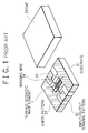
- this particular mounting structure of the surface acoustic wave element for instance, the one disclosed in Japanese Patent Laid-Open Publication No. 3-72708 illustrated in Fig. 1 is common.
- a single surface acoustic wave element 1 is mounted on a substrate 31 where there are provided input/output patterns 32 and an earth pattern 33 obtaining electric connection through bonding wires 34. Being provided the above conditions, the substrate 31 is covered with a cap 35 having hermetic structure. Therefore, when a plurality of surface acoustic wave elements are to be mounted, a number of substrates and caps as many as the surface acoustic wave elements should be provided in mounting the surface acoustic wave elements. Moreover, there has been a proposal for a surface acoustic wave system in which a plurality of surface acoustic wave elements are mounted on a single mounting receptacle.
- the surface acoustic wave elements are individually mounted on the mounting receptacle. Further, regarding the same case in which a plurality of surface acoustic wave elements are to be mounted on the mounting receptacle, there has been proposed a structure in which a plurality of surface acoustic wave element patterns are integrated into one body on a single surface acoustic wave substrate.
- a process of mounting would become easier as a plurality of surface acoustic wave elements are mounted as one body on a single surface acoustic wave substrate.
- a single surface acoustic wave element assembly is to be mounted on a single acoustic wave element substrate which makes the mounting easier than in the case where the surface acoustic wave elements are mounted individually.
- the material of the substrate is naturally limited to one kind of piezo-electric material.
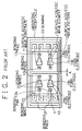
- a structure illustrated in Fig. 2 is taken.
- two surface acoustic wave elements 1 are mounted on a mounting receptacle 2 with a required space A provided in between them.
- a seaming 23 Around the two of the mounted surface acoustic wave elements, there is provided a seaming 23. Bonding pads 21 provided on the mounting receptacle 2 and bonding pads 13a and 13b within surface acoustic wave patterns 12 of the surface acoustic wave elements are electrically connected through bonding wires 22.
- the aforementioned space A is required in between two adjacent surface acoustic wave elements 1 so that the tools used in mounting one surface acoustic wave element would not touch or interfere with the other formerly mounted element. Accordingly, the mounting density within the mounting receptacle 2 is lowered, and so it would be difficult to attempt to miniaturize the scale of the surface acoustic wave system.
- a surface acoustic wave system having a single mounting receptacle on which there are mounted a plurality of surface acoustic wave elements bonded together by the sides of their surface acoustic wave substrates. That is, a plurality of surface acoustic wave elements to be bonded together as one are adhered to one another by the sides of their surface acoustic wave substrates by the use of a glue.
- a plurality of surface acoustic wave elements to be bonded together as one are adhered to one another by the sides of their surface acoustic wave substrates, where there is provided a coating of a sound absorbing material on the upper surface of the bonding region and adhered an adhesive tape on the reverse side of the bonding region.
- Fig. 3 is a plan view showing an internal structure of the surface acoustic wave system according to a first embodiment of the present invention.
- Fig. 4A is plan view and Fig. 4B is a front view of the mounted surface acoustic wave elements.
- each of the two surface acoustic wave elements 1 is constructed by having surface acoustic wave patterns 12 formed on the surface of a surface acoustic wave substrate 11.
- the surface acoustic wave patterns 12 formed on the surface acoustic wave substrates 11 are metallic thin films of aluminum or the like being shaped in certain patterns.
- the surface acoustic wave substrates 11 for the two surface acoustic wave elements are individually made of piezo-electric materials such as lithium niobate, lithium tantalate, crystal, lithium tetraborate and so forth.
- One surface acoustic wave pattern 12 has bonding pads 13a and 13b paired with fork electrodes 14a and 14b respectively.
- the bonding pads 13a and 13b are for obtaining electric connection with the mounting receptacle, and the fork electrodes 14a and 14b are for exciting the surface acoustic waves.
- two surface acoustic wave elements 1 are bonded together as one by the glue 15 to be mounted on the mounting receptacle 2. Therefore, the mounting process is substantially the same as that for mounting one surface acoustic wave element which indicates that the mounting process can be simplified.
- the surface acoustic wave elements are glued together, each of them can have a separate surface acoustic wave substrate of different piezo-electric material. Thus, no restriction is imposed on the system design which provides further flexibility for the system design.
- the space between the two surface acoustic wave elements is as little as that of the thickness generated by the glue, indicating that no useless space is generated in between the surface acoustic wave elements.
- the mounting density can be improved owing to the application of such structure.
- the two surface acoustic wave elements are glued together to become as one body, there is no need for a space in between two surface acoustic wave elements which is originally meant for avoiding interference of tools when mounting is to be done individually.
- an input signal inputted to an external input terminal of the surface acoustic wave system is transmitted to the bonding pad 13a of the surface acoustic wave pattern 12 through the bonding wire 22.
- the signal is to be converted into a surface acoustic wave complying with a certain pattern.
- This surface acoustic wave reaches the fork electrode 14b facing against the fork electrode 14a to be converted into an electric signal that corresponds to a certain pattern form.
- the electric signal is to be transmitted to another bonding pad 21 of the mounting receptacle 2 through the bonding wire 22 to be outputted from an external output terminal of the surface acoustic wave system.
- Fig. 5A is a plan view and Fig. 5B is a front view of the surface acoustic wave element of a second embodiment of the present invention.
- the same reference numerals are given.
- Each of the two surface acoustic wave elements 1 has a separate surface acoustic wave substrate 11 made of a different piezo-electric material where there are formed surface acoustic wave patterns 12 each of which being a metallic thin film such as aluminum formed in a certain pattern.
- the surface acoustic wave pattern 12 comprises bonding pads 13a and 13b for obtaining electric connection with the mounting receptacle, and fork electrodes 14a and 14b for exciting the surface acoustic wave.
- one surface acoustic wave element 1 is to have the side of its surface acoustic wave substrate bonded together with the side of the surface acoustic wave substrate of the neighboring surface acoustic wave element 1.
- On the upper surface of the bonding region where the two surface acoustic wave elements are connected there is provided a coating of a sound absorbing material 16 of a silicon type.
- a wide adhesive tape 17 On the reverse side of this bonding region, there is attached a wide adhesive tape 17. Owing to such structure, the surface acoustic wave elements 1 are bonded together by the sides of their surface acoustic wave substrates 11, to become as one body.
- the surface acoustic wave elements 1 are bonded together to become a single surface acoustic wave element assembly, and this element assembly is mounted on the mounting receptacle in the same manner shown in Fig. 3. Then the bonding pads of the mounting receptacle are to be electrically connected to the bonding pads of the surface acoustic wave patterns through the bonding wires.
- the operation of the surface acoustic wave system of the second embodiment is practically the same as that of the first embodiment.
- the element assembly is mounted on the mounting receptacle. Therefore, the mounting process can be simplified for it is substantially the same as that for mounting a single surface acoustic wave element.
- the surface acoustic wave elements are bonded together, each of them can have a separate surface acoustic wave substrate of different piezo-electric material. Thus, no restriction is imposed on the system design which provides further flexibility for the system design.
- the surface acoustic wave elements bonded together as a single element assembly are closely connected to each other, there is no need for even a glue like in the case of the first embodiment. Therefore, there is practically no space saved in between the surface acoustic wave elements which leads to an advantage that the mounting density can be increased.
- the two surface acoustic wave elements are bonded together as a single element assembly, there is no need for a space in between two surface acoustic wave elements which is originally meant for avoiding interference of tools when mounting is to be done individually.
- shocks generating at the bonding region of the two surface acoustic wave elements are absorbed by the sound absorbing material, and so there is no influence whatsoever given to the surface acoustic wave.
- the sound absorbing material there can be used a glue which will provide the same sort of effect.
- the present invention takes the structure in which a plurality of surface acoustic wave elements are bonded together as a single element assembly by the sides of their surface acoustic wave substrates to be mounted on the mounting receptacle. Consequently, a plurality of surface acoustic wave elements can practically be treated as one surface acoustic wave element concerning the mounting process, resulting in easier mounting and less trouble in mounting the surface acoustic wave elements. Moreover, there is no need for provision of spaces among a plurality of surface acoustic wave elements which makes it possible to increase the mounting density and so miniaturize the surface acoustic wave system.
- the surface acoustic wave elements having surface acoustic wave substrates made of different piezo-electric materials can also be bonded together to form a single element assembly, so as to be treated as a single surface acoustic wave element.
- the system design can become more flexible.
Landscapes
- Physics & Mathematics (AREA)
- Acoustics & Sound (AREA)
- Surface Acoustic Wave Elements And Circuit Networks Thereof (AREA)
- Transducers For Ultrasonic Waves (AREA)
Applications Claiming Priority (3)
| Application Number | Priority Date | Filing Date | Title |
|---|---|---|---|
| JP17988/97 | 1997-01-31 | ||
| JP9017988A JPH10215143A (ja) | 1997-01-31 | 1997-01-31 | 弾性表面波装置 |
| JP1798897 | 1997-01-31 |
Publications (3)
| Publication Number | Publication Date |
|---|---|
| EP0856944A2 true EP0856944A2 (de) | 1998-08-05 |
| EP0856944A3 EP0856944A3 (de) | 2000-08-16 |
| EP0856944B1 EP0856944B1 (de) | 2006-10-25 |
Family
ID=11959113
Family Applications (1)
| Application Number | Title | Priority Date | Filing Date |
|---|---|---|---|
| EP98101209A Expired - Lifetime EP0856944B1 (de) | 1997-01-31 | 1998-01-23 | System für akustische Oberflächenwelle |
Country Status (4)
| Country | Link |
|---|---|
| US (1) | US6075307A (de) |
| EP (1) | EP0856944B1 (de) |
| JP (1) | JPH10215143A (de) |
| DE (1) | DE69836235T2 (de) |
Cited By (1)
| Publication number | Priority date | Publication date | Assignee | Title |
|---|---|---|---|---|
| EP1724920A1 (de) * | 2004-03-12 | 2006-11-22 | Murata Manufacturing Co., Ltd. | Oberflächenwellenbauelement |
Families Citing this family (4)
| Publication number | Priority date | Publication date | Assignee | Title |
|---|---|---|---|---|
| JP4817512B2 (ja) * | 2001-02-28 | 2011-11-16 | 京セラキンセキ株式会社 | 弾性表面波装置 |
| US20040007940A1 (en) * | 2002-07-15 | 2004-01-15 | Asia Pacific Microsystems, Inc. | Thin film acoustic wave device and the manufacturing method thereof |
| JP4712632B2 (ja) * | 2006-07-24 | 2011-06-29 | 太陽誘電株式会社 | 弾性波デバイス及びその製造方法 |
| US8508100B2 (en) * | 2008-11-04 | 2013-08-13 | Samsung Electronics Co., Ltd. | Surface acoustic wave element, surface acoustic wave device and methods for manufacturing the same |
Citations (3)
| Publication number | Priority date | Publication date | Assignee | Title |
|---|---|---|---|---|
| JPH08288786A (ja) * | 1995-04-10 | 1996-11-01 | Nec Corp | 弾性表面波装置 |
| EP0742598A1 (de) * | 1995-05-08 | 1996-11-13 | Matsushita Electric Industrial Co., Ltd. | Verfahren zur Herstellung eines Verbundsubstrats und eine dieses Substrat benutzende piezoelektrischer Anordnung |
| EP0783205A1 (de) * | 1995-07-27 | 1997-07-09 | Daishinku Corporation | Vielfachmoden-piezoelektrisches filter |
Family Cites Families (14)
| Publication number | Priority date | Publication date | Assignee | Title |
|---|---|---|---|---|
| US3701147A (en) * | 1969-01-22 | 1972-10-24 | Us Navy | Surface wave devices for signal processing |
| JPS5242626B2 (de) * | 1973-06-01 | 1977-10-25 | ||
| JPS53145595A (en) * | 1977-05-25 | 1978-12-18 | Nippon Telegr & Teleph Corp <Ntt> | Elastic surface wave oscillator |
| GB2100521B (en) * | 1981-05-13 | 1984-09-12 | Plessey Co Plc | Electrical device package |
| JPS5943826A (ja) * | 1982-09-04 | 1984-03-12 | Sumitomo Metal Ind Ltd | 高靭性電縫鋼管の製造方法 |
| JPS6142943A (ja) * | 1984-08-06 | 1986-03-01 | Clarion Co Ltd | 複合半導体装置の製造方法 |
| JPS6194409A (ja) * | 1984-10-15 | 1986-05-13 | Clarion Co Ltd | 弾性表面波素子の素子分離構造 |
| JPS62105514A (ja) * | 1985-11-01 | 1987-05-16 | Kokusai Denshin Denwa Co Ltd <Kdd> | 弾性表面波フイルタバンク |
| US4931752A (en) * | 1987-09-30 | 1990-06-05 | Hewlett-Packard Company | Polyimide damper for surface acoustic wave device |
| JP2894616B2 (ja) * | 1988-10-31 | 1999-05-24 | 株式会社日立製作所 | 弾性表面波装置及びこれを用いた機器 |
| JPH0314823A (ja) * | 1989-06-13 | 1991-01-23 | Teijin Ltd | 重合体成形物 |
| JPH03293808A (ja) * | 1990-04-11 | 1991-12-25 | Fujitsu Ltd | 弾性表面波素子の製造方法 |
| JPH066175A (ja) * | 1992-06-19 | 1994-01-14 | Murata Mfg Co Ltd | 圧電部品 |
| US5471178A (en) * | 1994-02-03 | 1995-11-28 | Motorola, Inc. | Ladder filter and method for producing conjugately matched impedance |
-
1997
- 1997-01-31 JP JP9017988A patent/JPH10215143A/ja active Pending
-
1998
- 1998-01-23 EP EP98101209A patent/EP0856944B1/de not_active Expired - Lifetime
- 1998-01-23 DE DE69836235T patent/DE69836235T2/de not_active Expired - Lifetime
- 1998-01-29 US US09/015,827 patent/US6075307A/en not_active Expired - Lifetime
Patent Citations (3)
| Publication number | Priority date | Publication date | Assignee | Title |
|---|---|---|---|---|
| JPH08288786A (ja) * | 1995-04-10 | 1996-11-01 | Nec Corp | 弾性表面波装置 |
| EP0742598A1 (de) * | 1995-05-08 | 1996-11-13 | Matsushita Electric Industrial Co., Ltd. | Verfahren zur Herstellung eines Verbundsubstrats und eine dieses Substrat benutzende piezoelektrischer Anordnung |
| EP0783205A1 (de) * | 1995-07-27 | 1997-07-09 | Daishinku Corporation | Vielfachmoden-piezoelektrisches filter |
Non-Patent Citations (1)
| Title |
|---|
| PATENT ABSTRACTS OF JAPAN vol. 018, no. 202 (E-1535), 8 April 1994 (1994-04-08) & JP 06 006175 A (MURATA MFG CO LTD), 14 January 1994 (1994-01-14) * |
Cited By (2)
| Publication number | Priority date | Publication date | Assignee | Title |
|---|---|---|---|---|
| EP1724920A1 (de) * | 2004-03-12 | 2006-11-22 | Murata Manufacturing Co., Ltd. | Oberflächenwellenbauelement |
| EP1724920A4 (de) * | 2004-03-12 | 2009-03-04 | Murata Manufacturing Co | Oberflächenwellenbauelement |
Also Published As
| Publication number | Publication date |
|---|---|
| EP0856944B1 (de) | 2006-10-25 |
| DE69836235D1 (de) | 2006-12-07 |
| US6075307A (en) | 2000-06-13 |
| JPH10215143A (ja) | 1998-08-11 |
| DE69836235T2 (de) | 2007-10-04 |
| EP0856944A3 (de) | 2000-08-16 |
Similar Documents
| Publication | Publication Date | Title |
|---|---|---|
| US4737742A (en) | Unit carrying surface acoustic wave devices | |
| EP0722218B1 (de) | Akustische Oberflächenwellenanordnung | |
| JP3308759B2 (ja) | 弾性表面波装置 | |
| US5949305A (en) | Saw filter encapsulated in a ceramic package with capacitance incorporated therein | |
| JPS6171649A (ja) | Icパツケ−ジ | |
| US4993000A (en) | Surface acoustic wave device | |
| US6075307A (en) | Surface acoustic wave system | |
| US6796181B2 (en) | Acceleration sensor | |
| US4672338A (en) | Saw filter having response enhanced via dampening | |
| JP2000114916A (ja) | 表面弾性波デバイス及びその製造方法 | |
| JP3389530B2 (ja) | 半導体装置 | |
| JPH05251980A (ja) | 弾性表面波デバイスおよびその実装構造 | |
| US6356511B1 (en) | Low distortion ratio hydrophone | |
| JPH026669Y2 (de) | ||
| JP2003037473A (ja) | 弾性表面波装置及びその製造方法 | |
| JP3317926B2 (ja) | 弾性表面波装置 | |
| US6897742B2 (en) | Saw device using different colors or identifiers to distinguish the front and back of the package | |
| JPH0644231U (ja) | 弾性表面波フィルタ | |
| KR100241967B1 (ko) | 탄성표면파소자의 조립방법 | |
| JPH07263996A (ja) | 圧電素子及び圧電部品 | |
| JPS628611A (ja) | 弾性表面波装置 | |
| JPH0716425U (ja) | 弾性表面波フィルタ装置 | |
| JPH05281504A (ja) | 液晶表示パネルの製造方法 | |
| JPH067719B2 (ja) | 超音波トランスジユ−サ | |
| JPH08162898A (ja) | 弾性表面波素子 |
Legal Events
| Date | Code | Title | Description |
|---|---|---|---|
| PUAI | Public reference made under article 153(3) epc to a published international application that has entered the european phase |
Free format text: ORIGINAL CODE: 0009012 |
|
| AK | Designated contracting states |
Kind code of ref document: A2 Designated state(s): DE FR GB IT NL SE |
|
| AX | Request for extension of the european patent |
Free format text: AL;LT;LV;MK;RO;SI |
|
| PUAL | Search report despatched |
Free format text: ORIGINAL CODE: 0009013 |
|
| AK | Designated contracting states |
Kind code of ref document: A3 Designated state(s): AT BE CH DE DK ES FI FR GB GR IE IT LI LU MC NL PT SE |
|
| AX | Request for extension of the european patent |
Free format text: AL;LT;LV;MK;RO;SI |
|
| RIC1 | Information provided on ipc code assigned before grant |
Free format text: 7H 03H 9/05 A, 7H 03H 9/25 B |
|
| 17P | Request for examination filed |
Effective date: 20000705 |
|
| AKX | Designation fees paid |
Free format text: DE FR GB IT NL SE |
|
| 17Q | First examination report despatched |
Effective date: 20041014 |
|
| GRAP | Despatch of communication of intention to grant a patent |
Free format text: ORIGINAL CODE: EPIDOSNIGR1 |
|
| GRAS | Grant fee paid |
Free format text: ORIGINAL CODE: EPIDOSNIGR3 |
|
| GRAA | (expected) grant |
Free format text: ORIGINAL CODE: 0009210 |
|
| AK | Designated contracting states |
Kind code of ref document: B1 Designated state(s): DE FR GB IT NL SE |
|
| REG | Reference to a national code |
Ref country code: GB Ref legal event code: FG4D |
|
| REF | Corresponds to: |
Ref document number: 69836235 Country of ref document: DE Date of ref document: 20061207 Kind code of ref document: P |
|
| PGFP | Annual fee paid to national office [announced via postgrant information from national office to epo] |
Ref country code: SE Payment date: 20070104 Year of fee payment: 10 |
|
| REG | Reference to a national code |
Ref country code: SE Ref legal event code: TRGR |
|
| PGFP | Annual fee paid to national office [announced via postgrant information from national office to epo] |
Ref country code: NL Payment date: 20070131 Year of fee payment: 10 |
|
| ET | Fr: translation filed | ||
| PLBE | No opposition filed within time limit |
Free format text: ORIGINAL CODE: 0009261 |
|
| STAA | Information on the status of an ep patent application or granted ep patent |
Free format text: STATUS: NO OPPOSITION FILED WITHIN TIME LIMIT |
|
| 26N | No opposition filed |
Effective date: 20070726 |
|
| EUG | Se: european patent has lapsed | ||
| NLV4 | Nl: lapsed or anulled due to non-payment of the annual fee |
Effective date: 20080801 |
|
| PG25 | Lapsed in a contracting state [announced via postgrant information from national office to epo] |
Ref country code: NL Free format text: LAPSE BECAUSE OF NON-PAYMENT OF DUE FEES Effective date: 20080801 |
|
| PG25 | Lapsed in a contracting state [announced via postgrant information from national office to epo] |
Ref country code: SE Free format text: LAPSE BECAUSE OF NON-PAYMENT OF DUE FEES Effective date: 20080124 |
|
| REG | Reference to a national code |
Ref country code: GB Ref legal event code: 732E Free format text: REGISTERED BETWEEN 20141023 AND 20141029 |
|
| REG | Reference to a national code |
Ref country code: FR Ref legal event code: TP Owner name: LENOVO INNOVATIONS LIMITED (HONG KONG), HK Effective date: 20141119 |
|
| REG | Reference to a national code |
Ref country code: FR Ref legal event code: PLFP Year of fee payment: 19 |
|
| PGFP | Annual fee paid to national office [announced via postgrant information from national office to epo] |
Ref country code: FR Payment date: 20151208 Year of fee payment: 19 |
|
| PGFP | Annual fee paid to national office [announced via postgrant information from national office to epo] |
Ref country code: IT Payment date: 20160127 Year of fee payment: 19 Ref country code: DE Payment date: 20160119 Year of fee payment: 19 |
|
| PGFP | Annual fee paid to national office [announced via postgrant information from national office to epo] |
Ref country code: GB Payment date: 20160120 Year of fee payment: 19 |
|
| REG | Reference to a national code |
Ref country code: DE Ref legal event code: R119 Ref document number: 69836235 Country of ref document: DE |
|
| GBPC | Gb: european patent ceased through non-payment of renewal fee |
Effective date: 20170123 |
|
| REG | Reference to a national code |
Ref country code: FR Ref legal event code: ST Effective date: 20170929 |
|
| PG25 | Lapsed in a contracting state [announced via postgrant information from national office to epo] |
Ref country code: FR Free format text: LAPSE BECAUSE OF NON-PAYMENT OF DUE FEES Effective date: 20170131 |
|
| PG25 | Lapsed in a contracting state [announced via postgrant information from national office to epo] |
Ref country code: DE Free format text: LAPSE BECAUSE OF NON-PAYMENT OF DUE FEES Effective date: 20170801 Ref country code: GB Free format text: LAPSE BECAUSE OF NON-PAYMENT OF DUE FEES Effective date: 20170123 |
|
| PG25 | Lapsed in a contracting state [announced via postgrant information from national office to epo] |
Ref country code: IT Free format text: LAPSE BECAUSE OF NON-PAYMENT OF DUE FEES Effective date: 20170123 |