EP0853381A2 - Filtre à ondes acoustiques de surface - Google Patents
Filtre à ondes acoustiques de surface Download PDFInfo
- Publication number
- EP0853381A2 EP0853381A2 EP98100309A EP98100309A EP0853381A2 EP 0853381 A2 EP0853381 A2 EP 0853381A2 EP 98100309 A EP98100309 A EP 98100309A EP 98100309 A EP98100309 A EP 98100309A EP 0853381 A2 EP0853381 A2 EP 0853381A2
- Authority
- EP
- European Patent Office
- Prior art keywords
- parallel arm
- electrode
- acoustic wave
- surface acoustic
- wave filter
- Prior art date
- Legal status (The legal status is an assumption and is not a legal conclusion. Google has not performed a legal analysis and makes no representation as to the accuracy of the status listed.)
- Withdrawn
Links
- 238000010897 surface acoustic wave method Methods 0.000 title claims abstract description 102
- 239000000758 substrate Substances 0.000 claims abstract description 26
- 230000000052 comparative effect Effects 0.000 description 17
- 238000003780 insertion Methods 0.000 description 10
- 230000037431 insertion Effects 0.000 description 10
- 238000010276 construction Methods 0.000 description 8
- 238000010586 diagram Methods 0.000 description 7
- 230000007423 decrease Effects 0.000 description 6
- 239000010409 thin film Substances 0.000 description 5
- 239000000919 ceramic Substances 0.000 description 4
- 230000012447 hatching Effects 0.000 description 4
- 238000000034 method Methods 0.000 description 4
- 238000012986 modification Methods 0.000 description 4
- 230000004048 modification Effects 0.000 description 4
- 229910003327 LiNbO3 Inorganic materials 0.000 description 2
- 239000000463 material Substances 0.000 description 2
- 239000007787 solid Substances 0.000 description 2
- 229910012463 LiTaO3 Inorganic materials 0.000 description 1
- 239000000956 alloy Substances 0.000 description 1
- 229910045601 alloy Inorganic materials 0.000 description 1
- 230000005540 biological transmission Effects 0.000 description 1
- 238000004891 communication Methods 0.000 description 1
- 239000013078 crystal Substances 0.000 description 1
- 238000002474 experimental method Methods 0.000 description 1
- 239000010408 film Substances 0.000 description 1
- 239000011810 insulating material Substances 0.000 description 1
- 238000010295 mobile communication Methods 0.000 description 1
- 230000003071 parasitic effect Effects 0.000 description 1
- 239000010453 quartz Substances 0.000 description 1
- VYPSYNLAJGMNEJ-UHFFFAOYSA-N silicon dioxide Inorganic materials O=[Si]=O VYPSYNLAJGMNEJ-UHFFFAOYSA-N 0.000 description 1
Images


Classifications
-
- H—ELECTRICITY
- H03—ELECTRONIC CIRCUITRY
- H03H—IMPEDANCE NETWORKS, e.g. RESONANT CIRCUITS; RESONATORS
- H03H9/00—Networks comprising electromechanical or electro-acoustic devices; Electromechanical resonators
- H03H9/25—Constructional features of resonators using surface acoustic waves
-
- H—ELECTRICITY
- H03—ELECTRONIC CIRCUITRY
- H03H—IMPEDANCE NETWORKS, e.g. RESONANT CIRCUITS; RESONATORS
- H03H9/00—Networks comprising electromechanical or electro-acoustic devices; Electromechanical resonators
- H03H9/02—Details
- H03H9/125—Driving means, e.g. electrodes, coils
- H03H9/145—Driving means, e.g. electrodes, coils for networks using surface acoustic waves
-
- H—ELECTRICITY
- H03—ELECTRONIC CIRCUITRY
- H03H—IMPEDANCE NETWORKS, e.g. RESONANT CIRCUITS; RESONATORS
- H03H9/00—Networks comprising electromechanical or electro-acoustic devices; Electromechanical resonators
- H03H9/46—Filters
- H03H9/64—Filters using surface acoustic waves
-
- H—ELECTRICITY
- H03—ELECTRONIC CIRCUITRY
- H03H—IMPEDANCE NETWORKS, e.g. RESONANT CIRCUITS; RESONATORS
- H03H9/00—Networks comprising electromechanical or electro-acoustic devices; Electromechanical resonators
- H03H9/46—Filters
- H03H9/64—Filters using surface acoustic waves
- H03H9/6423—Means for obtaining a particular transfer characteristic
- H03H9/6433—Coupled resonator filters
- H03H9/6483—Ladder SAW filters
Definitions
- the present invention relates to a surface acoustic wave filter comprising a plurality of SAW (Surface Acoustic Wave) resonators formed on a piezoelectric substrate. More particularly, the present invention relates to a surface acoustic wave filter in which a plurality of SAW resonators form a ladder-type filter circuit.
- SAW Surface Acoustic Wave
- a surface acoustic wave filter comprising a plurality of SAW resonators on a piezoelectric substrate has been known as a high frequency band filter for a mobile communication element.
- Japanese Patent Publication (Kokoku) No. 56-19765 discloses a surface acoustic wave filter in which a plurality of SAW resonators form a ladder type circuit on a piezoelectric substrate.
- the resonance frequency fr of a series arm resonator which forms a ladder-type circuit, is made to coincide with the anti-resonance frequency fa of a parallel arm resonator to which parallel arms are inserted so that the input/output impedance is made to match the characteristic impedance near the coincident frequency, thus forming a pass band.
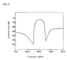
- An example of the attenuation frequency characteristic of this type of surface acoustic wave filter is shown in Fig. 21.
- the electrostatic capacitance of the parallel arm resonator should preferably be increased with respect to the electrostatic capacitance of the series arm resonator (Technical Report of the Institute of Electronics, Information and Communication engineers, US95-25, pp.39-46, July 1995).
- Fig. 22 shows the attenuation frequency characteristic when the ratio of the electrostatic capacitance of the parallel arm resonator to that of the series arm resonator is varied in the surface acoustic wave filter having a ladder-type circuit.
- the characteristics denoted as A to C are obtained by using surface acoustic wave filters A to C having a ladder-type circuit in which the parallel arm resonator has the greater capacitance in order of A to C.
- the present invention is directed to a surface acoustic wave filter that satisfied this need.
- the surface acoustic wave filter comprises a surface acoustic wave filter element and a package.
- the surface acoustic wave filter element include series arm resonators and parallel arm resonators formed on a piezoelectric substrate so as to form a ladder-type circuit which has a series arm having input and output terminals and a plurality of parallel arms between the series arm and a reference potential.
- the package holds the surface acoustic wave filter element therein and has a plurality of electrode lands wired to the surface acoustic wave filter element.
- a plurality of bonding wires by which the input and output terminals and a reference potential terminal of said surface acoustic wave filter element are connected to the plurality of electrode lands of the package, respectively.
- a first one of the parallel arm resonators is connected between the reference potential and a connection point between the input terminal and one of the series arm resonators which is closest to the input terminal, and a second one of the parallel arm resonators is connected between the reference potential and a connection point between the output terminal and one of the series arm resonators which is closest to the output terminal.
- Reference potential electrodes of the first and second parallel arm resonators are connected to first and second of the electrode lands which are formed in the package and which are electrically insulated from each other, respectively, and a reference potential electrode of another one of the parallel arm resonators is short-circuited with the reference potential electrode of the first or second parallel arm resonator within the package.
- a feature of the present invention is that the attenuation amount in the frequency region near the pass band is improved without the insertion loss being increased by devising a method of connecting reference potential electrodes, a method to which attention has hitherto not been paid.
- the reference potential electrode of the parallel arm resonator which is neither the first nor second parallel arm resonator is connected by bonding wire to the first or second electrode land to which the reference potential electrode of the first or second parallel arm resonator is connected.
- the reference potential electrode of the parallel arm resonator which is neither the first nor second parallel arm resonator is electrically short-circuited with the reference potential electrode of the first or second parallel arm resonator on a piezoelectric substrate.
- the reference potential electrode of the parallel arm resonator which is neither the first nor second parallel arm resonator is connected by bonding wire to the first or second electrode land which is short-circuited within the package.
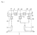
- Fig. 1 shows an equivalent circuit of a surface acoustic wave filter according to a first embodiment of the present invention.
- Fig. 2 is a plan view illustrating the surface acoustic wave filter according to the first embodiment.
- Fig. 3 is a cross-sectional view of the surface acoustic wave filter shown in Fig. 2.
- Fig. 4 is a plan view illustrating external electrodes formed in a package used in the first embodiment.
- Fig. 5 is a circuit diagram of a surface acoustic wave filter of Comparative example 1.
- Fig. 6 is a cross-sectional view of the surface acoustic wave filter of Comparative example 1.
- Fig. 7 is a plan view illustrating conductive patterns within a package in the surface acoustic wave filter of Comparative example 1.
- Fig. 8 is a circuit diagram of a surface acoustic wave filter of Comparative example 2.
- Fig. 9 is a plan view of the surface acoustic wave filter of Comparative example 2.
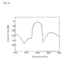
- Fig. 10 shows the attenuation frequency characteristic of the surface acoustic wave filter of Comparative example 1.
- Fig. 11 shows the attenuation frequency characteristic of the surface acoustic wave filter of Comparative example 2.
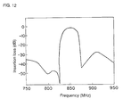
- Fig. 12 shows the attenuation frequency characteristic of the surface acoustic wave filter of the first embodiment.
- Fig. 13 is a plan view illustrating a surface acoustic wave filter according to a second embodiment.
- Fig. 14 is a plan view illustrating a surface acoustic wave filter according to a third embodiment.
- Fig. 15 is a cross-sectional view of the surface acoustic wave filter according to the third embodiment.
- Fig. 16 is a plan view illustrating external electrodes within a package of the surface acoustic wave filter according to the third embodiment.
- Fig. 17 is a circuit diagram illustrating a surface acoustic wave filter according to a fourth embodiment of the present invention.
- Fig. 18 is a plan view illustrating the surface acoustic wave filter according to the fourth embodiment.
- Fig. 19 is a circuit diagram illustrating a modification of the surface acoustic wave filter of the present invention.
- Fig. 20 is a circuit diagram illustrating another modification of the surface acoustic wave filter of the present invention.
- Fig. 21 shows the attenuation frequency characteristic of a conventional surface acoustic wave filter.
- Fig. 22 shows variations of the attenuation frequency characteristic when the capacitance ratio of a parallel arm resonator to a series arm resonator is varied in the conventional surface acoustic wave filter.
- Fig. 1 is a circuit diagram of a first embodiment of a surface acoustic wave filter according to the present invention. As shown in Fig. 1, a series arm 3 is formed between an input terminal and an output terminal 2, and parallel arms 4, 5 and 6 are connected between the series arm 3 and a ground potential.
- Series arm resonators S1 and S2 are inserted in series into the series arm 3.
- the parallel arm 4 is connected between the reference potential and the connection point n1 of the input terminal 1 and the series arm resonator S1, with a parallel arm resonator P1 inserted into the parallel arm 4.
- the parallel arm 5 is connected between the reference potential and the connection point n2 of the series arm resonators S1 and S2, with a parallel arm resonator P2 inserted into the parallel arm 5.
- the parallel arm 6 is connected between the reference potential and the connection point n3 of the series arm resonator S2 and the output terminal 2, with a parallel arm resonator P3 inserted into the parallel arm 6.
- broken line 7 indicates a package, which will be described later.
- the resonators S1 and S2, and P1 to P3 form a ladder-type circuit within the package 7. All of the resonators S1 and S2, and P1 to P3 are a one-port-type SAW resonator.
- the reference potential electrode of the parallel arm resonator P1 is connected to the reference potential via an impedance 11, and the reference potential electrodes of the parallel arm resonators P2 and P3 are short-circuited within the package 7 and further connected to the reference potential via an impedance I2 of the package 7.
- the impedances I1 and I2 indicate impedances due to inductances and parasitic capacitances of bonding wires and package wirings.
- the parallel arm resonator P1 forms a first parallel arm resonator in the present invention
- the parallel arm resonator P3 forms a second parallel arm resonator
- the parallel arm resonator P2 forms a parallel arm resonator other than the first and second parallel arm resonators.
- the reference potential electrode of the first parallel arm resonator P1 and the reference potential electrode of the second parallel arm resonator P3 are individually wired within the package 7, and the reference potential electrode of the parallel arm resonator P2 is electrically short-circuited with the reference potential electrode of the second parallel arm resonator P3 within the package 7.
- the surface acoustic wave filter of this embodiment having the circuit components shown in Fig. 1 is shown in the plan view of Fig. 2 in which a lid member of the package 7 is removed.
- a surface acoustic wave filter 8 is formed using the package 7 of a laminated ceramic package.
- the package 7 may be formed of insulating materials other than a laminated ceramic package.
- the package 7 has an opening 7a, a SAW filter element 9 is fixed within the opening 7a.
- the SAW filter element 9 is formed using a piezoelectric substrate 10.
- the piezoelectric substrate 10 may be formed of a piezoelectric single crystal, such as LiNbO 3 , LiTaO 3 or quartz, or a piezoelectric ceramic, such as a lead zirconate titanate-type piezoelectric ceramic.
- a medium having a piezoelectric thin film such as an insulating substrate having a ZnO thin film thereon on may be used.
- electrodes of the SAW resonator and the like may be formed on either the top surface or the bottom surface of the piezoelectric thin film (i.e., between the piezoelectric thin film and the insulating substrate).
- the series arm resonators S1 and S2 and the parallel arm resonators P1 to P3 are formed at the piezoelectric substrate 10 so as to form a ladder-type circuit shown in Fig. 1.
- All the series arm resonators S1 and S2 and the parallel arm resonators P1 to P3 are formed of a one-port-type SAW resonator such that reflectors are provided on both sides of an interdigital electrode (hereinafter referred to as an "ID electrode") formed of a pair of comb electrodes.
- ID electrode interdigital electrode
- step sections 7b and 7c are formed on both sides of the opening 7a of the package 7.
- the step sections 7b and 7c are raised higher than the bottom of the opening 7a, and electrode lands 11a to 11c, and electrode lands 11d to 11f are formed on the step sections 7b and 7c, respectively.
- the electrode lands 11a to 11c and 11d to 11f are formed of, for example, a conductive film made of Al, Cu or an alloy thereof.
- the electrode land 11b is an electrode land connected to the input terminal 1 shown in Fig. 1, and the electrode land 11e is an electrode land connected to the input terminal 2. More specifically, one comb electrode of the ID electrode of the series arm resonator S1 is connected to the electrode land 11b, and the other comb electrode is connected to one comb electrode of the ID electrode of the series arm resonator S2. The other comb electrode of the series arm resonator S2 is connected to the electrode land 11e by bonding wire 12b.
- the comb electrode on the hot side of the ID electrode of the parallel arm resonator P1 is connected to the series arm resonator S1, and the comb electrode on the grounding side is connected to the electrode land 11a by bonding wire 12c. Further, the comb electrode on the hot side of the ID electrode of the parallel arm resonator P2 is electrically connected to the comb electrode of the series arm resonator S1, and the comb electrode on the grounding side of the parallel arm resonator P2 is connected to the electrode land 11f by bonding wire 12d.
- the comb electrode on the hot side of the second parallel arm resonator P3 is connected to one comb electrode of the ID electrode of the series arm resonator S2, and the comb electrode on the grounding side of the ID electrode of the parallel arm resonator P3 is connected to the electrode land 11f by bonding wire 12e.
- the electrode lands 11a, 11c, 11d and 11f are connected to the ground potential outside the package 7.
- the first parallel arm resonator P1 is connected to the electrode land 11a
- the second parallel arm resonator P3 is connected to the electrode land 11f. That is, the reference potential electrodes of the first and second parallel arm resonators P1 and P3 are connected to different electrode lands 11a and 11f. Further, the reference potential electrode of the parallel arm resonator P2 other than the first and second parallel arm resonators is short-circuited with the reference potential electrode of the second parallel arm resonator P3 via the electrode land 11f.
- the electrode lands 11b and 11e are electrically connected to external electrodes 14b and 14e via through holes 13b and 13e.
- the external electrodes 14b and 14e are provided on the bottom surface of the package 7 and used as electrodes for connection with an external source.
- Fig. 4 shows a plan view of the step portions 7b and 7c of the package 7, where the surface acoustic wave filter element 9 is not inserted.
- the electrode lands 11a to 11f are illustrated with solid hatching lines in Fig. 4 while the external electrodes 14a to 14f positioned below the step sections 7b and 7c are shown with dotted hatching lines.
- the external electrodes 14a, 14c, 14d and 14f are electrically connected to the electrode lands 11a 11c, 11d and 11f on the top surface via the through holes 13a, 13c, 13d and 13f similarly to the external electrodes 14a and 14b shown in Fig. 3.
- the external electrodes 14a, 14c, 14d and 14f are also extended onto the bottom surface through the side surfaces of the package 7.
- the first and second parallel arm resonators P1 and P3 are wired to the first and second electrode lands 11a and 11f which are different electrode lands, and the reference potential electrode of the second parallel arm resonator P3 is electrically wired to the second electrode land 11f. Therefore, it is possible to greatly improve the attenuation amount in the frequency region near the pass band, in particular, in the frequency region lower than the pass band, without causing insertion loss to increase. This will be explained below by contrasting the present invention with Comparative example 1 described in Figs. 5 to 7 and Comparative example 2 described in Figs. 8 and 9.
- a signal input from inside the input terminal leaks to the output terminal 2 side via a line 51 as indicated by an arrow D.
- the resonance point of the parallel arm resonators P1 to P3 namely, in the low frequencies of the pass band
- the impedance of these parallel arm resonators P1 to P3 decreases, the influence of the impedance 13 on the package side becomes large, and the tendency of leakage of the signal becomes noticeable. For this reason, the attenuation in the frequency region lower than the pass band decreases.
- Figs. 6 and 7 correspond to Figs. 3 and 4 which show the package of the surface acoustic wave filter of the first embodiment.
- the external electrodes 14a to 14f connected to the electrode lands 11a to 11f which are connected to the grounding potential via the through holes 13a to 13f are connected in common by a conductive pattern 52.
- Comparative example 2 in which all electrodes to be connected to the ground potential of the first to third parallel arm resonators are separated within the package 7 will be considered.
- the equivalent circuit is as shown in Fig. 8. That is, in the package 7, all electrodes connected to the ground potential of the parallel arm resonators P1 to P3 are separated, and the electrodes are extended to outside the package 7 via impedances 14 to 16 of the package, respectively.
- a line 53 is formed on a circuit substrate to which the surface acoustic wave filter is mounted, and the impedances 16 and 17 indicate impedances on the circuit substrate. Therefore, since the reference potential electrode of the third parallel arm resonator P2 is connected to the ground potential via the impedances 15, 16 and 17, the grounding electrode of the parallel arm resonator P2 is made to float when seen from either of the grounding terminals 54 and 55 on the input and output sides.
- Fig. 9 is a plan view of the surface acoustic wave filter of the comparative example 2 having the circuit components shown in Fig. 8. Components in Fig. 9 which are the same as those of Fig. 2 are given the same reference numerals. As is clear from Fig. 9, electrodes to be connected with the ground potential of the parallel arm resonators P1 to P3 are wired to the different electrode lands 11a, 11d and 11f by bonding wires 12a, 12d', and 12e, respectively.
- electrode lands 11a to 11f are each extended onto the different external electrodes formed on the bottom surface of the package 7 in the same way as in the first embodiment.
- a LiNbO 3 substrate of 64° Y cut X propagation is used, and as the series arm resonators S1 and S2 and the parallel arm resonators P1 to P3, resonators made of Al are formed, and attenuation frequency characteristics are measured.
- a filter is prepared being formed in the same way as in the first embodiment except that the conductive pattern 52 is provided in the package 7.
- comparative example 2 as shown in Fig.
- a filter is prepared being formed in the same way as in the first embodiment except that the grounding potential electrodes of the parallel arm resonators P1 to P3 are connected to the electrode lands 11a, 11d, and 11f by bonding wires. In each case, attenuation frequency characteristics are measured.
- Fig. 10 shows the attenuation frequency characteristics of Comparative example 1.
- Fig. 11 shows the attenuation frequency characteristics of Comparative example 2.
- Fig. 12 shows the attenuation frequency characteristics of the first embodiment.
- Figs. 10 to 12 in the first embodiment (the characteristics of Fig. 12), the attenuation in a region other than the pass band, in particular, the attenuation at the lower frequency than the frequencies of the pass band, is relatively enhanced.
- a comparison between Figs. 10 to 12 shows that the attenuation amount in the low frequencies is enhanced by about 10 dB.
- Fig. 13 illustrates a surface acoustic wave filter according to a second embodiment of the present invention.
- a surface acoustic wave filter 21 a surface acoustic wave filter element 22 having two series arm resonators S1 and S2 and three parallel arm resonators P1 to P3 is used.
- the second embodiment is different from the first embodiment in that the wiring structure of the parallel arm resonators P1 to P3 to the ground potential.
- the components same as explained in the First embodiment are indicated with the same reference numerals used in the first embodiment.
- an electrode to be connected to the ground potential of the series arm resonator P1 is connected to the electrode land 11b by bonding wire 12a.
- An electrode to be connected to the ground potential of the second parallel arm resonator P3 is electrically connected to the electrode land 11f by bonding wire 12e.
- An electrode to be connected to the ground potential of the parallel arm resonator P2 is electrically connected to the electrode which is connected to the ground potential of the second parallel arm resonator P3 by a conductive pattern 23. That is, in Fig.
- the electrode to be connected to the ground potential of the parallel arm resonator P2 is wired to the electrode land 11f by bonding wire 12d
- the electrode to be connected to the ground potential of the parallel arm resonator P2 is short-circuited with the electrode connected to the ground potential of the second parallel arm resonator P3 via the conductive pattern 23. Therefore, the bonding wire 12d shown in Fig. 2 is not used.
- the equivalent circuit is as shown in Fig. 1. Therefore, in the same way as in the first embodiment, the electrodes to be connected to the ground potential of the first and second parallel arm resonators are separated within the package 7, and the electrode connected to the ground potential of the parallel arm resonator P2 is short-circuited with the electrode connected to the ground potential of the second parallel arm resonator P3. This makes it possible to increase the attenuation in the frequency region lower than the pass band.
- FIG. 14 is a plan view illustrating a surface acoustic wave filter according to a third embodiment of the present invention.
- a surface acoustic wave filter 31 includes a surface acoustic wave filter element 32 and a package 7 to hold the surface acoustic wave filter element 32.
- the surface acoustic wave filter element 32 has the series arm resonators S1 and S2 and the parallel arm resonators P1 to P3, which are constructed in the same manner as the surface acoustic wave filter element 9 of the first embodiment.
- the third embodiment is different from the first embodiment in that the electrode of the parallel arm resonator P2 to be connected to the ground potential is wired to the electrode land 11d by bonding wire 12d' and the electrode land 11d and the electrode land 11f are short-circuited with each other within the package 7 by a conductive pattern (which will be described later).
- Fig. 15 is a cross-sectional view of the surface acoustic wave filter 31. Electrode lands 11b and 11e are electrically connected with the external electrodes 14b and 14e via through holes 13b and 13e, respectively. The external electrodes 14b and 14e are extended onto the bottom surface of the package 7.
- Fig. 16 is a plan view illustrating the configuration of electrodes lands 13a to 13f provided on the step sections 7b and 7c and external electrodes 14a to 14f provided under the step sections 7b and 7c.
- the electrode lands 11a to 11f are illustrated with solid hatching lines in Fig. 16 while the external electrodes 14a to 14f are shown with dotted hatching lines.
- the electrode lands 13a to 13f are electrically connected with the external electrodes 14a to 14f via the through holes 13a to 13f, respectively.
- the external electrodes 14a and 14d are electrically connected with electrodes 14c and 14f by conductive patterns 34 and 33, respectively.
- the electrode to be connected to the ground potential of the parallel arm resonator P3 is connected to the electrode land 11d, which is different from the electrode land 11f, via the bonding wire 12d'. Since the electrode land 11d is electrically connected to the electrode land 11f by the conductive pattern 33, the electrode of the parallel arm resonator P3 to be connected to the grounding electrode is short-circuited with the electrode land 11f connected to the electrode of the parallel arm resonator P2 to be connected to the ground potential within the package 7.
- the surface acoustic wave filter 31 of the third embodiment it is also possible to enhance the attenuation in the frequency region lower than the pass band in the same way as in the first embodiment.
- Fig. 17 shows an equivalent circuit of a surface acoustic wave filter according to a fourth embodiment of the present invention.
- Fig. 18 shows a plan view of the surface acoustic wave filter.
- the surface acoustic wave filter according to the fourth embodiment has three series arm resonators S1, S2, and S3 inserted into the series arm 3. Further, four parallel arms 41 to 44 formed between connection points n1, n3, and n5 and a ground potential, respectively, and parallel arm resonators P1 to P4 are inserted into each of the parallel arms 41 to 44. Therefore, the three series arm resonators S1, S2, and S3 and the four parallel arms resonators P1 to P4 are used to form a ladder-type circuit.
- the parallel arm resonator P1 is connected to the connection point n1 between the input terminal 1 and the series arm resonator S1 proximate to the input terminal 1, the parallel arm resonator P1 forms a first parallel arm resonator.
- the parallel arm resonator P4 connected to the connection point n5 of the output terminal 2 and the series arm resonator S3 proximate to the output terminal 2 forms a second parallel arm resonator in the present invention.
- the parallel arm resonators P2 and P3 are parallel arm resonators which are neither the first nor second parallel arm resonator.
- I8 and I9 each indicate an impedance of the package.
- the first parallel arm resonator P1 and the second parallel arm resonator P4 are separated in the package 7 so as to be connected to the ground potential through different paths.
- the parallel arm resonators P2 and P3 which are neither the first nor second parallel arm resonator are connected in common to the second parallel arm resonator P4 via a connection point n6, and connected to the ground potential via the impedance I9.
- Fig. 18 is a plan view illustrating the construction of a surface acoustic wave filter according to a fourth embodiment. Also in a surface acoustic wave filter 45, the package 7 is formed in the same way as the package 7 used in the first embodiment. In a surface acoustic wave filter element 46, three series arm resonators S1 to S3 and four parallel arm resonators P1 to P4 are formed on a piezoelectric substrate 47. For the materials that form the piezoelectric substrate and each resonator, the same materials as those of the first embodiment may be used.
- the parallel arm resonators P1 to P4 are disposed upwards from the bottom. That is, the electrode to be connected to the ground potential in the first parallel arm resonator P1 is wired to the electrode land 11c by bonding wire 48a. The electrode to be connected to the ground potential in the second parallel arm resonator P4 is wired to the electrode land 11d by bonding wire 48b. The electrodes to be connected to the ground potential of the parallel arm resonators P2 and P3 are wired to the electrode land 11f by bonding wires 48c and 48d, respectively.
- One electrode of the series arm resonator S1 is wired to the electrode land 11b which is connected to the input terminal by bonding wire 48e.
- One electrode of the series arm resonator S3 is wired to the electrode land 11e by bonding wire 48f.
- the electrode lands 11d and 11f are short-circuited with each other by a conductive pattern (not shown) within the package 7 in the same manner as in the construction shown in Fig. 16. Therefore, the electrode to be connected to the ground potential in the parallel arm resonators P2 and P3 is connected to the electrode land different from the electrode to be connected to the ground potential in the second parallel arm resonator P4, but the electrode land 11f to which the electrode to be connected to the ground potential in the parallel arm resonators P2 and P3 is connected is short-circuited with the electrode land 11d to which the electrode to be connected to the ground potential in the second parallel arm resonator P4 is connected within the package 7.
- a method in which the electrodes to be connected to the ground potential in the first and second parallel arm resonators are separated and the electrode to be connected to the ground potential in the parallel arm resonator which is neither the first nor second parallel arm resonator is short-circuited with the electrode connected to the ground potential of the first or second parallel arm resonator within the package in the present invention is not limited to the above-described first to fourth embodiments, and can be modified as long as the above-described conditions are met.
- the parallel arm resonator P2 may be connected commonly to the first parallel arm resonator P1 in the package, and the parallel arm resonator P3 may be connected commonly to the second parallel arm resonator P4 in the package so that the connected portions are then wired to the outer side of the package.
- the parallel arm resonators P2 and the second parallel arm resonator P4 may be connected commonly in the package and the parallel arm resonator P3 may be connected commonly to the first parallel arm resonator P1 in the package so that the connected potions are wired to the outer side of the package.
- the electrodes to be connected to the reference potential in the first and second parallel arm resonators are wired to different electrode lands, that is, first and second electrode lands, formed in a package, and the electrode to be connected to the reference potential in the parallel arm resonator which is neither the first nor second parallel arm resonator is short-circuited with the first or second electrode land within the package. Therefore, a decrease in the attenuation amount due to a signal leakage from the input side to the output side is not likely to occur, and a decrease in the attenuation due to the influence of impedance on a substrate on which the surface acoustic wave filter is mounted is not likely to occur.
- the attenuation amount in the frequency region near the pass band can be increased effectively without increasing the insertion loss, it becomes possible to provide a band filter having excellent transmission characteristics.
- an increase in the attenuation outside the pass band can be achieved by merely devising a method of connecting electrodes connected to the reference potential of the parallel arm resonator within a package as described above. Therefore, various modifications are possible, and it is possible to easily realize a connection construction with the reference potential of the first and second parallel arm resonators and the parallel arm resonator which is neither the first nor second parallel arm resonator according to the construction of the surface acoustic wave filter element to be used and the dimensions of the package.
- the parallel arm resonator which is neither the first nor second parallel arm resonator with the electrode to be connected to the reference potential in the first or second parallel arm resonator by connecting the electrode to be connected to the reference potential in the parallel arm resonator which is neither the first nor second parallel arm resonator with the first or second electrode land by bonding wire.
- the electrode to be connected to the reference potential in the parallel arm resonator which is neither the first nor second parallel arm resonator is short-circuited with the electrode to be connected to the reference potential of the first or second parallel arm resonator. Therefore, it is possible to increase the attenuation amount outside the pass band without causing a bonding operation to be complicated after a surface acoustic wave filter element is obtained.
Landscapes
- Physics & Mathematics (AREA)
- Acoustics & Sound (AREA)
- Surface Acoustic Wave Elements And Circuit Networks Thereof (AREA)
Applications Claiming Priority (3)
| Application Number | Priority Date | Filing Date | Title |
|---|---|---|---|
| JP9002527A JPH10200370A (ja) | 1997-01-10 | 1997-01-10 | 弾性表面波フィルタ |
| JP252797 | 1997-01-10 | ||
| JP2527/97 | 1997-01-10 |
Publications (2)
| Publication Number | Publication Date |
|---|---|
| EP0853381A2 true EP0853381A2 (fr) | 1998-07-15 |
| EP0853381A3 EP0853381A3 (fr) | 2000-07-26 |
Family
ID=11531860
Family Applications (1)
| Application Number | Title | Priority Date | Filing Date |
|---|---|---|---|
| EP98100309A Withdrawn EP0853381A3 (fr) | 1997-01-10 | 1998-01-09 | Filtre à ondes acoustiques de surface |
Country Status (4)
| Country | Link |
|---|---|
| US (1) | US6150904A (fr) |
| EP (1) | EP0853381A3 (fr) |
| JP (1) | JPH10200370A (fr) |
| KR (1) | KR100287479B1 (fr) |
Cited By (8)
| Publication number | Priority date | Publication date | Assignee | Title |
|---|---|---|---|---|
| GB2337383A (en) * | 1998-05-14 | 1999-11-17 | Murata Manufacturing Co | Ladder-type filter using SAW resonators |
| EP0961404A3 (fr) * | 1998-05-29 | 2000-08-09 | Fujitsu Limited | Filtre à ondes acoustiques de surface avec suppression améliorée en dehors d'une bande passante |
| EP1050961A3 (fr) * | 1999-03-10 | 2001-06-27 | Murata Manufacturing Co., Ltd. | Dispositif à ondes acoustiques de surface et appareil de communication comportant un tel filtre |
| WO2002017483A1 (fr) | 2000-08-21 | 2002-02-28 | Murata Manufacturing Co.,Ltd. | Dispositif de filtration d'ondes acoustiques de surface |
| WO2005050840A2 (fr) * | 2003-11-20 | 2005-06-02 | Matsushita Electric Industrial Co., Ltd. | Filtre de resonateur piezo-electrique |
| WO2007006375A1 (fr) * | 2005-07-08 | 2007-01-18 | Epcos Ag | Filtre hf a suppression de contre-bande amelioree |
| US7301420B2 (en) | 2003-11-20 | 2007-11-27 | Matsushita Electric Industrial Co., Ltd. | Piezoelectric resonator filter |
| CN1619958B (zh) * | 2003-11-20 | 2011-05-11 | 松下电器产业株式会社 | 使用压电谐振器的滤波器 |
Families Citing this family (24)
| Publication number | Priority date | Publication date | Assignee | Title |
|---|---|---|---|---|
| JP3663898B2 (ja) * | 1997-04-14 | 2005-06-22 | 株式会社村田製作所 | 高周波モジュール |
| FR2785473B1 (fr) * | 1998-10-30 | 2001-01-26 | Thomson Csf | Filtre faibles pertes a ondes acoustiques de surface sur substrat de quartz de coupe optimisee |
| DE19932649A1 (de) * | 1999-07-13 | 2001-02-08 | Epcos Ag | SAW-Filter des Reaktanzfiltertyps mit verbesserter Sperrbereichsunterdrückung und Verfahren zur Optimierung der Sperrbereichsunterdrückung |
| JP2001267881A (ja) * | 2000-03-17 | 2001-09-28 | Fujitsu Media Device Kk | 弾性表面波デバイス及びこれを用いた通信装置、並びにアンテナデュプレクサ |
| JP3363870B2 (ja) * | 2000-05-29 | 2003-01-08 | 沖電気工業株式会社 | 弾性表面波分波器 |
| JP2002151999A (ja) * | 2000-11-09 | 2002-05-24 | Nec Corp | 弾性表面波フィルタ装置および弾性表面波フィルタを収容するためのパッケージ |
| JP3614369B2 (ja) * | 2001-01-11 | 2005-01-26 | 沖電気工業株式会社 | 有極型sawフィルタ |
| EP1296454B1 (fr) * | 2001-09-25 | 2013-05-22 | TDK Corporation | Elément et dispositif à ondes acoustiques de surface |
| JP3980323B2 (ja) * | 2001-10-26 | 2007-09-26 | 沖電気工業株式会社 | 弾性表面波分波器 |
| JP4020644B2 (ja) * | 2002-01-09 | 2007-12-12 | アルプス電気株式会社 | Sawフィルタモジュール |
| JP3913558B2 (ja) * | 2002-01-22 | 2007-05-09 | 沖電気工業株式会社 | 有極型弾性表面波フィルタ |
| US6960966B2 (en) * | 2002-01-22 | 2005-11-01 | Oki Electric Industry Co., Ltd. | Surface acoustic wave filter with attenuation poles |
| JP2003298392A (ja) * | 2002-03-29 | 2003-10-17 | Fujitsu Media Device Kk | フィルタチップ及びフィルタ装置 |
| JP2005094593A (ja) * | 2003-09-19 | 2005-04-07 | Matsushita Electric Ind Co Ltd | 弾性表面波フィルタ |
| KR100750736B1 (ko) | 2004-11-10 | 2007-08-22 | 삼성전자주식회사 | 하나의 트리밍 인덕터를 사용하는 필터 |
| WO2006067935A1 (fr) | 2004-12-24 | 2006-06-29 | Murata Manufacturing Co., Ltd. | Demultiplexeur |
| JP4585431B2 (ja) * | 2005-11-15 | 2010-11-24 | 富士通メディアデバイス株式会社 | 分波器 |
| JP4813984B2 (ja) * | 2006-06-23 | 2011-11-09 | 京セラキンセキ株式会社 | ローパスフィルタ |
| DE102006033709B4 (de) * | 2006-07-20 | 2010-01-14 | Epcos Ag | Elektrisches Modul |
| KR100777451B1 (ko) * | 2006-10-31 | 2007-11-21 | 삼성전자주식회사 | 박막 벌크 음향 공진기 필터 및 듀플렉서 |
| DE102008023374B4 (de) * | 2008-05-13 | 2010-02-11 | Epcos Ag | Filterschaltung mit laddertype-ähnlicher Struktur und Verfahren zu ihrer Optimierung |
| JP6494470B2 (ja) * | 2015-03-18 | 2019-04-03 | 太陽誘電株式会社 | 弾性波デバイス |
| US10218334B2 (en) | 2015-03-18 | 2019-02-26 | Taiyo Yuden Co., Ltd. | Acoustic wave device |
| JP6337867B2 (ja) * | 2015-10-26 | 2018-06-06 | 株式会社村田製作所 | 帯域通過型フィルタ及びデュプレクサ |
Citations (3)
| Publication number | Priority date | Publication date | Assignee | Title |
|---|---|---|---|---|
| EP0541284A1 (fr) * | 1991-10-28 | 1993-05-12 | Fujitsu Limited | Filtre à ondes acoustiques de surface |
| EP0652637A1 (fr) * | 1993-11-05 | 1995-05-10 | Matsushita Electric Industrial Co., Ltd. | Filtre à ondes acoustiques de surface |
| US5914646A (en) * | 1994-03-16 | 1999-06-22 | Fujitsu Limited | Surface acoustic wave filter with larger driving electrode areas in some parallel resonators, and packaging thereof |
Family Cites Families (7)
| Publication number | Priority date | Publication date | Assignee | Title |
|---|---|---|---|---|
| JPS5619765A (en) * | 1979-07-25 | 1981-02-24 | Ricoh Co Ltd | Ink viscosity detecting and controlling device |
| JPH07154201A (ja) * | 1993-11-30 | 1995-06-16 | Matsushita Electric Ind Co Ltd | 弾性表面波フィルタ |
| KR100206037B1 (ko) * | 1994-11-10 | 1999-07-01 | 세끼자와 다다시 | 탄성표면파필터 |
| GB2296614B (en) * | 1994-12-23 | 1999-09-15 | Advanced Saw Prod Sa | Saw filter |
| GB2312109B (en) * | 1996-03-29 | 2000-08-02 | Advanced Saw Prod Sa | Acoustic wave filter |
| JPH10117121A (ja) * | 1996-10-09 | 1998-05-06 | Murata Mfg Co Ltd | Sawフィルタ装置 |
| EP1326333B1 (fr) * | 1997-02-12 | 2008-08-20 | Oki Electric Industry Co., Ltd. | Filtres à ondes acoustiques de surface comportant des pôles d'atténuation, crées par des circuits d'impédance |
-
1997
- 1997-01-10 JP JP9002527A patent/JPH10200370A/ja active Pending
- 1997-12-30 US US09/000,592 patent/US6150904A/en not_active Expired - Lifetime
-
1998
- 1998-01-09 KR KR1019980000376A patent/KR100287479B1/ko not_active IP Right Cessation
- 1998-01-09 EP EP98100309A patent/EP0853381A3/fr not_active Withdrawn
Patent Citations (3)
| Publication number | Priority date | Publication date | Assignee | Title |
|---|---|---|---|---|
| EP0541284A1 (fr) * | 1991-10-28 | 1993-05-12 | Fujitsu Limited | Filtre à ondes acoustiques de surface |
| EP0652637A1 (fr) * | 1993-11-05 | 1995-05-10 | Matsushita Electric Industrial Co., Ltd. | Filtre à ondes acoustiques de surface |
| US5914646A (en) * | 1994-03-16 | 1999-06-22 | Fujitsu Limited | Surface acoustic wave filter with larger driving electrode areas in some parallel resonators, and packaging thereof |
Non-Patent Citations (1)
| Title |
|---|
| MINEYOSHI S ET AL: "ANALYSIS AND OPTIMAL SAW LADDER FILTER DESIGN INCLUDING BONDING WIRE AND PACKAGE IMPEDANCE" IEEE ULTRASONICS SYMPOSIUM PROCEEDINGS,US,NEW YORK, NY: IEEE,1997, pages 175-178, XP000848470 ISBN: 0-7803-4154-6 * |
Cited By (17)
| Publication number | Priority date | Publication date | Assignee | Title |
|---|---|---|---|---|
| GB2337383B (en) * | 1998-05-14 | 2000-03-29 | Murata Manufacturing Co | Surface acoustic wave filter, duplexer, and communication device |
| US6150900A (en) * | 1998-05-14 | 2000-11-21 | Murata Manufacturing Co, Ltd | Surface acoustic wave filter duplexer and communications apparatus utilizing edge reflection of SH-type waves |
| GB2337383A (en) * | 1998-05-14 | 1999-11-17 | Murata Manufacturing Co | Ladder-type filter using SAW resonators |
| US6388545B1 (en) | 1998-05-29 | 2002-05-14 | Fujitsu Limited | Surface-acoustic-wave filter having an improved suppression outside a pass-band |
| EP0961404A3 (fr) * | 1998-05-29 | 2000-08-09 | Fujitsu Limited | Filtre à ondes acoustiques de surface avec suppression améliorée en dehors d'une bande passante |
| EP1050961A3 (fr) * | 1999-03-10 | 2001-06-27 | Murata Manufacturing Co., Ltd. | Dispositif à ondes acoustiques de surface et appareil de communication comportant un tel filtre |
| US6369672B1 (en) | 1999-03-10 | 2002-04-09 | Murata Manufacturing Co., Ltd. | Surface acoustic wave filter and communications apparatus using the same |
| EP1313218A1 (fr) * | 2000-08-21 | 2003-05-21 | Murata Manufacturing Co., Ltd. | Dispositif de filtration d'ondes acoustiques de surface |
| WO2002017483A1 (fr) | 2000-08-21 | 2002-02-28 | Murata Manufacturing Co.,Ltd. | Dispositif de filtration d'ondes acoustiques de surface |
| EP1313218A4 (fr) * | 2000-08-21 | 2009-08-05 | Murata Manufacturing Co | Dispositif de filtration d'ondes acoustiques de surface |
| WO2005050840A2 (fr) * | 2003-11-20 | 2005-06-02 | Matsushita Electric Industrial Co., Ltd. | Filtre de resonateur piezo-electrique |
| WO2005050840A3 (fr) * | 2003-11-20 | 2005-11-10 | Matsushita Electric Ind Co Ltd | Filtre de resonateur piezo-electrique |
| US7301420B2 (en) | 2003-11-20 | 2007-11-27 | Matsushita Electric Industrial Co., Ltd. | Piezoelectric resonator filter |
| CN1619958B (zh) * | 2003-11-20 | 2011-05-11 | 松下电器产业株式会社 | 使用压电谐振器的滤波器 |
| WO2007006375A1 (fr) * | 2005-07-08 | 2007-01-18 | Epcos Ag | Filtre hf a suppression de contre-bande amelioree |
| US8179211B2 (en) | 2005-07-08 | 2012-05-15 | Epcos Ag | RF-filter with improved adjacent channel suppression |
| DE102005032058B4 (de) * | 2005-07-08 | 2016-12-29 | Epcos Ag | HF-Filter mit verbesserter Gegenbandunterdrückung |
Also Published As
| Publication number | Publication date |
|---|---|
| JPH10200370A (ja) | 1998-07-31 |
| US6150904A (en) | 2000-11-21 |
| KR100287479B1 (ko) | 2001-04-16 |
| KR19980070429A (ko) | 1998-10-26 |
| EP0853381A3 (fr) | 2000-07-26 |
Similar Documents
| Publication | Publication Date | Title |
|---|---|---|
| US6150904A (en) | Surface acoustic wave filter having reference potential package electrode lands which are electrically isolated | |
| US7283016B2 (en) | Balanced acoustic wave filter and acoustic wave filter | |
| US7479846B2 (en) | Duplexer | |
| US7116187B2 (en) | Saw element and saw device | |
| US6919777B2 (en) | Surface acoustic wave filter device | |
| US5999069A (en) | Surface acoustic wave ladder filter having a parallel resonator with a larger electrostatic capacitance | |
| US6057744A (en) | Surface acoustic wave device with mutiple pass bands | |
| JP2002300003A (ja) | 弾性波フィルタ | |
| JPH09167937A (ja) | 弾性表面波フィルタ | |
| US7944329B2 (en) | Acoustic wave filter device with branched ground wiring sandwiching the IDT area | |
| US7868716B2 (en) | Acoustic wave filter apparatus | |
| JP2000261344A (ja) | 弾性表面波フィルタ、それを用いた通信機装置 | |
| JPH0697727B2 (ja) | 弾性表面波フィルタ | |
| JPH09321573A (ja) | 弾性表面波フィルタ装置 | |
| KR100511221B1 (ko) | 탄성 표면파 장치 및 통신 장치 | |
| JPWO2004112246A1 (ja) | 弾性表面波分波器 | |
| JP3869919B2 (ja) | 弾性表面波装置 | |
| US6943649B2 (en) | Surface acoustic wave filter with a ground pattern partially surrounding a signal pad and communication device using same | |
| JP3981590B2 (ja) | 弾性表面波フィルタ素子、弾性表面波フィルタ素子用ベース基板及び弾性表面波フィルタ素子を備える弾性表面波装置 | |
| JP3948550B2 (ja) | 弾性表面波装置 | |
| JPH0832402A (ja) | 弾性表面波装置、移動無線機用分波器および移動無線装置 | |
| JP4359978B2 (ja) | ラダー型弾性表面波フィルタ | |
| JP3895397B2 (ja) | Sawフィルタの基板実装方法 | |
| JPH10327039A (ja) | 弾性表面波装置 | |
| JPH10200363A (ja) | 弾性表面波装置及びその製造方法 |
Legal Events
| Date | Code | Title | Description |
|---|---|---|---|
| PUAI | Public reference made under article 153(3) epc to a published international application that has entered the european phase |
Free format text: ORIGINAL CODE: 0009012 |
|
| 17P | Request for examination filed |
Effective date: 19980109 |
|
| AK | Designated contracting states |
Kind code of ref document: A2 Designated state(s): DE FI FR GB SE |
|
| AX | Request for extension of the european patent |
Free format text: AL;LT;LV;MK;RO;SI |
|
| PUAL | Search report despatched |
Free format text: ORIGINAL CODE: 0009013 |
|
| AK | Designated contracting states |
Kind code of ref document: A3 Designated state(s): AT BE CH DE DK ES FI FR GB GR IE IT LI LU MC NL PT SE |
|
| AX | Request for extension of the european patent |
Free format text: AL;LT;LV;MK;RO;SI |
|
| AKX | Designation fees paid |
Free format text: DE FI FR GB SE |
|
| RAP1 | Party data changed (applicant data changed or rights of an application transferred) |
Owner name: MURATA MANUFACTURING CO., LTD. |
|
| 17Q | First examination report despatched |
Effective date: 20071107 |
|
| STAA | Information on the status of an ep patent application or granted ep patent |
Free format text: STATUS: THE APPLICATION IS DEEMED TO BE WITHDRAWN |
|
| 18D | Application deemed to be withdrawn |
Effective date: 20100320 |