EP0851411A2 - Dünnschicht-Magnetkopf und magnetisches Aufnahme/Wiedergabe-Gerät - Google Patents
Dünnschicht-Magnetkopf und magnetisches Aufnahme/Wiedergabe-Gerät Download PDFInfo
- Publication number
- EP0851411A2 EP0851411A2 EP97122699A EP97122699A EP0851411A2 EP 0851411 A2 EP0851411 A2 EP 0851411A2 EP 97122699 A EP97122699 A EP 97122699A EP 97122699 A EP97122699 A EP 97122699A EP 0851411 A2 EP0851411 A2 EP 0851411A2
- Authority
- EP
- European Patent Office
- Prior art keywords
- magnetic
- film
- membrane
- head
- recording
- Prior art date
- Legal status (The legal status is an assumption and is not a legal conclusion. Google has not performed a legal analysis and makes no representation as to the accuracy of the status listed.)
- Granted
Links
Images


Classifications
-
- G—PHYSICS
- G11—INFORMATION STORAGE
- G11B—INFORMATION STORAGE BASED ON RELATIVE MOVEMENT BETWEEN RECORD CARRIER AND TRANSDUCER
- G11B5/00—Recording by magnetisation or demagnetisation of a record carrier; Reproducing by magnetic means; Record carriers therefor
- G11B5/127—Structure or manufacture of heads, e.g. inductive
- G11B5/31—Structure or manufacture of heads, e.g. inductive using thin films
- G11B5/3109—Details
- G11B5/313—Disposition of layers
- G11B5/3143—Disposition of layers including additional layers for improving the electromagnetic transducing properties of the basic structure, e.g. for flux coupling, guiding or shielding
-
- G—PHYSICS
- G11—INFORMATION STORAGE
- G11B—INFORMATION STORAGE BASED ON RELATIVE MOVEMENT BETWEEN RECORD CARRIER AND TRANSDUCER
- G11B5/00—Recording by magnetisation or demagnetisation of a record carrier; Reproducing by magnetic means; Record carriers therefor
- G11B5/127—Structure or manufacture of heads, e.g. inductive
- G11B5/33—Structure or manufacture of flux-sensitive heads, i.e. for reproduction only; Combination of such heads with means for recording or erasing only
- G11B5/39—Structure or manufacture of flux-sensitive heads, i.e. for reproduction only; Combination of such heads with means for recording or erasing only using magneto-resistive devices or effects
- G11B5/3903—Structure or manufacture of flux-sensitive heads, i.e. for reproduction only; Combination of such heads with means for recording or erasing only using magneto-resistive devices or effects using magnetic thin film layers or their effects, the films being part of integrated structures
- G11B5/3967—Composite structural arrangements of transducers, e.g. inductive write and magnetoresistive read
-
- B—PERFORMING OPERATIONS; TRANSPORTING
- B82—NANOTECHNOLOGY
- B82Y—SPECIFIC USES OR APPLICATIONS OF NANOSTRUCTURES; MEASUREMENT OR ANALYSIS OF NANOSTRUCTURES; MANUFACTURE OR TREATMENT OF NANOSTRUCTURES
- B82Y10/00—Nanotechnology for information processing, storage or transmission, e.g. quantum computing or single electron logic
-
- B—PERFORMING OPERATIONS; TRANSPORTING
- B82—NANOTECHNOLOGY
- B82Y—SPECIFIC USES OR APPLICATIONS OF NANOSTRUCTURES; MEASUREMENT OR ANALYSIS OF NANOSTRUCTURES; MANUFACTURE OR TREATMENT OF NANOSTRUCTURES
- B82Y25/00—Nanomagnetism, e.g. magnetoimpedance, anisotropic magnetoresistance, giant magnetoresistance or tunneling magnetoresistance
-
- G—PHYSICS
- G11—INFORMATION STORAGE
- G11B—INFORMATION STORAGE BASED ON RELATIVE MOVEMENT BETWEEN RECORD CARRIER AND TRANSDUCER
- G11B19/00—Driving, starting, stopping record carriers not specifically of filamentary or web form, or of supports therefor; Control thereof; Control of operating function ; Driving both disc and head
- G11B19/20—Driving; Starting; Stopping; Control thereof
- G11B19/2009—Turntables, hubs and motors for disk drives; Mounting of motors in the drive
-
- G—PHYSICS
- G11—INFORMATION STORAGE
- G11B—INFORMATION STORAGE BASED ON RELATIVE MOVEMENT BETWEEN RECORD CARRIER AND TRANSDUCER
- G11B5/00—Recording by magnetisation or demagnetisation of a record carrier; Reproducing by magnetic means; Record carriers therefor
- G11B5/127—Structure or manufacture of heads, e.g. inductive
- G11B5/31—Structure or manufacture of heads, e.g. inductive using thin films
- G11B5/3109—Details
- G11B5/312—Details for reducing flux leakage between the electrical coil layers and the magnetic cores or poles or between the magnetic cores or poles
-
- G—PHYSICS
- G11—INFORMATION STORAGE
- G11B—INFORMATION STORAGE BASED ON RELATIVE MOVEMENT BETWEEN RECORD CARRIER AND TRANSDUCER
- G11B5/00—Recording by magnetisation or demagnetisation of a record carrier; Reproducing by magnetic means; Record carriers therefor
- G11B5/62—Record carriers characterised by the selection of the material
- G11B5/68—Record carriers characterised by the selection of the material comprising one or more layers of magnetisable material homogeneously mixed with a bonding agent
- G11B5/70—Record carriers characterised by the selection of the material comprising one or more layers of magnetisable material homogeneously mixed with a bonding agent on a base layer
- G11B5/706—Record carriers characterised by the selection of the material comprising one or more layers of magnetisable material homogeneously mixed with a bonding agent on a base layer characterised by the composition of the magnetic material
- G11B5/70605—Record carriers characterised by the selection of the material comprising one or more layers of magnetisable material homogeneously mixed with a bonding agent on a base layer characterised by the composition of the magnetic material metals or alloys
- G11B5/70621—Record carriers characterised by the selection of the material comprising one or more layers of magnetisable material homogeneously mixed with a bonding agent on a base layer characterised by the composition of the magnetic material metals or alloys containing Co metal or alloys
-
- G—PHYSICS
- G11—INFORMATION STORAGE
- G11B—INFORMATION STORAGE BASED ON RELATIVE MOVEMENT BETWEEN RECORD CARRIER AND TRANSDUCER
- G11B5/00—Recording by magnetisation or demagnetisation of a record carrier; Reproducing by magnetic means; Record carriers therefor
- G11B5/62—Record carriers characterised by the selection of the material
- G11B5/68—Record carriers characterised by the selection of the material comprising one or more layers of magnetisable material homogeneously mixed with a bonding agent
- G11B5/70—Record carriers characterised by the selection of the material comprising one or more layers of magnetisable material homogeneously mixed with a bonding agent on a base layer
- G11B5/712—Record carriers characterised by the selection of the material comprising one or more layers of magnetisable material homogeneously mixed with a bonding agent on a base layer characterised by the surface treatment or coating of magnetic particles
-
- G—PHYSICS
- G11—INFORMATION STORAGE
- G11B—INFORMATION STORAGE BASED ON RELATIVE MOVEMENT BETWEEN RECORD CARRIER AND TRANSDUCER
- G11B5/00—Recording by magnetisation or demagnetisation of a record carrier; Reproducing by magnetic means; Record carriers therefor
- G11B5/127—Structure or manufacture of heads, e.g. inductive
- G11B5/33—Structure or manufacture of flux-sensitive heads, i.e. for reproduction only; Combination of such heads with means for recording or erasing only
- G11B5/39—Structure or manufacture of flux-sensitive heads, i.e. for reproduction only; Combination of such heads with means for recording or erasing only using magneto-resistive devices or effects
- G11B2005/3996—Structure or manufacture of flux-sensitive heads, i.e. for reproduction only; Combination of such heads with means for recording or erasing only using magneto-resistive devices or effects large or giant magnetoresistive effects [GMR], e.g. as generated in spin-valve [SV] devices
-
- G—PHYSICS
- G11—INFORMATION STORAGE
- G11B—INFORMATION STORAGE BASED ON RELATIVE MOVEMENT BETWEEN RECORD CARRIER AND TRANSDUCER
- G11B5/00—Recording by magnetisation or demagnetisation of a record carrier; Reproducing by magnetic means; Record carriers therefor
- G11B5/127—Structure or manufacture of heads, e.g. inductive
- G11B5/31—Structure or manufacture of heads, e.g. inductive using thin films
- G11B5/3109—Details
- G11B5/3116—Shaping of layers, poles or gaps for improving the form of the electrical signal transduced, e.g. for shielding, contour effect, equalizing, side flux fringing, cross talk reduction between heads or between heads and information tracks
-
- G—PHYSICS
- G11—INFORMATION STORAGE
- G11B—INFORMATION STORAGE BASED ON RELATIVE MOVEMENT BETWEEN RECORD CARRIER AND TRANSDUCER
- G11B5/00—Recording by magnetisation or demagnetisation of a record carrier; Reproducing by magnetic means; Record carriers therefor
- G11B5/127—Structure or manufacture of heads, e.g. inductive
- G11B5/31—Structure or manufacture of heads, e.g. inductive using thin films
- G11B5/3109—Details
- G11B5/312—Details for reducing flux leakage between the electrical coil layers and the magnetic cores or poles or between the magnetic cores or poles
- G11B5/3123—Details for reducing flux leakage between the electrical coil layers and the magnetic cores or poles or between the magnetic cores or poles by using special coil configurations or conductors
Definitions
- Present invention relates to a magnetic recording apparatus using a computer and an information processor, especially relates to a suitable new thin film magnetic head and recording reproducing separate type magnetic head and magnetic storage playback equipment.
- a semiconductor storage means and a magnetic storage means are mainly used. From the viewpoint of access time the semiconductor storage means is used for an internal storage apparatus, and from a viewpoint of large capacity and non-volatility the magnetic storage means is used for an external recording apparatus.
- dominant magnetic memories are a magnetic disk and a magnetic tape.
- a magnetic thin film is formed on an aluminum substrate or on a resin tape.
- a function unit having an electromagnetic converting function is used. Further, a function unit utilizing a magneto-resistance phenomenon or a giant magneto-resistance phenomenon or electromagnetic induction phenomenon is used in order to regenerate the magnetic information.
- the magnetic head is composed of a writing-in portionfor writing in magnetic information and a regenerating portion.
- the writing-in portion is composed of a coil and magnetic poles magnetically coupled and enveloping the coil from upside and downside.
- a magnetic shield layer Between the writing-in portion and the regenerating portion, there is provided a magnetic shield layer. Further, these function units are formed on a magnetic head main body through a base layer.
- the electromagnetic conversion function is utilized in the recording and the magnetoresistance effect is utilized in the reproducing, and a reproducing of the magnetism information is performed by detecting the electromagnetic induction current induced in a coil established in a write department. In this case recording and a reproducing may be performed in one function part.
- Performance of a storage apparatus is determined by speed at input and output operation and storage capacity, and in order to improve competitiveness of the product it is inevitable to shorten the access time and to increase the capacity.
- reduction of size of the storage apparatus becomes important from requirement to reduce weight and size of an information apparatus in recent years.
- the problem of the side fringe magnetic field may be prevented to some extent by notching the lowermagnetic film and forming a pedestal pole tip. It is shown in Japanese Patent Laid-open No. 7-262519 that the pedestal is provided on the pole tip in order to reduce the side fringe. Moreover, high saturation magnetic moment material is provided on the pedestal pole tip layer, and second schield layer is explained as the material of low saturation moment of Permalloy. That is, the lower magnetic film is constructed with two layers of high saturation / low saturation magnetic moment. However, it is not mentioned about resistivity of the magnetic film at all. Accordingly when radio frequency recording is considered, the above invention may not be satisfied with, and the resistivity and the saturation flux density become an important matter.
- the storage density of 2Gb/ in 2 may be provided.
- a problem occurres as follows, and it became clear that the higher density is not attained.
- This problem includes a problem to affect manufacture technology to narrow magnetic pole width and a magnetical problem occurred by making the magnetic pole width narrow.
- the magnetic pole constituting a magnetic gap is needed to generate (leak) magnetic field which is necessary in order to let magnetization of the recording media turn over.
- This magnetic field is decided by a magnetic parameter called magnetic coercive force of the recording media, and it is neccessary to be strengthened in a media for high density recording of late years. Accordingly, volume of the magnetic pole part should not be reduced in order to provide strong magnetic field. That is, thickness of magnetic pole should not be constructed to be thin even if the magnetic pole width is narrowed.
- the material which is generally used as magnetic pole materials is Ni-Fe alloying. As for this material, dry etching of reactivity is difficult. On this account, the magnetic pole of thick film may not be formed. So it is fitted in formation of the magnetic pole, and galvanizing method is used. In the galvanizing method, it will be masked with regist pattern with beforeh, and Ni-Fe is grown up selectively only on the magnetic pole part that the electric pole for a galvanizing exposes out. Accordingly, in order to form minute magnetic pole pattern less than 2 ⁇ m, a regist pattern needs to be formed by a width less than 2 ⁇ m beforehand.
- thickness of the mask pattern needs to be higher than a galvanizing height in order to maintain function as the masking in the galvanizing.
- the galvanizing masking pattern receiving constraint of height , width is formed with an approach exposure method.
- resolution limit of this method is about 2 ⁇ m (when thickness is about 5 ⁇ m), the pattern with less than this resolution limit may not be formed (expensive manufacture method of X-rays lithography methods is not consider here). On this account there is the problem that cannot produce magnetic head for high density recording in a thing of conventional method.
- a magnetic path resistance of the gap neighborhood increases when the magnetic pole width is narrowed. Therefore, as the magnetic pole width is narrowed, magnetic flux flows in the lower magnetic film from the upper magnetic film, the magnetic field which it is necessary does not occur from thea gap department, and a problem occurs. Moreover, if writing frequency is raised in order to realize the high density recording, a problem arises as that writing efficiency falls. That is, an eddy current is easy to occur to the magnetic pole department, magnetic path resistance increases by this affect, and the writing efficiency falls.
- the magnetic gap applys only to the metal membrane, and in the next, the magnetic path may not be formed with a high resistance membrane or Amorphous membrane which induces a little eddy current. It is a common weak point of the conventional magnetic head which makes the magnetic pole with a galvanizing method that the magnetic path cannot be formed with high resistance membrane or amorphous membrane generating a little eddy current.
- an object of the present invention is to provide a thin film magnetic head, a recording reproducing separate type magnetic head, and a magnetic storage head formed a magnetic film of high resistivity partially to pole end of a magnetic storage head.
- a thin film magnetic head applied athe present invention having an upper magnetic film and a lower magnetic film arranged through a non-magnetic gap membrane
- at least an end part of said upper magnetic film or said lower magnetic film is constructed with two or more layers of magnetic films, resistivity of one of said two or more layers is higher than that of other of said two or more layers
- at least an end part of said upper magnetic film or said lower magnetic film is constructed with two or more layers of magnetic membrane
- resistivity of one of said two or more layers of magnetic membrane arranged apart from said non-magnetic gap membrane is higher than resistivity of other of said two or more layers of magnetic membrane connected to said non-magnetic gap membrane, and end parts of said upper magnetic film and said lower magnetic film shape convex, and at least one part of said upper magnetic film or said lower magnetic film has a resistivity more than 50 ⁇ cm.
- a recording reproducing separate type magnetic head having a recording head for writing in information, a reproducing head for reading out the information, and a magnetic shield provided therebetween, said recording head has an upper magnetic film and a lower magnetic film arranged through a non-magnetic magnetic gap membrane, at least an end part of said upper magnetic film or said lower magnetic film is constructed with two or more layers of magnetic membrane, resistivity of one of said two or more layers is higher than that of other of said two or more layers, resistivity of one of said two or more layers of magnetic membrane arranged apart from said non-magnetic gap membrane, is higher than resistivity of other of said two or more layers of magnetic membrane connected to said non-magnetic gap membrane, at least one part of said upper magnetic film or said lower magnetic film has a resistivity more than 50 ⁇ cm, and said reproducing head has a ferromagnetic body and an antiferromagnetic body having a uni-directional anisotropism connected to said ferromagnetic body, at least one part of said antiferrom
- a thin film magnetic disk turns with a speed more than 4000 rpm in recording / reproducing and recording frequency is 45 MHz or more
- said magnetic storage apparatus having said thin film magnetic disk for recording information, a rotation means for rotating said thin film magnetic disk, a recording reproducing separate type magnetic head having a recording head provided on a floating type slider and writing in information and a reproducing head for reading out the information, and a transfer means for supporting and transfering said floating type slider for said film magnetic disk
- said recording head has an upper magnetic film and a lower magnetic film arranged through a non-magnetic magnetic gap membrane, at least an end part of said upper magnetic film or said lower magnetic film is constructed with two or more layers of magnetic membrane,resistivity of one of said two or more layers is higher than that of other of said two or more layers,resistivity of one of said two or more layers of magnetic membrane arranged apart from said non-magnetic gap membrane, is higher than resistivity of other of said two or more layers of magnetic membrane connected to said
- the lower magnetic film serves as a schield membrane with a reproducing head such as MR or GMR
- a gap membrane of non-magnetism is formed between the upper magnetic film and the lower magnetic film
- one part of the lowermagnetic film or the upper magnetic film is made with a dry process such as a suputtering method or vacuum evaporation coating, preferably resistivity more than 80 ⁇ cm is provided
- a flame of galvanizing membrane is formed of SiO 2 , the width thereof decides a track width for recording, and the track width is less than 1.5 ⁇ m.
- a magnetic film having high resistivity more than 80 ⁇ cm is more than saturation flux density 1.5 T
- the magnetic film end over/under the gap membrane is processed by RIE, and the width of a magnetic film over/under the gap membrane is arranged.
- the magnitude of magnetostriction constant of a magnetic film having high resistivity more than 80 ⁇ cm is 1 ⁇ 10 -7 or less furthermore, and the film thickness more than a part of 0.5 ⁇ m of top and bottom magnetic film is formed with high resistivity membrane. It is desirable that a part of the magnetic film of high resistivity is broader than one part of the magnetic film of the low resistivity relating to the width of the magnetic films viewed from a looming side.
- the saturation flux density of the magnetic film is 1.5 T or more.
- a magnetic head having a good recording characteristic may be offered using the material which can be mass-produced. It is difficult to form, with a galvanizing method, a thick (about 3 ⁇ m) membrane having high resistivity and high saturation flux density to be satisfied with these characteristic, and a membrane which consists of 3d transition metal having a small magnetostriction constant (1 ⁇ 10 -7 or less).
- a magnetic film to be satisfied with these characteristic adds oxygen and nitrogen in Fe series, FeCo series or FeNiCo series, and it becomes possible to control the magnetostriction constant using other alloy element.
- an eddy current may be made small by forming with multi-layer or mixed layer film with the ferromagnetism alloying membrane of Fe series, FeCo series or FeNiCo series and with the oxide such as Al2O3 and SiO 2 .
- the magnetic field strength that is one of the performance of the recording head becomes higher by making a part nearest to the gap in the core into high Bs than making a remote part from the gap into high Bs.
- the magnetism characteristic of magnetic film nearby the floating side of the gap influences to the performance effectively, it is effective as the recording head of a narrow track width (less than1.5 ⁇ m) to have a configuration that a part which came in contact with the gap membrane from the floating side (the gap neighborhood) is provided with high Bs, and a part except the high Bs membrane is provided with high ⁇ (even low Bs is good).
- the width of the magnetic film to contact with the gap membrane needs to be formed in a width corresponding to value of the track width.
- the distance of the galvanizing flame decides the width of the galvanizing membrane namely the track width, it becomes possible to form the galvanizing membrane of 0.3-1.5 ⁇ m width.
- Fe, Ni, Co and these binary or ternary alloying membrane are capable to be formed easily, and the membrane (CoNiFe alloying, NiFe alloying) of high Bs (1.5 T or greater) is formed too, the galvanizing membrane may be applied to one part of the magnetic core which comes in contact with the gap membrane which decided track width or may be disposed near the gap membrane.
- the resistivity ⁇ of this galvanizing membrane is 50 ⁇ cm or so, and the resistivity ⁇ in the case of the membrane more than Bs 1.3T by adding ternary transition metal chemical element is about 60 ⁇ cm and the resistivity ⁇ in the case of the galvanizing membrane more than Bs 0.9T by adding metalloid chemical element becomes about 100 ⁇ cm.
- High Bs membrane is necessary for a magnetic film of 1 and 5 in Fig. 3 as mentioned above, and if the resistivity ⁇ of the magnetic films 12 and 5 is high value, the resistivity ⁇ of the magnetic film1 and 5 does not need to be high.
- a membrane is formed by the suputtering method in one part of a lower part magnetic film 11, of high resistivity (80 ⁇ cm or greater), high Bs >1.5 T, and magnetostriction constant (magnitude) ⁇ 1 ⁇ 10 -7 , and a non-magnetic film of 0.1 to 0.2 ⁇ m is formed by a suputtering method thereon as a gap membrane 4.
- a foundation 3 of the galvanizing membrane is formed by the suputtering method in the addition. This foundation 3 may be formed with a high resistivity membrane.
- a regist flame 2 is formed on the foundation 3, and the upper part magnetic film is made with the galvanizing method.
- the track width is fixed with distance between the flames, and it is identified to be capable to form it without composition fluctuation to 0.5 ⁇ m by a flame galvanizing method
- side fringe may be reduced by removing one part of the foundation 3, the gap membrane 4 and the lower part magnetic film (upper part screening membrane of MR and GMR) without re-adhesion.
- Film thickness of high resistivity membrane may restrain degradation of the magnetic field strength, that is to say, the recording performance in a radio frequency by forming it 0.5 to 3 times or more of the film thickness of the gap membrane.
- the membranes over and under the gap 4 (lower part magnetic film 5 and upper part magnetic film 1) are formed with the galvanizing method, recording performance may be raised by making high resistivity membrane with a membrane being wider and thicker than that of the lower part magnetic film 5 or the upper part magnetic film 1.
- a high resistivity membrane 12 is formed on one part of the flame and on the upper part magnetic film 1 by the suputtering method.
- the gap membrane is provided with an electroconductive non-magnetic film (Cr alloying etc.).
- Fig. 4 shows a similar configuration as that in Fig. 1, and thin high resistivity, high Bs membrane 12 is formed on gap 4 by the galvanizing method. Film thickness is a half to three times of the gap, and if the film is constructed within the thickness of this range, the effect of the high resistivity is distinctly arisen in the recording performance and the galvanizing becomes possible, too.
- This high resistivity galvanizing membrane 12 is a ferromagnetism alloying membrane including chemical elements such as P, B, O etc.
- the magnetic film 13 and the magnetic film 14 up and under the gap membrane are made with a galvanizing method.
- Bs of the above magnetic film 13 and 14 is higher than Bs of high resistivity membrane (one part 11 of the shielding membrane and one part of the upper part magnetic film) made by the suputtering methods.
- the magnetic field strength from the gap becomes high by making Bs of the magnetic film near to the gap membrane high, and the radio frequency characteristic is improved by high ⁇ magnetic film (11,12) made by the suputtering method.
- Fig. 5 the magnetic film 13 and the magnetic film 14 up and under the gap membrane are made with a galvanizing method.
- Bs of the above magnetic film 13 and 14 is higher than Bs of high resistivity membrane (one part 11 of the shielding membrane and one part of the upper part magnetic film) made by the suputtering methods.
- the magnetic field strength from the gap becomes high by making Bs of the magnetic film near to the gap membrane high, and the radio frequency characteristic is improved by high ⁇ magnetic film (11,
- the width of the magnetic film 13 and gap membrane 14 and magnetic film 14 (when it was watched from floating side) is narrower than the width of the magnetic film (11 and 12) apart from the gap membrane 14 further, thereby magnetic field gradient of the recording head capable to be made large.
- Recording head in present invention is constituted to be sandwiched the magnetic film of the gap department mutually with the convex magnetic poles disposed face to face as stated above.
- the upper part magnetic pole has a convex configuration and becomes convex against the lower part magnetic pole
- the lower part magnetic pole has a convex configuration and becomes convex against the upper part magnetic pole
- the convex portions of the upper part magnetic pole and the lower part magnetic pole are arranged to be face to face
- width center of the convex part of the upper part magnetic pole and width center of the convex part of the lower part magnetic pole are respectively arranged to be on a same line, and it is desirable to make the height of the convex part low compared with the width of the convex part. It is desirable to produce the recording head of the present invention by following production process.
- the reproducing head in the present invention is constructed with said magnetoresistance effect type element, Soft magnetism membrane and hard magnetism membrane mutually decline 90 degree in magnetic field directions thereof, and the magnetic field of the magnetic film forming a free layer may changes 0-180 degrees from the magnetic field of the magnetic film forming a fixed layer by magnetic field from recording media.
- a magnetic recording apparatus is used, the magnetic head of said magnetic recording apparatus is loaded the magnetoresistance effect element using huge magnetoresistance effect as a means corresponding to high recording density.
- the antiferromagnetism membrane which produces replacement coupling bias should be developped by directly laminating the magnetism membrane.
- main component of the antiferromagnetism membrane is composed with chrome and manganese.
- composition of the ferromagnetic body is provided with cobalt or cobalt alloying comprising cobalt as a main component.
- Co-Fe-Ni alloying is good for the composition of the cobalt alloying when it is used as soft magnetic material,moreover, Co-Pt alloying is good when it is used as high coercive force material.
- it in order to harmonize a direction of one direction anisotropism, it is heat-treated.
- the fifth especially it is effective for spin valve type magnetoresistance effect membrane.
- the hard magnetism layer to contact with the antiferromagnetism layer is constructed with a laminating body of the hard magnetism layer of three layers or more, or total thickness is composed to be not less than 3nm so that heat deterioration of the characteristic of the magnetoresistance effect may be prevented.
- the magnetic recording reproducing device uses the magnetoresistance effect element stated above in the reproducing part, high recording density namely, that is, recording wave length recorded on high recording medium becomes short, and width of recording track becomes narrow with sufficient reproducing capacity and recording may be kept well.
- magnetoresistance effect element in the present invention is realized a fixed bias or a longitudinal bias with the antiferromagnetic substance of chrome group alloying, or the antiferromagnetic substance of Mn group alloying and the cobalt series ferromagnetic body.
- the hard magnetism layer contacted with the antiferromagnetism membrane is constituted with the laminating body of three layers or more of the hard magnetism layer, for example, Co/NiFeCr/Co, and the total thickness is provided to be in 3nm or more, preferably 3 to 20 nm.
- the spin valve type magnetoresistance effect element having high resistance variation factor, large replacement coupling magnetic field, and high thermal stability is realized, and the magnetoresistance effect element having a good sensibility with reliability, the magnetic head and the magnetic recording apparatus having the high recording density may be obtained.
- the reproducing head in the present invention is a magnetism sensor containing the ferromagnetic body and the antiferromagnetic substance cohering to the ferromagnetic body, and at least a part of the antiferromagnetic substance which lets one direction anisotropism appear in the ferromagnetic body consists of Cr-Mn alloying and at least a part which coheres to the antiferromagnetic substance of the ferromagnetic body consists of Co or Co alloying.
- the reproducing head in the present invention is characterized by comprising an antiferromagnetism layer contacted with either of the magnetic layer the first and the second magnetic layer of the ferromagnetic body partitioned off by the non-magnetic metal layer and the antiferromagnetism layer, wherein the magnetization direction of the first magnetic layer of the ferromagnetic body when the applied magnetic field is null, intersects to the magnetization direction of the second layer, and the magnetization direction of the second magnetic layer is fixed or not fixed, and said reproducing head in the present invention further comprises a means for letting the magnetoresistance effect element produce a current, and a means for detecting the electric resistance variation of the magnetic resistance sensor occured by a rotation of the magnetization of the first layer as a function of the detected magnetic field are provided, wherein the first and the second magnetic layer are Co or Co alloying and the antiferromagnetism layer is Cr-Mn alloying.
- Said magnetoresistance effect element has a constitution of the soft magnetism layer / the non-magnetic layer / the hard magnetism layer / the antiferromagnetism layer, and a magnetoresistance effect function arises desirably as that the magnetization of the soft magnetism layer turns according to outside magnetic field, and a relative angle with the magnetization of the hard magnetism layer changes.
- An alloying containing 30-70 atom % Mn is desirable for said Cr-Mn alloying, and at least one selected from Co, Ni, Cu, Ag, Au, Pt, Pd, Rh, Ru, Ir, Os and Re furthermore may includes 0.1-30 atom % by total content.
- said magnetic storage apparatus is actuated with an atmospheric temperature of 100 °C or more, the one direction anisotropism which occurs in the laminating constitution of the hard magnetism layer and the antiferromagnetism layer is about the same as the direction of the magnetic field occurring from the electric current flown in the magnetism sensor, and the polarization process which cools off is performed while heating by a lower temperature than the blocking temperature as that the one direction anisotropism disappears and applying the magnetic field.
- the saturation flux density of said second hard magnetism layer is smaller than the saturation flux density of the first and the second hard magnetism layer.
- Thickness of the hard magnetism layer being 3nm to 20 nm.
- the second hard magnetism layer consists of nickel 50-85 atom %, ferrum 15-20 atom %, and the remainder thereof being selected from at least one of the group of chrome, vanadium, titanium, copper, aurum, silver, platina family, tantalum, niobium, zirconium and hafnium, so as to contain 35 % or less in total, and saturation flux density is less than 0.9 Tesla.
- At least one of the first and the third hard magnetism layer consists of the magnetic material having saturation flux density of 1.0 Tesla or greater containing Co as the main component
- Said Cr alloying antiferromagnetism membrane has a configuration as that the crystal grating of the body-centered cubic structure or the CsCl type configuration is distorted in the range of 0.1 to 10 %.
- Said Co alloying consists of Co, Ni and Fe, and the composition thereof is Co 30 to 98 atom %, Ni 0 to 30 atom % and Fe 2 to 50 atom %, especially Co 85 to 95 atom %, Fe 5 to15 atom %, or Co 50 to 70 atom %, Ni 10 to 30 atom %, and Fe 5 to 20 atom %.
- Said Co alloying is consit of Co, Ni, Fe and additional element X, and a total of Co, Ni, Fe is 70 to 98 atom %, and the X is 2 to 30 atom % and is either one or more of Cu, Cr, V, Ti, Ta, Nb, Zr, Hf and platina family.
- Oxide film is formed by a heat treatment, a film formation technology or an ion inplantation etc. on said Cr alloying antiferromagnetism membrane surface.
- Said means to fix the magnetization direction of the second magnetic layer of the ferromagnetic body is the second magnetic layer of the ferromagnetic body vaving the higher saturation magnetic coercive force than the first magnetic layer of the ferromagnetic body.
- Said means to fix the magnetization direction of the second magnetic layer of ferromagnetic body is the antiferromagnetism layer coming in contact with the second magnetic layer of the ferromagnetic body directly.
- Said means to fix the magnetization direction of the second magnetic layer of the ferromagnetic body is the hard hard magnetism layer which comes in contact with the second magnetic layer of the ferromagnetic body directly.
- the magnetization direction of the thin film layer of individual ferromagnetic body for a direction of the current is determined so that the anisotropism magnetic resistance is added to the electric resistance variation of the magnetoresistance effect element occurred by a rotation of the magnetization of the magnetic layer of the individual ferromagnetic body.
- the magnetization direction of the thin film layer of individual ferromagnetic body for a direction of the current is determined so that the anisotropism magnetic resistance is added to the electric resistance variation of the magnetoresistance effect element occurred by a rotation of the magnetization of the first magnetic layer of the ferromagnetic body.
- the means for letting the produce bias of londitudinal direction sufficient to maintain the first magnetic layer of the ferromagnetic body in the single domain condition is provided further.
- the means for making the bias of the londitudinal direction occur has the antiferromagnetism layer coming in contact directly only in the end domain of the first magnetic layer of the ferromagnetic body.
- the means for making the bias of the londitudinal direction occur has the hard magnetism layer coming in contact directly only in the end domain of the first magnetic layer of the ferromagnetic body.
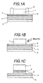
- Figs. 1A, 1B, 1C show illustration views which are viewed from a floating surface of the recording head which is used the high resistivity film for one part of the lower part magnetic film.
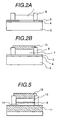
- Figs. 2A, 2B show illustration views which are viewed from a floating surface of the recording head which is used the high resistivity film for one part of the upper part magnetic film.
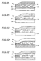
- Figs. 3A, 3B, 3C show illustration views which are viewed from a floating surface of the recording head which is used the high resistivity film for one part of the upper part magnetic film.
- Fig. 4 shows a illustration view which is viewed from a floating surface of the recording head which is used the high resistivity film for one part of the upper and lower part magnetic films.
- Fig. 5 shows a illustration view which is viewed from a floating surface of the recording head which is used the high resistivity film for one part of the upper and lower part magnetic films.
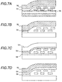
- Figs. 6A, 6B, 6C, 6D, 6E are sectional views which are viewed perpendicularly to a floating side of the recording head which uses a high resistivity film and a high saturation flux density film for one part of the magnetic pole.
- Figs. 7A, 7B, 7C, 7D are sectional views which are viewed perpendicularly to a floating side of the recording head which uses a high resistivity film for one part of the magnetic pole.
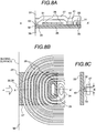
- Figs. 8A, 8B are conception diagrams which show magnetic head in the present invention.
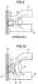
- Fig. 9 is an illustration view to show a problem in a conventional magnetic head.
- Fig. 10 is an illustration view to show effect of the present invention.
- Fig. 11 are shematic views of the the magnetic pole configuration viewed from a sliding surface side of the conventional magnetic head.
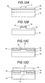
- Figs. 12A, 12B, 12C, 12D are views for showing a manufacture process for manufacturing a main part of the magnetic head in the present invention.
- Fig. 13 is a view for showing a manufacture process for manufacturing a main part of the magnetic head in the present invention.
- Figs. 14A, 14B show a recording reproducing head which is used the high resistivity film or the high saturation flux density film for one part of magnetic pole.
- Fig. 15 is a perspective view of a magnetoresistance effect element sensitive portion of a spin valve type magnetic head relating to the present invention.
- Fig. 16 is a constitution view of the spin valve film which used chrome - manganese alloying film /NiFe in the present invention.
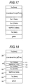
- Fig. 17 is a constitution view of the spin valve film which used chrome - manganese alloying film /Co in the present invention.
- Fig. 18 is a constitution view of a spin valve magnetoresistance effect film used in the present invention.
- Fig. 19 shows a magnetic disc unit using a recording reproducing head in the present invention.
- Figs. 1A, 1B, 1C to Fig. 5 show the structures near recording head portions of magnetic heads seeing from a floating surface. Under an upper shield film 5 there is an MR film or a GMR film which becomes a regenerating head portion.
- the substrate is not specially limited, but it is preferable that the substrate has a small surface roughness (smaller than 5 nm).
- a film of high specific resistance (above 80 ⁇ cm), Bs>1.5 T and magneto-striction (absolute value) ⁇ 1X10 -7 is formed in a portion of the lower magnetic film by the sputtering method, and a non-magnetic film having a thickness of 0.1 to 0.2 ⁇ m is formed thereon by the sputtering method to be used as the gap film 4.
- a high specific resistance film can be obtained by adding oxygen or nitrogen to an Fe, an FeCo or an FeNiCo alloy and also adding an element having a strong affinity with oxygen or nitrogen at the same time.
- the magneto-striction constant can be controlled by adding the other alloy elements, and also depends on concentration of oxygen or nitrogen. Further, a base 3 for plated film is formed on the high specific resistance film by the sputtering method.
- This base 3 may be a high specific resistance film and the film thickness is thinner than 100 nm.
- Resist frames 2 are formed on the base 3, and the upper magnetic film is formed by the plating method.
- the track width is determined by the distance between the frames, and it has been confirmed that the upper magnetic film can be manufactured in 0.5 ⁇ m thickness without composition variation through the frame plating method, and a head having a track width of 0.5 to 1.5 ⁇ m has been manufactured.
- a resist frame is manufactured by masking with an oxide such as SiO 2 through the RIE (reactive ion etching) method. In the frame plating method, it is an alloy film formed of the main component of Fe, NiFe, CoFe or CoNiFe having a specific resistance smaller than 60 ⁇ cm.
- the structure shown in Fig. 5 by forming a part of the upper magnetic film manufactured through this plating method by a high specific resistance film. Further, the side fringe can be reduced by removing the base 3 and the gap film 4 and a part of the lower magnetic film (the upper shield film of MR or GMR) without reattaching through the milling method or the RIE method with masking by the upper magnetic film 1. In a case of using the RIE method, it is possible to etching nearly vertically with masking by the upper magnetic film by optimizing the kind of gas, the gas pressure and the etching rate.
- the recording performance at high frequency can be suppressed to be degraded.
- the film thickness of the upper magnetic film is 2 to 3 ⁇ m, and it is difficult to form all of the upper magnetic film by a high specific resistance plated film. The reason is that the plating bath is difficult to be controlled since a plated film satisfying all the characteristics has a large film stress and consequently various kinds of additives for high resistance and an additive agent for stabilizing the plating bath are used, and that the magneto-striction is more difficult to be adjusted than in the sputtering method.
- the films in the upper side and in the lower side (the upper magnetic film 1 and the lower magnetic film 5) of the gap 4 are manufactured by the plating method, and the high specific resistance film 12 is manufactured on a part of the frame and on the upper magnetic film 1 by the sputtering method.
- the gap film is a conductive non-magnetic film (made of a Cr alloy or the like).
- the frame is made of an oxide such as SiO , and there is no frame removing process as shown in FIG. 1, and accordingly the frame remains on the floating surface as it is. Further, the height of the frame may be a value near the thickness of the upper magnetic film 1.
- the thickness of the upper magnetic film 1 and the lower magnetic film 5 is thinner than 3 times of the thickness of the gap film.
- the frame is formed by an oxide such as SiO , and a low specific resistance ferromagnetic film is formed as the upper magnetic film through the plating method, and further the high specific resistance film 12 is formed on a part of the frame and on the upper magnetic film 1 through the sputtering method as similar to in Figs. 3A, 3B, 3C.
- the width of the lower magnetic film 5 is wider than the width of the upper magnetic film 1 (the track width)
- the side fringe becomes larger than in the other methods.
- the structure of Fig. 4 is similar to that of Fig. 1, but a thin high specific resistance film 12 is also formed on the gap 4 by plating method.
- the film thickness is 0.5 to 3 times as thick as that of the gap. When the film thickness is within this range, effect of high specific resistance can clearly appear in the recording performance and it can be manufactured by the plating method.
- the high specific resistance plated film 12 is a ferromagnetic allot film containing elements such as P, B, O and so on. Further, as shown in FIG. 5, it is possible that a part of an upper shield film 11 and a part of the upper magnetic film 12 are formed by high specific resistance (above 80 ⁇ cm) film through the sputtering method.
- Fig. 5 is a configuration of the recording head looked at from the floating side, and the configuration of the surface which cuts off this head in a vertical direction from floating side is shown in Fig. 6E.
- the lower part magnetic pole and the upper part magnetic pole are constructed to be a multilayer configuration, and top and bottom magnetic films 13,14 that came in contact with the gap membrane 5 may be provided by the galvanizing method.
- the top and bottom magnetic film 13,14 are the membranes added 3d transition metal chemical element to NiFe alloying, CoNiFe- (Pt, Pd) alloying or alloying thereof.
- the gap membrane may be made using flame same as top and bottom magnetic film.
- Magnetism characteristic of top and bottom magnetic films 13,14 are Bs of more than 1.0 T, resistivity of less than 60 ⁇ cm, Hk of less than 20 Oe and magnetostriction constant (lambda) of 1 ⁇ 10-5 or less.
- Film thickness of the top and bottom magnetic film 13,14 is 3 times or more of the gap membrane respectively, and the film thickness of the gap membrane is 0.1 ⁇ m.
- the gap membrane is made of non-magnetic electrical conduction membrane such as CrNi alloying, CuCr alloying, NiW alloying or noble metal membrane.
- High resistivity magnetic film 11,12 may be provided by a suputtering method, and it is a laminating layer of NiFe and Al 2 O 3 membrane, a mixed layer of NiFe membrane and Al 2 O 3 membrane, or a mixed layer of NiFeN and Al 2 O 3 or a multilayer membrane of NiFeN and Al 2 O 3 , thereby composition and membrane constitution thereof are controlled so that the resistivity of the membrane becomes to be higher than that of the top and bottom magnetic film 13,14.
- the saturation flux density ofthe membrane falls and becomes smaller than that of the top and bottom magnetic film made by the galvanizing method. That is, the saturation flux density of the top and bottom magnetic film 13,14 coming in contact with the gap becomes higher than the high resistivity membrane.
- the high saturation flux density membrane had better be disposed to the gap membrane neighborhood as in the embodiment stated above.
- the film thickness of the high resistivity membrane 12 is about 3 ⁇ m.
- the width of the high resistivity upper part magnetic film 12 and the high resistivity lower part magnetic film 11 is larger about 0.5 to 1 ⁇ m than the membrane of the top and bottom magnetic film 13,14, and the width of the top and bottom magnetic film is about 0.5 ⁇ m.
- the regist flame is used and the regist is removed after the galvanizing, and a part except the top and bottom magnetic film 13,14 is covered with protective film (Al 2 O 3 and SiO etc.), and a high resistivity hard magnetism membrane of large width is formed on the top and bottom magnetic film and the protective film.
- a coil consists of two layers in Fig. 6E, however one layer is capable to be used.
- FIG. 6A, 6B, 6C, 6D, 6E A sectional view in a vertical direction of a sliding surface of the recording head is shown in Figs. 6A, 6B, 6C, 6D, 6E.
- Figs. 6A, 6B, 6C, 6D, 6E respectively show sectional views corresponding to Figs.1A, 1B, 1C, Fig. 2A, 2B, Fig. 3A, 3B, 3C, Fig. 4, Fig. 5.
- the upper part magnetic film consists one layer of the magnetic film
- the lower part magnetic film consists of two layers of the magnetic films
- the magnetic film near the gap membrane 56 of the lower part magnetic film is high resistivity membrane.
- the coil 55 is disposed between the insulation membranes on the gap membrane 56, and the magnetic field is generated from the floating side by flowing an electric current in the coil.
- the lower part magnetic film consists one layer of the magnetic film
- the upper part magnetic film consists of two layers of the magnetic films
- the magnetic film near the gap membrane 56 of the upper part magnetic film is high resistivity membrane is a high saturation flux density low resistivity membrane 51.
- the high saturation flux density low resistivity membrane makes it with gilt method is made by the galvanizing method and width of the magnetic film defines the track width.
- the high saturation flux density low resistivity membrane is formed only by the floating side of the upper part magnetic film, and the width of the high saturation flux density low resistivity membrane viewed from the floating side is narrower than the high resistivity magnetic film 52 as to shown in Fig. 2.
- the configuration shown in Fig. 6B is more suitable to construct narrow track easily than the configuration shown in Fig. 6A.
- the lower part magnetic film and the upper part magnetic film consist of two layers of the magnetic films.
- the lower part magnetic film consists of the high saturation flux density low resistivity membrane 51 and the hard magnetism membrane 54 thereunder, and the upper part magnetic film consists of the high saturation flux density low resistivity membrane 51 and the high resistivity magnetic film 52.
- the high saturation flux density low resistivity membrane 51 and the gap membrane 56 are made by the galvanizing method, and the high resistivity magnetic film 52 is made by the suputtering method.
- the saturation flux density low resistivity membrane is used on and under the gap membrane 56, the width viewed at from the floating side may be made narrower than the width of other magnetic films, it is a configuration effective for recording head having the narrow track, and the high saturation flux density membrane is used for the gap neighborhood. Therefore, the magnetic field strength becomes higher, and radio frequency characteristic is good, too as using the magnetic film of high resistivity.
- Fig. 6D shows the high saturation flux density membrane 51 forming the whole magnetic pole on and under the gap membrane 56.
- Fig. 6E shows a similar configuration as Fig. 6C, and the high saturation flux density low resistivity membrane is used to came in contact with gap membrane 56, and the high resistivity magnetic film 52 is used for the magnetic pole material apart from and over and under the gap, and the radio frequency characteristic thereof is excellent, and the track width is capable to be less than 1.0 ⁇ m.
- the high saturation flux density low resistivity membrane 51 has higher saturation flux density than that of the magnetic pole material used for other parts in each recording head, and the resistivity thereof is smaller than that of the material of other magnetic pole parts.
- the material used for the high saturation flux density low resistivity membrane 51 for example, CoNiFe alloying, NiFe alloying or the material which added 3d transition metal chemical element in these alloying are used.
- the non-magnetic electrical conduction membrane when making it by galvanising method oxide such as Al 2 O 3 or SiO 2 when making it by other methods, or even nitride, carbide or any mixing material thereof may be used.
- Configuration examples of the recording head which is similar to the configurations of Fig. 6A, Fig. 6B, Fig. 6C, Fig. 6D, Fig. 6D are shown in , Fig. 7B, Fig. 7C, Fig. 7D.
- a magnetic film is provided on and under the gap membrane 56 and apart therefrom as the high resistivity magnetic film 52, the hard magnetism membrane 54 having smaller resistivity than that of the high resistivity magnetic film 52 is disposed in the magnetic gap side.
- the volume of the high resistivity magnetic film 52 is larger than the volume of the hard magnetism membrane 54 having the low resistivity, and the radio frequency characteristic is improved than that in the case that there is not using the high resistivity membrane.
- the magnetic film which cames in contact with a gap membrane and other gap membrane is formed with the narrow track,and the magnetic film thereon is constructed with the high resistivity magnetic film 52, thereby good recording head of narrow track and radio frequency characteristic may be offered.
- the upper part magnetic film consists three layers, the gap membrane 56 is made at a flat part, the magnetic film that width is narrow is provided thereon, and the high resistivity magnetic film 52 is formed through the magnetic film.
- the hard magnetism membrane 54 having the low resistivity is provided on the high resistivity magnetic film 52, the magnetic field strength of the floating side is capable to be high by making the saturation flux density of the hard magnetism membrane 54 having this low resistivity, higher.
- the configuration resembled to Fig. 7C is a recording head shown in Fig. 7D, and the upper part magnetic films consists of the three laiyers the hard magnetism membrane 54 of the low resistivity is provided on a part near the gap membrane 56 and the high resistivity magnetic film 52 is provided on a part being far from the gap membrane, thereby the saturation flux density of the material of the gap neighborhood is capable to be higher than that in Fig. 7C, and the head that the magnetic field strength is high may be offered.
- Fig. 8 A shows a section of the magnetic head having new configuration in the present invention.
- a coil 26 is provided between the lower part core 25 and the upper part core 27, and consists of Al or Cu of thickness 2 ⁇ m.
- An insulating material 31 of the non-magnetism is filled up with an object to maintain the electric insulation with the coil 26 and cores 25,27.
- a coil 26 is enveloped between the lower core 25 and the upper core 27.
- the coil 26 is formed of an Al or Cu film having thickness of 2 ⁇ m.
- a non-magnetic and insulating material 31 is filled between the coil 26 and the cores 25, 27 to electrically insulate between them.
- the magnetic head in accordance with the present invention is characterized by that magnetic pole members 32, 33 and an insulating and non-magnetic film 10 are inserted between the upper core 27 and the lower core 25, and a magnetic gap (or recording gap) is formed by these members. Further, another characteristic point is that magnetic path members 41, 42 are provided between the upper core 27 and the lower core 25. This structure is not a necessary structure to realize the present invention.
- the magnetic path members 41, 42 are preferable to flatten the upper core 27, and have an effect to reduce stress (magneto-striction) remaining after manufacturing. By forming the members together with the magnetic pole members 32, 33, increase in manufacturing cost can be prevented.
- Fig. 8B is a view showing the magnetic head seeing from the upper core side. It can be understood that the coil 26 is wound in a spiral shape. The coil 26 is connected to an electrode 30 (Fig. 8A) in a contact hall 34. Further, the upper core 27 and the lower core 25 are connected in a magnetic contact hall 35. The magnetic contact hall 35 is constructed including the magnetic path members 41, 42 described above.
- the insulating and non-magnetic film 10 characterized by the present invention is placed at a position in the ends of the upper core 27 and the lower core 25, and the structure of the members seeing from the direction ⁇ is as shown by the Fig. 8C. That is, the magnetic pole members 32, 33 having a narrow width are interposed between the upper core 27 and the lower core 25, and further the insulator non-magnetic film 10 is placed between the members.
- the magnetic pole members 32, 33 are magnetically integrated with the ends of the magnetic poles of the upper core 27 and the lower core 25, respectively. Therefore, the gap portion is formed by the magnetic poles respectively having the projecting portion.
- Fig. 8C agrees with the magnetic pole structure seeing from a plane of the magnetic head accessing to the recording medium, and it can be understood from the figure that the upper magnetic pole has a projecting shape and the projecting portion is formed toward the lower magnetic pole.
- both of the magnetic poles have a projecting shape, and particularly the width of the projecting portion of the upper magnetic pole is nearly equal to the width of the projecting portion of the lower magnetic pole.
- the height of the projecting portion is set to approximately 0.8 ⁇ m, and the width of the projecting portion is set to approximately 1 ⁇ m. From this relationship, the height of the projecting portion is lower than the width of the projecting portion.
- the structure disclosed by the present invention can be reduced the resistance of the magnetic path as the same as that of Japanese Patent Application Laid-Open No.7-296328. Description will be made, referring to Fig. 9.
- the figure is a cross-sectional view of a conventional magnetic head which does not have the magnetic pole members 32, 33.
- the figure shows the magnetic gap put between the lower core 25 and the upper core 27.
- Writing-in magnetic flux to a medium 61 is conducted as a path indicated by ⁇ .
- the width of the gap (magnetic pole width) of the end side of the upper core 27 is narrowed, the magnetic path resistance is increased and by this effect the magnetic flux becomes to flow through a path indicated by ⁇ in a region 50 where the magnetic path resistance is increased.
- an amount of the magnetic flux conducted to the gap end portion 51 is decreased and a necessary amount of magnetic flux cannot be extracted from the gap (magnetic pole) ends.
- the path ⁇ can be increased by thickness of the members (the non-magnetic region can be widened). By this effect, it is possible to suppress the amount of magnetic flux flowing through the path ⁇ even if the magnetic path resistance is increased by narrowing the width of the magnetic poles.
- the above-mentioned effect can be observed in a writing-in frequency above 150 MHz.
- the writing-in frequency can be increased up to 200 MHz.
- the width w1 of the magnetic pole members 32, 33 is narrower than the width of the upper magnetic pole 27 and the width of the lower magnetic pole 25. This is the base that the magnetic pole has the projecting portion.
- the magnetic flux is concentrated in the projecting portions opposite to each other. Therefore, under a condition that the magnetic field from the projecting portion is adjusted so as to agree with the magnetic field necessary writing-in by adjusting the coil current (writing-in current), writing cannot occur in the region except for the projecting portion (in the region where the gap dimension becomes wide). Therefore, track width to be written can be brought to agree with the width of the projecting portion.
- only the projecting portions may be made of a high electric resistance and high saturation magnetizing material, and thereby a strong magnetic field can be generate in the region corresponding to the width of the projecting portion.
- the writing-in track width can be efficiently limited to the width of the projecting portion even if the magnetic pole has the projecting shape.
- the width of the projecting portion can be made smaller than 2 ⁇ m by a process to be described later. By this effect, the width of writing in a medium can be easily reduced to 2 ⁇ m or smaller.
- the width of writing-in is determined by the width of the projecting portion, there is no need to particularly narrow the width of the upper core 27 and the width of the lower core 25 in order to realize high density recording. By this effect, the necessary magnetic field can be efficiently conducted to the magnetic pole end portion (the gap portion) without increasing the magnetic path resistance.
- the shapes of the magnetic heads can be roughly classified into three kinds as shown in Fig. 11 when the magnetic poles are seen from the sliding surface side. That is, they are a magnetic head constructed by magnetic poles 27, 25 having different length as shown by Fig. 11A, a magnetic head constructed by magnetic poles 27, 25 having the same length as shown by Fig. 11B, and a magnetic head having a projection in one of the magnetic poles 25.
- the magnetic head Fig. 11B is an improved one of the magnetic structure of Fig. 11B, and has a characteristic of small magnetic field leakage in the track width direction since the lengths of the magnetic poles are equal to each other.
- this structure has a disadvantage in that the magnetic pole 25 cannot be also used as a shield layer to a magneto-resistance effect element.
- a countermeasure of the disadvantage is the structure shown in Fig. 11C.
- the width W In order to realize the narrow track in the structure shown in Fig. 11C, the width W needs to be narrowed. Therefore, the writing-in magnetic flux is decreased due to increase of the magnetic path resistance shown in Fig. 9. Accordingly, it is impossible to write high density information at a high efficiency.
- the width of the writing-in gap portion is limited by the width of the projection portion, spreading of the leakage magnetic field toward the track width direction is small as similar to in the magnetic poles shown in Fig. 11B. Therefore, the structure in accordance with the present invention is suitable for high density recording. Further, since the width of the lower core is wider than the width of the projecting portion, there is no problem in that the lower core is also used as a shield layer to a magneto-resistance effect element.
- the magnetic head structure in accordance with the present invention has no problems in connection to high density recording which are problems in the conventional magnetic head.
- a manufacturing process of the magnetic head capable of realizing the excellent performance will be described below, referring to Fig. 12.
- FIG. 8B shows features of forming the end of magnetic pole of the magnetic core seeing from the direction " ⁇ " shown in Fig. 8B.
- the processes will be sequentially described below, referring to the figure.
- a magnetic film 73 composing the lower magnetic pole is laminated on a substrate (or a base layer or a base structure) 74.
- a Ni-Fe alloy is used as the magnetic film.
- the thickness is set to 2 ⁇ m.
- an alumina film 72 having a thickness of 0.3 ⁇ m as an insulator non-magnetic film is laminated and further a Ni-Fe magnetic alloy film 72 having a thickness of 0.8 ⁇ m is laminated.
- a resist pattern 71 having a width of the projecting portion (corresponding to the writing-in track width) is formed through a photolithographic method. The thickness is set to 1 ⁇ m.
- the magnetic alloy film 72 is etched by an ion milling method with masking of the resist pattern 71 to form a portion to be formed in the projecting portion of the upper magnetic pole.
- the alumina film is etched by a chlorine and fluorine reactive gas with masking of the resist pattern 71 and the projecting portion of the upper magnetic pole formed by the etching.
- a projecting portion is formed in the lower magnetic pole by etching the lower magnetic pole through the ion milling method with masking of the member to be formed in the projecting portion of the upper magnetic pole.
- the depth of the etching is set to 0.8 ⁇ m.
- thermo-curing insulator used in manufacturing of semiconductors (so-called spin-on-glass), and performing the necessary heat treatment, and then mechanically lapping the surface of the substrate.
- spin-on-glass a fluid thermo-curing insulator used in manufacturing of semiconductors
- thermo-fluidity of the resist it is possible to use thermo-fluidity of the resist.
- the member 72 to form the projecting portion is exposed from the insulator layer. If a process can realize the necessary condition, the flattening process of the insulator layer is not required. For example, even if the thickness of the insulator member 76 exceeds the thickness of the member 72 to be formed in the projecting portion, it has been confirmed that the present invention is not affected. In such an extreme case (a condition where the thickness of the insulator member 76 exceeds the thickness of the member 72 to be formed in the projecting portion), an undulation is produced in the upper magnetic pole and it results in that the projecting portion exists in the depressed portion. This structure is to be described in another part.
- the other members composing the upper magnetic pole member is formed.
- a Ni-Fe alloy film is used for the upper magnetic pole as the same as in the conventional magnetic head.
- the magnetic structure shown in Fig. 8C can be formed.
- the NI-Fe alloy film is used for the material for the magnetic pole in this embodiment
- the magnetic head in accordance with the present invention can be formed by using the other soft magnetic film through the same process as in this embodiment. Particularly, by using a high electric resistant soft magnetic film, writing-in under a high frequency condition can be realized. It is a characteristic of the present invention that the soft magnetic film can be formed depending on the eletroplating method, and by this effect it is possible to perform writing at a high frequency exceeding that of the conventional magnetic head.
- a structure of the upper magnetic pole having a depressed portion will be described below.
- the structure can be manufactured through processes of manufacturing a magnetic head including at least the following process. Description will be made, referring to Fig. 12 as similar to the previous explanation.
- an insulator non-magnetic film 75 is laminated and further a material 72 composing a part of the upper magnetic pole is laminated.
- a resist pattern 71 is formed in a region corresponding to the projecting portion of the upper magnetic pole through a lithographic method.
- a projecting portion is formed in the lower magnetic pole by etching the insulator non-magnetic film and the lower magnetic pole with masking of the resist pattern 71 and the member to be formed in the projecting portion of the upper magnetic pole.
- a non-magnetic and insulating film 76 with a thickness exceeding the projecting portion is laminated over the region except for the projecting portion.
- the thickness of the insulator non-magnetic film 76 exceeds the surface of the projecting portion (the surface of 72).
- the objective magnetic pole shape of the magnetic head is manufactured.
- Fig. 13 shows the magnetic pole shape of the magnetic head manufactured through the manufacturing processes including at least the above-mentioned process.
- the figure clearly shows the shape of the upper magnetic pole 77 having the projecting portion in the depressed portion.
- the magnetic head in accordance with the present invention is formed on a wafer obtained by machining a sintered body of alumina and titanium carbide. Then, after performing desired machining, a magnetic head slider is manufactured.
- the width of the projecting portion determining the writing-in track width is determined by the width of the resist pattern.
- a resist pattern having a thick film thickness is not always necessary. From this effect, patterning resolution is easier compared to the resist pattern of a plating mask pattern, and the width of the projecting portion can be made smaller than 2 ⁇ m. By this characteristic, a magnetic head used for narrow track can be easily manufactured.
- Fig. 14 shows an example of a recording reproducing head in which the high resistivity membrane as shown in the embodiment 1 is used for the recording head and the recording head is combined with a reproducing head as shown in the following.
- a huge magnetoresistance effect membrane 104 is used for the reproducing head, an electrode 105 to flow an electric current contacts with the huge magnetoresistance effect membrane 104 electrically.
- a high resistivity lower part magnetic film 108 is disposed as the upper part shielding membrane through the upper part gap membrane on the huge magnetoresistance effect membrane 104, and the high resistivity lower part magnetic film 108 consists of one part of the lower part magnetic pole of the recording head.
- the radio frequency characteristic of the recording head may be improved.
- the width of the gap membrane 102 of recording head is equal to that of the magnetic films disposed on and under the addition, and the high saturation flux density membranes 101,103 on and under the gap are desirable to be constructed with a material of higher saturation flux density than that of other magnetic pole parts.
- a high resistivity upper part magnetic film 107 having a larger width is used on this high saturation flux density membrane 101.
- An electric current is flown in the coil 109 of the recording head, and the recording media 110 is recorded by a magnetic field from the recording head.
- a head of the different configuration used to a hard magnetism tunnel membrane may be used for the reproducing head.
- Fig. 15 is a partial sectional view of the magnetic head (MR sensor) using a spin valve magnetoresistance effect membrane in the present invention.
- MR sensor in the present invention has a configuration which sticks the second magnetic layer 22 of first magnetic layer 45 of soft ferromagnetic body, non-magnetic metal layer 21 and ferromagnetic body, on an appropriate substrate 43 as glass or ceramic.
- Magnetization direction of the second magnetic layer 22 is fixed to the same direction as a magnetic field direction of the magnetic media.
- the magnetization direction of the first magnetic layer 45 of the soft ferromagnetic body when the magnetic field is not applied inclines 90 degrees to the magnetic field direction of the second magnetic layer.
- a magnetization rotation occurs with the first magnetic layer 45 responding to the applied magnetic field.
- the first magnetic layer 45, the non-magnetic metal layer 21, the second magnetic layer 22 and the antiferromagnetic substance layer 23 explained in the embodiment of the present invention are capable to use a membrane constitution as the laminating configuration shown by later Fig. 16, Fig. 17 and Fig. 18, and moreover as the hard magnetism layer 47, Co 82 Cr 9 Pt 9 , Co 80 Cr 8 Pt 9 (ZrO 2 ) 3 may be used.
- FIG. 16, Fig. 17 and Fig. 18 show the first magnetic layer 45 in this embodiment and a membrane constitution equivalent to the second magnetic layer 22 and those magnetic field directions are formed same as the said article.
- an appropriate lower part membrane 24, for example, such as Ta, Ru or CrV is stuck on a substrate 43.
- An object to stick the lower part membrane 24 is in optimizing formation, grain size number and a form of the layer stuck later.
- the form of the layer is very important to get suitable MR effect. Furthermore, it is because the a very thin distance piece layer of the non-magnetic metal layer 21 may be utilized by the formation of the layer.
- a high electric resistance is preferable to be used as the lower part layer.
- the lower part layer may be used as a reverse configuration as mentioned above.
- Substrate 43 is made of a sufficient high electric resistance and a plane fully and in case of appropriate crystal structure, the lower part membrane 24 is unnecessary.
- first magnetic layer 45 means for producing a bias in a londitudinal direction is used in order to maintain a single domain condition in a direction to be parallel to this page.
- a rigid hard magnetism layer 47 having characteristics of high saturation coercive force, high right angle degree, high electric resistance is used as well.
- the rigid hard magnetism layer 47 contacts with a domain of an end of the first magnetic layer 45 made of the soft ferromagnetic body.
- Magnetization direction of the rigid hard magnetism layer 47 is parallel to this page.
- the first antiferromagnetism layer contacts with the domain of the end of the magnetic layer 45 so as to be stuck, and a necessary bias in a londitudinal direction occurs.
- the antiferromagnetism layer is preferrable to have a blocking temperature which is sufficientry different from that of an antiferromagnetism layer 23 which is used in order to let the magnetization direction of the second magnetic layer 22 made of the ferromagnetic body, fixed.
- a capping layer made of the high resistance such as Ta, for example, is desirable to be stuck on all of the upper part of the MR sensor.
- An electrode 28 is provided, and a circuitry is formed between the MR sensor structure, the current source and the detection means.
- Fig. 16 to Fig. 18 respectively show a membrane constituting a magnetoresistance effect element in the present invention formed in stead of each membrane of the non-magnetic metal layer 21, the second magnetic layer 22 and the antiferromagnetic substance layer 23 shown in Fig. 15, and it is formed by a radio frequency magnetron suputtering apparatus as follows.
- tantalum, nickel -20at % ferrum alloying, copper, cobalt, chrome -50at % manganese are used.
- a chrome - manganese alloying membrane a chip of 1 cm ⁇ 1 cm of an additional element is arranged on a chrome - manganese target top, and number of the chip is increased or decreased so as to adjust the composition thereof.
- Co-Fe-Ni layer is made as the hard magnetism membrane, the chip of 1 cm ⁇ 1 cm of nickel, ferrum is arranged on the cobalt target top to adjust the composition.
- Each layer of the laminating film is formed successively by generating Plasma in the apparatus by applying a radio frequency electric power on the cathode arranging each target, and opening and shutting a shutter arranged in every each cathode.
- a laminating film is heat-treated in a vacuum thermal treatment equipment after being formed.
- the heat treatment is performed by raising the temperature up from the room temperature a predetermined temperature, for example 250 °C, and after holding the temperature for a predetermined time, for example one hour, cooling off to a room temperature.
- the magnetic field from 2 to 5 k Oe is applied in parallel to the surface of the substrate.
- a direction of the above magnetic field is parallel to the magnetic field applied by the permanent magnet when forming the film.
- Formation of the element on the substrate is performed by a photo resist production process.
- the substrate is processed by a slider, and is loaded in the magnetic recording apparatus.
- Fig. 16 is a figure comparing characteristics before the heat treatment and after the heat treatment the spin valve film which has the magnetic laminating body using the antiferromagnetism film of 45 at % chrome -45 at % manganese -10 at % platina/81 at % Ni-19 at % Fe film.
- the coupling magnetic field by one direction anisotropism appear as a shift quantity of a right side loop of the figure.
- the coupling magnetic field before heat treatment is 300 Oe, 250 °C, and 380Oe after the heat treatment of three hours. Considering the thickness of Ni Fe layer and the size of the magnetization, it is same size with the dimension shown in the prior art.
- Fig. 17 is a figure comparing characteristics before the heat treatment and after the heat treatment of the spin valve film which has the magnetic laminating body using the antiferromagnetism film of 45 at % chrome -45 at % manganese -10 at % platina/ Co film.
- the coupling magnetic field before the heat treatment is almost similar to that in the case shown in Fig. 1 with 300 Oe, after the heat treatment for three hours in 250 °C, the coupling magnetic field becomes 600 Oe, about two times than before. Considering the thickness of the Co layer and the size of the magnetization, it is size of about two times of the coupling magnetic field shown by Fig. 1.
- Fig. 18 is an other constitution example in the present invention using a magnetic laminating body as the spin valve magnetoresistance effect film,
- the antiferromagnetism film 30 (45 at % Cr-45 at % Mn-10 at % Pt) and the hard magnetism layer 65 sticking thereto respectively consist of a Co layer 111 directly connected to the antiferromagnetism film 30, the soft magnetism layer 112 having a good magnetism characteristic (81 at % Ni-19 at % Fe), and a Co layer 113 directly contacting with the non-magnetic layer 62 (Cu) and producing huge magnetoresistance effect.
- a foundation film 64 is the foundation layer for controlling orientation and crystal grain size of other film, and a soft magnetism layer 63 (81 at % Ni-19 at % Fe) is a free layer.
- the Co layer is arranged at a joint portion with the antiferromagnetism film and a jointportion with the non-magnetic film, however the magnetism characteristic of the hard magnetism layer 65 as the fixed layer is not deteriorated, and thickness and characteristic of the hard magnetism layer 65 may be held without increasing the magnetization quantity of the total layer.
- the soft magnetism layer 112 is desirable to have a good magnetism characteristic and to have a smaller saturation flux density than those of the layers 113 and 111 consisting of Co, for example, Ni 81 Fe 19 film of the saturation flux density of 1 Tesla.
- the saturation flux density may be fallen to be even 0.5 Tesla or so, and for example, NiFe-Cr film is suitable, too, this NiFe-Cr film consists of NiFe alloying containing 0 to 20 at % Cr, and this NiFe alloying consists of 75-95 at % Ni and remainder Fe.
- Fig. 19 is a total figure of the magnetic disc unit using the recording reproducing sectional pattern head shown in the embodiment 2.
- Recording reproducing separating type magnetic head 201 is controlled a location on a recording media 203 by head positioning frame 202 on the recording media 203 as a magnetic disk turned by a motor, and the recording reproducing separating type magnetic head 201 is connected with a regenerative signal processor 204.
- This apparatus consists of a DC motor for turning the magnetic disk, a magnetic head to write in information and to read it, a positioning apparatus to support the magnetic head and to change a location thereof to the magnetic disk, that is an actuator and voice coil motor, and an air filter to keep the apparatus inside cleanly.
- the actuator consists of a carriage, a rail, and a bearing
- the voice coil motor consists of a voice coil and a permanent magneto.
- Magnetic disk is constructed with a good surface having surface roughness R MAX of 100 ⁇ or less, preferably of 50 ⁇ or less.
- the magnetic disk has the magnetic recording layer formed by a vacuum film formation method on the surface of the hard substrate.
- the magnetic thin film is used for the magnetic recording layer.
- the film thickness of the magnetic recording layer formed by the vacuum film formation method is 0.5 ⁇ m or less, the surface condition of the hard substrate is just reflected as that of the recording layer.
- one having the surface roughness R MAX of 100 A or less is used for the hard substrate.
- glass, chemical strengthen soda-almina silica glass or ceramic are used as a main component thereof.
- the magnetic layer made of metal or alloying it is preferable to provide the oxide layer or nitride layer on the surface, or for the surface with an oxide film. Moreover, use of carbon protective coat is desirable, too.
- MR sensor of high sensitivity having excellent MR effect based on the anisotropism magnetoresistance effect, such as media transfer rate 15MB/second or greater, recording frequency 45 MHz or more, high-speed transmitting of the data more than magnetic disk 4000 rpm, abbreviation of access time, increase of recording capacity, thereby, a magnetic disc unit with 3Gb/ in 2 or greater is provided as surface recording density.
- At least one part of the magnetic pole of the recording head is made of high resistivity film, and as the recording performance is hard to fall in the radio frequency, a magnetic storage apparatus of high recording density is provided.
- a magnetic laminating body which had a sufficient coupling magnetic field and a high temperature stability may be provided, thereby, a reproducing head which has a sufficient reproducing capacity and low noise characteristic and a high density magnetic storage apparatus of high reliability may be provided.
Landscapes
- Engineering & Computer Science (AREA)
- Chemical & Material Sciences (AREA)
- Nanotechnology (AREA)
- Manufacturing & Machinery (AREA)
- Crystallography & Structural Chemistry (AREA)
- Physics & Mathematics (AREA)
- Mathematical Physics (AREA)
- Theoretical Computer Science (AREA)
- Metallurgy (AREA)
- Electromagnetism (AREA)
- Thin Magnetic Films (AREA)
- Magnetic Heads (AREA)
Applications Claiming Priority (6)
| Application Number | Priority Date | Filing Date | Title |
|---|---|---|---|
| JP34494196 | 1996-12-25 | ||
| JP344995/96 | 1996-12-25 | ||
| JP344941/96 | 1996-12-25 | ||
| JP34499596 | 1996-12-25 | ||
| JP34494196 | 1996-12-25 | ||
| JP34499596 | 1996-12-25 |
Publications (3)
| Publication Number | Publication Date |
|---|---|
| EP0851411A2 true EP0851411A2 (de) | 1998-07-01 |
| EP0851411A3 EP0851411A3 (de) | 1998-09-16 |
| EP0851411B1 EP0851411B1 (de) | 2004-10-13 |
Family
ID=26577918
Family Applications (1)
| Application Number | Title | Priority Date | Filing Date |
|---|---|---|---|
| EP97122699A Expired - Lifetime EP0851411B1 (de) | 1996-12-25 | 1997-12-22 | Dünnschicht-Magnetkopf und magnetisches Aufnahme/Wiedergabe-Gerät |
Country Status (5)
| Country | Link |
|---|---|
| US (1) | US6034847A (de) |
| EP (1) | EP0851411B1 (de) |
| KR (1) | KR100319035B1 (de) |
| DE (1) | DE69731177T2 (de) |
| SG (1) | SG55435A1 (de) |
Cited By (2)
| Publication number | Priority date | Publication date | Assignee | Title |
|---|---|---|---|---|
| EP0881627A2 (de) * | 1997-05-27 | 1998-12-02 | TDK Corporation | Dünnfilmmagnetkopf |
| WO2001059768A2 (en) * | 1999-10-05 | 2001-08-16 | Seagate Technology Llc | High data rate writer poles |
Families Citing this family (38)
| Publication number | Priority date | Publication date | Assignee | Title |
|---|---|---|---|---|
| JPH10340430A (ja) * | 1997-06-10 | 1998-12-22 | Fujitsu Ltd | スピンバルブ磁気抵抗効果型ヘッドおよび磁気記憶装置 |
| SG68063A1 (en) * | 1997-07-18 | 1999-10-19 | Hitachi Ltd | Magnetoresistive effect type reproducing head and magnetic disk apparatus equipped with the reproducing head |
| US6510024B2 (en) | 1998-06-30 | 2003-01-21 | Fujitsu Limited | Magnetic head and method of manufacturing the same |
| JP3755560B2 (ja) * | 1998-06-30 | 2006-03-15 | 富士通株式会社 | 磁気ヘッド及びその製造方法 |
| JP3721262B2 (ja) * | 1998-07-23 | 2005-11-30 | 株式会社日立グローバルストレージテクノロジーズ | 薄膜磁気ヘッドの製造方法および磁気ヘッド |
| US6195240B1 (en) * | 1998-07-31 | 2001-02-27 | International Business Machines Corporation | Spin valve head with diffusion barrier |
| JP2000057520A (ja) * | 1998-08-04 | 2000-02-25 | Hitachi Ltd | 磁気ヘッド及びそれを用いた磁気記憶装置 |
| JP2000113437A (ja) * | 1998-10-08 | 2000-04-21 | Read Rite Smi Kk | 磁気ヘッド装置の製造方法、磁気ヘッド装置、並びに、磁気ヘッド装置の中間製造物 |
| JP2000207707A (ja) * | 1999-01-08 | 2000-07-28 | Hitachi Ltd | 薄膜磁気ヘッド及びこれを用いた磁気ディスク装置 |
| US6765756B1 (en) * | 1999-03-12 | 2004-07-20 | Western Digital (Fremont), Inc. | Ultra-short yoke and ultra-low stack height writer and method of fabrication |
| JP3455155B2 (ja) * | 1999-06-28 | 2003-10-14 | アルプス電気株式会社 | 薄膜磁気ヘッド及びその製造方法 |
| JP2001060307A (ja) * | 1999-08-24 | 2001-03-06 | Tdk Corp | 薄膜磁気ヘッドおよびその製造方法 |
| JP2001110008A (ja) * | 1999-10-06 | 2001-04-20 | Nec Corp | 磁気ヘッドおよびその製造方法、および磁気記録再生装置 |
| US6417990B1 (en) * | 1999-12-06 | 2002-07-09 | Seagate Technology Llc | Composite core structure for high efficiency writer |
| US7002776B2 (en) * | 1999-12-06 | 2006-02-21 | Tdk Corporation | Thin film magnetic head and method of manufacturing same |
| US6473960B1 (en) | 2000-01-07 | 2002-11-05 | Storage Technology Corporation | Method of making nitrided active elements |
| US6807031B2 (en) | 2000-02-08 | 2004-10-19 | Seagate Technology Llc | Single domain state laminated thin film structure for use as a magnetic layer of a transducing head |
| US6548186B1 (en) | 2000-05-19 | 2003-04-15 | International Business Machines Corporation | High resistivity films for AP layers in spin valves |
| US6539610B1 (en) * | 2000-07-14 | 2003-04-01 | International Business Machines Corporation | Method for manufacturing a magnetic write head |
| US6972932B2 (en) * | 2000-09-06 | 2005-12-06 | Seagate Technology Llc | High-efficiency single-turn write head for high-speed recording |
| US6778357B2 (en) | 2000-11-10 | 2004-08-17 | Seagate Technology Llc | Electrodeposited high-magnetic-moment material at writer gap pole |
| KR100394993B1 (ko) * | 2001-02-20 | 2003-08-19 | 한국과학기술연구원 | FeCoNiN계 연자성 박막합금 조성물 |
| JP4365547B2 (ja) * | 2001-08-20 | 2009-11-18 | 富士フイルム株式会社 | 磁気記録再生方法 |
| AU2002259093A1 (en) * | 2002-01-08 | 2003-07-30 | Seagate Technology Llc | Low saturation induction material for magnetic recording head write pole |
| US7573677B2 (en) * | 2002-03-01 | 2009-08-11 | International Business Machines Corporation | Reduction of interference pickup in heads for magnetic recording by minimizing parasitic capacitance |
| US7688545B1 (en) | 2002-09-11 | 2010-03-30 | Seagate Technology Llc | Recording head writer with high magnetic moment material at the writer gap and associated process |
| JP4183554B2 (ja) * | 2002-09-12 | 2008-11-19 | Tdk株式会社 | 軟磁性膜の製造方法と薄膜磁気ヘッドの製造方法 |
| JP3691833B2 (ja) * | 2003-07-28 | 2005-09-07 | 株式会社Neomax | 薄膜磁気ヘッド用基板およびその製造方法 |
| US7506428B2 (en) * | 2003-09-30 | 2009-03-24 | Hitachi Global Storage Technologies Netherlands B.V. | Ion mill process with sacrificial mask layer to fabricate pole tip for perpendicular recording |
| US7323215B2 (en) * | 2004-05-14 | 2008-01-29 | Headway Technologies, Inc. | Free layer design for CPP GMR enhancement |
| JP2006012250A (ja) * | 2004-06-23 | 2006-01-12 | Tdk Corp | 垂直磁気記録用磁気ヘッド |
| US7354505B2 (en) * | 2004-08-25 | 2008-04-08 | Board Of Trustees Of Michigan State University | Epitaxial ferromagnetic Ni3FeN |
| US7367110B2 (en) * | 2004-09-27 | 2008-05-06 | Hitachi Global Storage Technologies Netherlands B.V. | Method of fabricating a read head having shaped read sensor-biasing layer junctions using partial milling |
| US7431961B2 (en) * | 2004-12-10 | 2008-10-07 | Headway Technologies, Inc. | Composite free layer for CIP GMR device |
| US7821736B2 (en) * | 2006-04-06 | 2010-10-26 | Hitachi Global Storage Technologies Netherlands, B.V. | Shaped trailing shield of a perpendicular recording write element |
| US8259410B1 (en) | 2008-05-23 | 2012-09-04 | Western Digital (Fremont), Llc | Method and system for providing a magnetic head using a composite magnetic material in the recording transducer |
| JP5338711B2 (ja) * | 2010-02-23 | 2013-11-13 | Tdk株式会社 | 磁気センサー、磁気検出装置、及び磁気ヘッド |
| US10247790B2 (en) * | 2015-03-12 | 2019-04-02 | Tdk Corporation | Magnetic sensor |
Citations (5)
| Publication number | Priority date | Publication date | Assignee | Title |
|---|---|---|---|---|
| EP0222183A2 (de) * | 1985-10-14 | 1987-05-20 | Hitachi, Ltd. | Dünnschichtmagnetkopf |
| WO1992016935A1 (en) * | 1991-03-25 | 1992-10-01 | Eastman Kodak Company | Thin film laminated magnetic record/playback head for high bit densities and data transfer rates |
| JPH05120630A (ja) * | 1991-04-25 | 1993-05-18 | Hitachi Ltd | 磁気デイスク装置 |
| US5438747A (en) * | 1994-03-09 | 1995-08-08 | International Business Machines Corporation | Method of making a thin film merged MR head with aligned pole tips |
| EP0678855A1 (de) * | 1994-04-21 | 1995-10-25 | Hitachi, Ltd. | Magnetisches Speichergerät |
Family Cites Families (10)
| Publication number | Priority date | Publication date | Assignee | Title |
|---|---|---|---|---|
| US5126907A (en) * | 1989-05-24 | 1992-06-30 | Hitachi, Ltd. | Thin film magnetic head having at least one magnetic core member made at least partly of a material having a high saturation magnetic flux density |
| US5590008A (en) * | 1991-04-25 | 1996-12-31 | Hitachi, Ltd. | Magnetic disc unit having a plurality of magnetic heads which include multilayer magnetic films |
| US5315468A (en) * | 1992-07-28 | 1994-05-24 | International Business Machines Corporation | Magnetoresistive sensor having antiferromagnetic layer for exchange bias |
| US5301079A (en) * | 1992-11-17 | 1994-04-05 | International Business Machines Corporation | Current biased magnetoresistive spin valve sensor |
| US5343422A (en) * | 1993-02-23 | 1994-08-30 | International Business Machines Corporation | Nonvolatile magnetoresistive storage device using spin valve effect |
| US5465185A (en) * | 1993-10-15 | 1995-11-07 | International Business Machines Corporation | Magnetoresistive spin valve sensor with improved pinned ferromagnetic layer and magnetic recording system using the sensor |
| US5435053A (en) * | 1994-03-02 | 1995-07-25 | International Business Machines Corporation | Simplified method of making merged MR head |
| JP2784431B2 (ja) * | 1994-04-19 | 1998-08-06 | インターナショナル・ビジネス・マシーンズ・コーポレイション | 薄膜磁気書込みヘッド、読取り/書込み磁気ヘッド、ディスク駆動装置及び薄膜磁気書込みヘッドの製造方法 |
| JPH08339508A (ja) * | 1995-06-14 | 1996-12-24 | Nec Corp | 薄膜磁気ヘッドおよびその製造方法ならびに磁気記憶装 置 |
| US5805391A (en) * | 1996-10-28 | 1998-09-08 | International Business Machines Corporation | Write head with recessed stitched yoke on a planar portion of an insulation layer defining zero throat height |
-
1997
- 1997-12-17 US US08/992,089 patent/US6034847A/en not_active Expired - Fee Related
- 1997-12-17 SG SG1997004493A patent/SG55435A1/en unknown
- 1997-12-22 DE DE69731177T patent/DE69731177T2/de not_active Expired - Fee Related
- 1997-12-22 EP EP97122699A patent/EP0851411B1/de not_active Expired - Lifetime
- 1997-12-26 KR KR1019970074419A patent/KR100319035B1/ko not_active IP Right Cessation
Patent Citations (5)
| Publication number | Priority date | Publication date | Assignee | Title |
|---|---|---|---|---|
| EP0222183A2 (de) * | 1985-10-14 | 1987-05-20 | Hitachi, Ltd. | Dünnschichtmagnetkopf |
| WO1992016935A1 (en) * | 1991-03-25 | 1992-10-01 | Eastman Kodak Company | Thin film laminated magnetic record/playback head for high bit densities and data transfer rates |
| JPH05120630A (ja) * | 1991-04-25 | 1993-05-18 | Hitachi Ltd | 磁気デイスク装置 |
| US5438747A (en) * | 1994-03-09 | 1995-08-08 | International Business Machines Corporation | Method of making a thin film merged MR head with aligned pole tips |
| EP0678855A1 (de) * | 1994-04-21 | 1995-10-25 | Hitachi, Ltd. | Magnetisches Speichergerät |
Non-Patent Citations (1)
| Title |
|---|
| PATENT ABSTRACTS OF JAPAN vol. 017, no. 491 (P-1607), 6 September 1993 & JP 05 120630 A (HITACHI LTD), 18 May 1993, * |
Cited By (4)
| Publication number | Priority date | Publication date | Assignee | Title |
|---|---|---|---|---|
| EP0881627A2 (de) * | 1997-05-27 | 1998-12-02 | TDK Corporation | Dünnfilmmagnetkopf |
| EP0881627A3 (de) * | 1997-05-27 | 1999-09-22 | TDK Corporation | Dünnfilmmagnetkopf |
| WO2001059768A2 (en) * | 1999-10-05 | 2001-08-16 | Seagate Technology Llc | High data rate writer poles |
| WO2001059768A3 (en) * | 1999-10-05 | 2002-05-02 | Seagate Technology Llc | High data rate writer poles |
Also Published As
| Publication number | Publication date |
|---|---|
| KR100319035B1 (ko) | 2002-02-19 |
| EP0851411A3 (de) | 1998-09-16 |
| DE69731177T2 (de) | 2005-10-20 |
| KR19980064691A (ko) | 1998-10-07 |
| DE69731177D1 (de) | 2004-11-18 |
| EP0851411B1 (de) | 2004-10-13 |
| US6034847A (en) | 2000-03-07 |
| SG55435A1 (en) | 1998-12-21 |
Similar Documents
| Publication | Publication Date | Title |
|---|---|---|
| EP0851411B1 (de) | Dünnschicht-Magnetkopf und magnetisches Aufnahme/Wiedergabe-Gerät | |
| EP0725386B1 (de) | Plattenspeichersystem sowie Dünnfilmmagnetkopf und Herstellungsverfahren dafür | |
| JP3990751B2 (ja) | 磁気抵抗効果型磁気ヘッド及び磁気記録再生装置 | |
| US7072155B2 (en) | Magnetoresistive sensor including magnetic domain control layers having high electric resistivity, magnetic head and magnetic disk apparatus | |
| US6023395A (en) | Magnetic tunnel junction magnetoresistive sensor with in-stack biasing | |
| US6721147B2 (en) | Longitudinally biased magnetoresistance effect magnetic head and magnetic reproducing apparatus | |
| JP2817501B2 (ja) | 磁気ディスク装置及びそれに用いる磁気ヘッド | |
| US6210543B1 (en) | Combination magnetoresistive/inductive thin film magnetic head and its manufacturing method | |
| US7099124B2 (en) | Magnetoresistive-effect thin film, magnetoresistive-effect element, and magnetoresistive-effect magnetic head | |
| JP3155234B2 (ja) | 薄膜磁気ヘッドおよびその製造方法 | |
| US20010017753A1 (en) | Magnetoresistive effect film, mangetoresistive effect sensor utilizing the same and magnetic storage device | |
| US6798620B2 (en) | Magneto-resistive element, magnetic head, and magnetic recording and reproduction apparatus | |
| US7206173B2 (en) | Magnetoresistive-effect element having a prominent magnetoresistive effect, and method of manufacturing same | |
| JPH10241125A (ja) | 薄膜磁気ヘッド及び記録再生分離型磁気ヘッドとそれを用いた磁気記憶再生装置 | |
| JP2001195706A (ja) | 記録ヘッド、記録ヘッドの製造方法、及び複合ヘッド並びに磁気記録再生装置 | |
| JP2000113427A (ja) | 薄膜デバイス、薄膜磁気ヘッドおよび磁気抵抗効果素子並びにそれらの製造方法 | |
| JPH09138919A (ja) | 磁気抵抗効果型磁気ヘッド及び磁気記録再生装置 | |
| JP3660633B2 (ja) | 薄膜磁気ヘッド及びその製造方法 | |
| JPH09231525A (ja) | 磁性積層体とそれを用いた磁気センサ及び磁気記録再生装置 | |
| JP2005063643A (ja) | 磁気抵抗効果型磁気ヘッド及び磁気記録再生装置 | |
| JPH08138216A (ja) | 磁気ヘッド | |
| JPH0793715A (ja) | 薄膜磁気抵抗効果型ヘッド |
Legal Events
| Date | Code | Title | Description |
|---|---|---|---|
| PUAI | Public reference made under article 153(3) epc to a published international application that has entered the european phase |
Free format text: ORIGINAL CODE: 0009012 |
|
| AK | Designated contracting states |
Kind code of ref document: A2 Designated state(s): DE FR GB IT NL |
|
| AX | Request for extension of the european patent |
Free format text: AL;LT;LV;MK;RO;SI |
|
| PUAL | Search report despatched |
Free format text: ORIGINAL CODE: 0009013 |
|
| AK | Designated contracting states |
Kind code of ref document: A3 Designated state(s): AT BE CH DE DK ES FI FR GB GR IE IT LI LU MC NL PT SE |
|
| AX | Request for extension of the european patent |
Free format text: AL;LT;LV;MK;RO;SI |
|
| 17P | Request for examination filed |
Effective date: 19981023 |
|
| AKX | Designation fees paid |
Free format text: DE FR GB IT NL |
|
| RBV | Designated contracting states (corrected) |
Designated state(s): DE FR GB IT NL |
|
| 17Q | First examination report despatched |
Effective date: 20030217 |
|
| RAP1 | Party data changed (applicant data changed or rights of an application transferred) |
Owner name: HITACHI GLOBAL STORAGE TECHNOLOGIES JAPAN, LTD. |
|
| GRAP | Despatch of communication of intention to grant a patent |
Free format text: ORIGINAL CODE: EPIDOSNIGR1 |
|
| GRAS | Grant fee paid |
Free format text: ORIGINAL CODE: EPIDOSNIGR3 |
|
| GRAA | (expected) grant |
Free format text: ORIGINAL CODE: 0009210 |
|
| AK | Designated contracting states |
Kind code of ref document: B1 Designated state(s): DE FR GB IT NL |
|
| REG | Reference to a national code |
Ref country code: GB Ref legal event code: FG4D |
|
| RIN1 | Information on inventor provided before grant (corrected) |
Inventor name: YOSHIDA, NOBUO Inventor name: SHIMIZU, NOBORU Inventor name: HARA, MIKI Inventor name: NAKAMURA, ATSUSHI Inventor name: MARUYAMA, YOHJI Inventor name: KAWABE, TAKASHI Inventor name: HOSHINO, KATSUMI Inventor name: FUKUI, HIROSHI Inventor name: FUYAMA, MORIAKI Inventor name: SANO, MASAAKI Inventor name: OKADA, TOMOHIRO Inventor name: KOMURO, MATAHIRO |
|
| REF | Corresponds to: |
Ref document number: 69731177 Country of ref document: DE Date of ref document: 20041118 Kind code of ref document: P |
|
| NLR4 | Nl: receipt of corrected translation in the netherlands language at the initiative of the proprietor of the patent | ||
| PLBE | No opposition filed within time limit |
Free format text: ORIGINAL CODE: 0009261 |
|
| STAA | Information on the status of an ep patent application or granted ep patent |
Free format text: STATUS: NO OPPOSITION FILED WITHIN TIME LIMIT |
|
| ET | Fr: translation filed | ||
| 26N | No opposition filed |
Effective date: 20050714 |
|
| PGFP | Annual fee paid to national office [announced via postgrant information from national office to epo] |
Ref country code: FR Payment date: 20061121 Year of fee payment: 10 |
|
| PGFP | Annual fee paid to national office [announced via postgrant information from national office to epo] |
Ref country code: NL Payment date: 20061130 Year of fee payment: 10 |
|
| PGFP | Annual fee paid to national office [announced via postgrant information from national office to epo] |
Ref country code: DE Payment date: 20061207 Year of fee payment: 10 |
|
| PGFP | Annual fee paid to national office [announced via postgrant information from national office to epo] |
Ref country code: IT Payment date: 20061231 Year of fee payment: 10 |
|
| PGFP | Annual fee paid to national office [announced via postgrant information from national office to epo] |
Ref country code: GB Payment date: 20070108 Year of fee payment: 10 |
|
| GBPC | Gb: european patent ceased through non-payment of renewal fee |
Effective date: 20071222 |
|
| NLV4 | Nl: lapsed or anulled due to non-payment of the annual fee |
Effective date: 20080701 |
|
| PG25 | Lapsed in a contracting state [announced via postgrant information from national office to epo] |
Ref country code: DE Free format text: LAPSE BECAUSE OF NON-PAYMENT OF DUE FEES Effective date: 20080701 |
|
| REG | Reference to a national code |
Ref country code: FR Ref legal event code: ST Effective date: 20081020 |
|
| PG25 | Lapsed in a contracting state [announced via postgrant information from national office to epo] |
Ref country code: NL Free format text: LAPSE BECAUSE OF NON-PAYMENT OF DUE FEES Effective date: 20080701 |
|
| PG25 | Lapsed in a contracting state [announced via postgrant information from national office to epo] |
Ref country code: GB Free format text: LAPSE BECAUSE OF NON-PAYMENT OF DUE FEES Effective date: 20071222 |
|
| PG25 | Lapsed in a contracting state [announced via postgrant information from national office to epo] |
Ref country code: FR Free format text: LAPSE BECAUSE OF NON-PAYMENT OF DUE FEES Effective date: 20071231 |
|
| PG25 | Lapsed in a contracting state [announced via postgrant information from national office to epo] |
Ref country code: IT Free format text: LAPSE BECAUSE OF NON-PAYMENT OF DUE FEES Effective date: 20071222 |