EP0810643A2 - Méthode de nettoyage d'une surface poreuse d'un substrat semiconducteur - Google Patents
Méthode de nettoyage d'une surface poreuse d'un substrat semiconducteur Download PDFInfo
- Publication number
- EP0810643A2 EP0810643A2 EP97303616A EP97303616A EP0810643A2 EP 0810643 A2 EP0810643 A2 EP 0810643A2 EP 97303616 A EP97303616 A EP 97303616A EP 97303616 A EP97303616 A EP 97303616A EP 0810643 A2 EP0810643 A2 EP 0810643A2
- Authority
- EP
- European Patent Office
- Prior art keywords
- cleaning
- substrate
- pure water
- porous
- frequency
- Prior art date
- Legal status (The legal status is an assumption and is not a legal conclusion. Google has not performed a legal analysis and makes no representation as to the accuracy of the status listed.)
- Granted
Links
- 238000004140 cleaning Methods 0.000 title claims abstract description 382
- 239000000758 substrate Substances 0.000 title claims abstract description 362
- 238000000034 method Methods 0.000 title claims abstract description 195
- 239000004065 semiconductor Substances 0.000 title claims abstract description 45
- 229910001868 water Inorganic materials 0.000 claims abstract description 333
- XLYOFNOQVPJJNP-UHFFFAOYSA-N water Substances O XLYOFNOQVPJJNP-UHFFFAOYSA-N 0.000 claims abstract description 329
- 239000002245 particle Substances 0.000 claims abstract description 213
- 239000000428 dust Substances 0.000 claims abstract description 201
- 229910021426 porous silicon Inorganic materials 0.000 claims description 171
- 239000007789 gas Substances 0.000 claims description 90
- 230000008569 process Effects 0.000 claims description 63
- 239000011148 porous material Substances 0.000 claims description 37
- CBENFWSGALASAD-UHFFFAOYSA-N Ozone Chemical compound [O-][O+]=O CBENFWSGALASAD-UHFFFAOYSA-N 0.000 claims description 34
- MHAJPDPJQMAIIY-UHFFFAOYSA-N Hydrogen peroxide Chemical compound OO MHAJPDPJQMAIIY-UHFFFAOYSA-N 0.000 claims description 33
- 239000007788 liquid Substances 0.000 claims description 30
- 239000000463 material Substances 0.000 claims description 28
- VYPSYNLAJGMNEJ-UHFFFAOYSA-N Silicium dioxide Chemical compound O=[Si]=O VYPSYNLAJGMNEJ-UHFFFAOYSA-N 0.000 claims description 19
- 238000012545 processing Methods 0.000 claims description 12
- 238000004519 manufacturing process Methods 0.000 claims description 7
- 238000007664 blowing Methods 0.000 claims description 6
- 229910052814 silicon oxide Inorganic materials 0.000 claims description 4
- 239000010408 film Substances 0.000 description 74
- IJGRMHOSHXDMSA-UHFFFAOYSA-N Atomic nitrogen Chemical compound N#N IJGRMHOSHXDMSA-UHFFFAOYSA-N 0.000 description 60
- 239000010410 layer Substances 0.000 description 57
- 230000003647 oxidation Effects 0.000 description 46
- 238000007254 oxidation reaction Methods 0.000 description 46
- 230000000694 effects Effects 0.000 description 45
- 238000002048 anodisation reaction Methods 0.000 description 42
- 239000013078 crystal Substances 0.000 description 42
- 238000004506 ultrasonic cleaning Methods 0.000 description 42
- QVGXLLKOCUKJST-UHFFFAOYSA-N atomic oxygen Chemical compound [O] QVGXLLKOCUKJST-UHFFFAOYSA-N 0.000 description 37
- 239000001301 oxygen Substances 0.000 description 37
- 229910052760 oxygen Inorganic materials 0.000 description 37
- 230000002209 hydrophobic effect Effects 0.000 description 29
- 229910052757 nitrogen Inorganic materials 0.000 description 29
- 239000000126 substance Substances 0.000 description 28
- XUIMIQQOPSSXEZ-UHFFFAOYSA-N Silicon Chemical compound [Si] XUIMIQQOPSSXEZ-UHFFFAOYSA-N 0.000 description 27
- 229910052710 silicon Inorganic materials 0.000 description 26
- 239000010703 silicon Substances 0.000 description 26
- KRHYYFGTRYWZRS-UHFFFAOYSA-N Fluorane Chemical compound F KRHYYFGTRYWZRS-UHFFFAOYSA-N 0.000 description 24
- 238000009826 distribution Methods 0.000 description 22
- 238000011109 contamination Methods 0.000 description 21
- 238000005530 etching Methods 0.000 description 19
- 230000005661 hydrophobic surface Effects 0.000 description 19
- 235000012431 wafers Nutrition 0.000 description 16
- 230000007423 decrease Effects 0.000 description 13
- 230000005660 hydrophilic surface Effects 0.000 description 12
- 238000007654 immersion Methods 0.000 description 12
- 239000010409 thin film Substances 0.000 description 10
- 230000003247 decreasing effect Effects 0.000 description 9
- 230000009471 action Effects 0.000 description 8
- 239000008151 electrolyte solution Substances 0.000 description 8
- 239000010453 quartz Substances 0.000 description 8
- 239000000243 solution Substances 0.000 description 8
- 238000010438 heat treatment Methods 0.000 description 7
- 230000001965 increasing effect Effects 0.000 description 7
- 230000001590 oxidative effect Effects 0.000 description 7
- 238000011160 research Methods 0.000 description 7
- 229910001218 Gallium arsenide Inorganic materials 0.000 description 6
- 230000008859 change Effects 0.000 description 6
- 238000001035 drying Methods 0.000 description 6
- 238000004299 exfoliation Methods 0.000 description 6
- 238000005259 measurement Methods 0.000 description 6
- 239000000203 mixture Substances 0.000 description 6
- 230000002265 prevention Effects 0.000 description 6
- 230000000750 progressive effect Effects 0.000 description 6
- 230000015572 biosynthetic process Effects 0.000 description 5
- 238000005229 chemical vapour deposition Methods 0.000 description 5
- 238000004090 dissolution Methods 0.000 description 5
- 238000002474 experimental method Methods 0.000 description 5
- 150000002500 ions Chemical class 0.000 description 5
- -1 polycrystal Si Inorganic materials 0.000 description 5
- QGZKDVFQNNGYKY-UHFFFAOYSA-N Ammonia Chemical compound N QGZKDVFQNNGYKY-UHFFFAOYSA-N 0.000 description 4
- 238000007689 inspection Methods 0.000 description 4
- 239000002184 metal Substances 0.000 description 4
- 229910021421 monocrystalline silicon Inorganic materials 0.000 description 4
- 239000005416 organic matter Substances 0.000 description 4
- 238000001179 sorption measurement Methods 0.000 description 4
- 241000894006 Bacteria Species 0.000 description 3
- VEXZGXHMUGYJMC-UHFFFAOYSA-N Hydrochloric acid Chemical compound Cl VEXZGXHMUGYJMC-UHFFFAOYSA-N 0.000 description 3
- QAOWNCQODCNURD-UHFFFAOYSA-N Sulfuric acid Chemical compound OS(O)(=O)=O QAOWNCQODCNURD-UHFFFAOYSA-N 0.000 description 3
- 229910021417 amorphous silicon Inorganic materials 0.000 description 3
- 229910010293 ceramic material Inorganic materials 0.000 description 3
- 238000005516 engineering process Methods 0.000 description 3
- 150000001455 metallic ions Chemical class 0.000 description 3
- 230000002829 reductive effect Effects 0.000 description 3
- 230000002441 reversible effect Effects 0.000 description 3
- 230000035939 shock Effects 0.000 description 3
- 239000000377 silicon dioxide Substances 0.000 description 3
- 239000004094 surface-active agent Substances 0.000 description 3
- 230000002195 synergetic effect Effects 0.000 description 3
- CURLTUGMZLYLDI-UHFFFAOYSA-N Carbon dioxide Chemical compound O=C=O CURLTUGMZLYLDI-UHFFFAOYSA-N 0.000 description 2
- LFQSCWFLJHTTHZ-UHFFFAOYSA-N Ethanol Chemical compound CCO LFQSCWFLJHTTHZ-UHFFFAOYSA-N 0.000 description 2
- 230000001133 acceleration Effects 0.000 description 2
- 229910021529 ammonia Inorganic materials 0.000 description 2
- 230000002547 anomalous effect Effects 0.000 description 2
- 229910002092 carbon dioxide Inorganic materials 0.000 description 2
- 238000004891 communication Methods 0.000 description 2
- 230000000593 degrading effect Effects 0.000 description 2
- 238000013461 design Methods 0.000 description 2
- 229910001873 dinitrogen Inorganic materials 0.000 description 2
- 230000002708 enhancing effect Effects 0.000 description 2
- 239000011521 glass Substances 0.000 description 2
- QOSATHPSBFQAML-UHFFFAOYSA-N hydrogen peroxide;hydrate Chemical compound O.OO QOSATHPSBFQAML-UHFFFAOYSA-N 0.000 description 2
- 230000001939 inductive effect Effects 0.000 description 2
- 239000012212 insulator Substances 0.000 description 2
- 238000002955 isolation Methods 0.000 description 2
- 230000000670 limiting effect Effects 0.000 description 2
- 238000013508 migration Methods 0.000 description 2
- 230000005012 migration Effects 0.000 description 2
- 230000036961 partial effect Effects 0.000 description 2
- 229920001343 polytetrafluoroethylene Polymers 0.000 description 2
- 238000002360 preparation method Methods 0.000 description 2
- 230000001902 propagating effect Effects 0.000 description 2
- 230000009467 reduction Effects 0.000 description 2
- 241000894007 species Species 0.000 description 2
- 238000003860 storage Methods 0.000 description 2
- 229910021642 ultra pure water Inorganic materials 0.000 description 2
- 239000012498 ultrapure water Substances 0.000 description 2
- VHUUQVKOLVNVRT-UHFFFAOYSA-N Ammonium hydroxide Chemical compound [NH4+].[OH-] VHUUQVKOLVNVRT-UHFFFAOYSA-N 0.000 description 1
- OKTJSMMVPCPJKN-UHFFFAOYSA-N Carbon Chemical compound [C] OKTJSMMVPCPJKN-UHFFFAOYSA-N 0.000 description 1
- MYMOFIZGZYHOMD-UHFFFAOYSA-N Dioxygen Chemical compound O=O MYMOFIZGZYHOMD-UHFFFAOYSA-N 0.000 description 1
- UFHFLCQGNIYNRP-UHFFFAOYSA-N Hydrogen Chemical compound [H][H] UFHFLCQGNIYNRP-UHFFFAOYSA-N 0.000 description 1
- 239000004809 Teflon Substances 0.000 description 1
- 229920006362 Teflon® Polymers 0.000 description 1
- 238000005299 abrasion Methods 0.000 description 1
- 238000004220 aggregation Methods 0.000 description 1
- 230000002776 aggregation Effects 0.000 description 1
- 230000003064 anti-oxidating effect Effects 0.000 description 1
- 239000007864 aqueous solution Substances 0.000 description 1
- 230000008901 benefit Effects 0.000 description 1
- 229910052799 carbon Inorganic materials 0.000 description 1
- 230000015556 catabolic process Effects 0.000 description 1
- 239000003054 catalyst Substances 0.000 description 1
- 238000003486 chemical etching Methods 0.000 description 1
- 230000003749 cleanliness Effects 0.000 description 1
- 238000005056 compaction Methods 0.000 description 1
- 230000008602 contraction Effects 0.000 description 1
- 238000006731 degradation reaction Methods 0.000 description 1
- 230000001419 dependent effect Effects 0.000 description 1
- 238000000151 deposition Methods 0.000 description 1
- 229910001882 dioxygen Inorganic materials 0.000 description 1
- 238000001312 dry etching Methods 0.000 description 1
- 238000005868 electrolysis reaction Methods 0.000 description 1
- 239000003792 electrolyte Substances 0.000 description 1
- 230000008030 elimination Effects 0.000 description 1
- 238000003379 elimination reaction Methods 0.000 description 1
- 238000011156 evaluation Methods 0.000 description 1
- 230000007717 exclusion Effects 0.000 description 1
- 238000011049 filling Methods 0.000 description 1
- 238000001914 filtration Methods 0.000 description 1
- 238000007667 floating Methods 0.000 description 1
- 230000005484 gravity Effects 0.000 description 1
- 238000000227 grinding Methods 0.000 description 1
- JEGUKCSWCFPDGT-UHFFFAOYSA-N h2o hydrate Chemical compound O.O JEGUKCSWCFPDGT-UHFFFAOYSA-N 0.000 description 1
- 238000011086 high cleaning Methods 0.000 description 1
- 239000012510 hollow fiber Substances 0.000 description 1
- 239000001257 hydrogen Substances 0.000 description 1
- 229910052739 hydrogen Inorganic materials 0.000 description 1
- 230000001976 improved effect Effects 0.000 description 1
- 230000006872 improvement Effects 0.000 description 1
- 239000012535 impurity Substances 0.000 description 1
- 239000011810 insulating material Substances 0.000 description 1
- 230000010354 integration Effects 0.000 description 1
- 230000001678 irradiating effect Effects 0.000 description 1
- 239000004973 liquid crystal related substance Substances 0.000 description 1
- 239000007791 liquid phase Substances 0.000 description 1
- 238000005424 photoluminescence Methods 0.000 description 1
- 230000000704 physical effect Effects 0.000 description 1
- 238000005268 plasma chemical vapour deposition Methods 0.000 description 1
- 238000005498 polishing Methods 0.000 description 1
- 239000004810 polytetrafluoroethylene Substances 0.000 description 1
- 230000002035 prolonged effect Effects 0.000 description 1
- 238000010926 purge Methods 0.000 description 1
- 239000002994 raw material Substances 0.000 description 1
- 230000003252 repetitive effect Effects 0.000 description 1
- 238000012552 review Methods 0.000 description 1
- 229920006395 saturated elastomer Polymers 0.000 description 1
- 238000000926 separation method Methods 0.000 description 1
- 238000004544 sputter deposition Methods 0.000 description 1
- 230000008093 supporting effect Effects 0.000 description 1
- 239000002344 surface layer Substances 0.000 description 1
- 238000002230 thermal chemical vapour deposition Methods 0.000 description 1
- 238000011282 treatment Methods 0.000 description 1
- 238000009279 wet oxidation reaction Methods 0.000 description 1
- 238000009736 wetting Methods 0.000 description 1
Images


Classifications
-
- H—ELECTRICITY
- H01—ELECTRIC ELEMENTS
- H01L—SEMICONDUCTOR DEVICES NOT COVERED BY CLASS H10
- H01L21/00—Processes or apparatus adapted for the manufacture or treatment of semiconductor or solid state devices or of parts thereof
- H01L21/02—Manufacture or treatment of semiconductor devices or of parts thereof
- H01L21/02041—Cleaning
- H01L21/02043—Cleaning before device manufacture, i.e. Begin-Of-Line process
- H01L21/02052—Wet cleaning only
-
- H—ELECTRICITY
- H01—ELECTRIC ELEMENTS
- H01L—SEMICONDUCTOR DEVICES NOT COVERED BY CLASS H10
- H01L21/00—Processes or apparatus adapted for the manufacture or treatment of semiconductor or solid state devices or of parts thereof
- H01L21/02—Manufacture or treatment of semiconductor devices or of parts thereof
- H01L21/04—Manufacture or treatment of semiconductor devices or of parts thereof the devices having potential barriers, e.g. a PN junction, depletion layer or carrier concentration layer
- H01L21/18—Manufacture or treatment of semiconductor devices or of parts thereof the devices having potential barriers, e.g. a PN junction, depletion layer or carrier concentration layer the devices having semiconductor bodies comprising elements of Group IV of the Periodic Table or AIIIBV compounds with or without impurities, e.g. doping materials
- H01L21/30—Treatment of semiconductor bodies using processes or apparatus not provided for in groups H01L21/20 - H01L21/26
- H01L21/302—Treatment of semiconductor bodies using processes or apparatus not provided for in groups H01L21/20 - H01L21/26 to change their surface-physical characteristics or shape, e.g. etching, polishing, cutting
- H01L21/304—Mechanical treatment, e.g. grinding, polishing, cutting
-
- B—PERFORMING OPERATIONS; TRANSPORTING
- B08—CLEANING
- B08B—CLEANING IN GENERAL; PREVENTION OF FOULING IN GENERAL
- B08B3/00—Cleaning by methods involving the use or presence of liquid or steam
- B08B3/04—Cleaning involving contact with liquid
- B08B3/10—Cleaning involving contact with liquid with additional treatment of the liquid or of the object being cleaned, e.g. by heat, by electricity or by vibration
- B08B3/12—Cleaning involving contact with liquid with additional treatment of the liquid or of the object being cleaned, e.g. by heat, by electricity or by vibration by sonic or ultrasonic vibrations
-
- H—ELECTRICITY
- H01—ELECTRIC ELEMENTS
- H01L—SEMICONDUCTOR DEVICES NOT COVERED BY CLASS H10
- H01L21/00—Processes or apparatus adapted for the manufacture or treatment of semiconductor or solid state devices or of parts thereof
- H01L21/02—Manufacture or treatment of semiconductor devices or of parts thereof
- H01L21/04—Manufacture or treatment of semiconductor devices or of parts thereof the devices having potential barriers, e.g. a PN junction, depletion layer or carrier concentration layer
- H01L21/18—Manufacture or treatment of semiconductor devices or of parts thereof the devices having potential barriers, e.g. a PN junction, depletion layer or carrier concentration layer the devices having semiconductor bodies comprising elements of Group IV of the Periodic Table or AIIIBV compounds with or without impurities, e.g. doping materials
- H01L21/30—Treatment of semiconductor bodies using processes or apparatus not provided for in groups H01L21/20 - H01L21/26
- H01L21/302—Treatment of semiconductor bodies using processes or apparatus not provided for in groups H01L21/20 - H01L21/26 to change their surface-physical characteristics or shape, e.g. etching, polishing, cutting
- H01L21/306—Chemical or electrical treatment, e.g. electrolytic etching
- H01L21/3063—Electrolytic etching
Definitions
- the present invention relates to a cleaning method for cleaning a substrate having porous structure exposed in the surface thereof and, more particularly, to a cleaning method of porous surface suitably applicable as a cleaning method for cleaning a porous silicon semiconductor substrate used for selective etching or dielectric isolation of semiconductor or used as a light emitting material, which demands the most strict control of cleanliness of the surface thereof.
- the invention also relates to a cleaning method of semiconductor surface.
- a popular method for forming porous silicon is anodization in an electrolyte solution of mixture of hydrofluoric acid/pure water/ethanol by the conventional electrochemical cell structure. Since many dust particles adhere to this porous silicon, it is better to remove the dust particles by cleaning before epitaxial growth on the porous silicon. Conventional cleaning was only rinsing the above electrolyte solution inside pores with pure water. Even now there is no example to introduce a positive cleaning method of the surface.
- cleaning is indispensable before and after processing in the semiconductor processes and it is also unavoidable in the case of the porous silicon substrate.
- the conventional cleaning methods of bulk substrate include chemical wet cleaning with combination of chemicals such as sulfuric acid/hydrogen peroxide, ammonia/hydrogen peroxide, hydrochloric acid/hydrogen peroxide, or hydrofluoric acid/pure water, as typified by RCA cleaning (RCA Review, 31, pp. 187-205, 1970) developed by W. Kern et al., which is said to be a method effective to removal of dust particles on the surface.
- This method is characterized by cleaning conducted in such a way that the silicon substrate is oxidized with hydrofluoric acid and hydrogen peroxide to be etched, the dust particles on the surface is lifted off from the substrate, and potentials of the dust particles are neutralized with the surfactant to prevent re-deposition of dust particles to the substrate.
- the combination of megasonic is purposed to give energy upon the lift-off of dust particles and to remove organic matter attached to the surface of substrate by generation of ions from the pure water by megasonic.
- the basis of the cleaning is cleaning with the chemicals.
- Use of the ozone pure water is for the purpose of enhancing the organic removing effect.
- cleaning with low frequencies ranging approximately from several ten kHz to 400 kHz conventionally used is “liquid resonance cleaning” to remove the dust particles of several ten ⁇ m on the substrate surface by applying a strong shock wave to the substrate surface by liquid cavitation (expansion/compaction) due to the liquid resonance action.
- cleaning with high frequencies ranging from 800 kHz to 1.6 MHz is “sound-wave scrub cleaning” to remove the dust particles by giving kinetic energy based on resonance to the dust particles, which enables to remove the dust particles of submicron order without damaging fine patterns.
- the low-frequency cleaning had the problem of damage of fine pattern due to the cavitation impact and became unemployed in the semiconductor processes of 4-Mbit DRAM and after.
- the high-frequency cleaning is drawing attention as a method capable of cleaning the fine dust particles without damaging the patterns.
- the substrate having the surface of the porous structure is of fine and dense structure and of structure having long pores. Therefore, use of chemicals in the conventional chemical wet cleaning causes the chemicals to intrude deeply into the inside of pores, which makes perfect elimination of chemicals difficult even with rinsing with pure water for a long time. It negatively affects the post-processes like the epitaxial growth on the porous structure.
- the number of dust particles adhering upon anodization gradually decreases with increasing number of batch of anodization in the single wafer process as shown in Fig. 28, because the dust particles in liquid decrease as captured by the substrate.
- Such high numbers are, however, anomalous numbers when compared with those in the current semiconductor processes wherein the dust particles are removed down to several or less particles on the surface of bulk substrate after RCA-cleaned.
- dust particles adhering during anodization can be decreased to some extent by liquid circulation of the above electrolyte solution and collection of dust particles with a filter, but the decrease is not sufficient yet.
- Conceivable causes of adhesion of dust particles include dust particles mixed in an anodization system and in the electrolyte solution, and dust generated from workers during the process. Further, it is also conceivable that the surface of porous silicon becomes hydrophobic because of the anodization in the high-concentration hydrofluoric acid electrolyte, so that the silicon substrate tends to be electrostatically charged and thus to attract the dust particles. Therefore, prevention of adhesion of the dust particles is not easy.
- An object of the present invention is, therefore, to provide a new cleaning method capable of efficiently removing the dust particles adhering to such a porous silicon surface without using chemicals that might affect the subsequent processes and without causing collapse of the porous silicon surface.
- a further object of the present invention is to provide an efficient and economical cleaning method that can be introduced readily without a need for great change of the conventional cleaning steps and that does not have to use special chemicals.
- a first cleaning method of porous surface according to the present invention is a method for cleaning a porous surface of a substrate having the porous structure at least in the surface thereof, wherein cleaning for removing dust particles adhering to the porous surface of the substrate takes place with pure water on which a high-frequency wave with a frequency in the range of from 600 kHz to 2 MHz is superimposed.
- a second cleaning method of porous surface according to the present invention is the above first cleaning method of porous surface wherein the substrate surface to be cleaned has such structure that apertures of many pores are exposed and wherein internal wall surfaces of the pores are of such structure that a material of the porous structure is exposed or is covered with a material of a different kind.
- the material of the different kind is a material different from the material of the porous structure and it may be a film deposited on the surface of the material of the porous structure or a film formed by processing the material of the porous structure by oxidation, nitridation, or the like. The material is selected as the occasion may demand.
- the cleaning method of porous surface according to the present invention can clean the substrate by immersing it in a pure water bath and superimposing the high-frequency wave thereon.
- the cleaning method of porous surface according to the present invention can clean the substrate by superimposing the high-frequency wave in parallel to the porous surface of the substrate immersed in the pure water bath.
- the cleaning method of porous surface according to the present invention can intermittently lift the substrate under high-frequency cleaning as immersed in the pure water bath, out of the liquid.
- the cleaning method of porous surface according to the present invention can clean the substrate by blowing a pure water shower of the pure water on which the high-frequency wave is superimposed, against the porous surface of the substrate while rotating the substrate.
- the porous structure in the present application means a structure in which a porous structure, comprised of many fine communicating holes the pore sizes and wall thicknesses between the pores of which range approximately from several hundred angstroms to several ten ⁇ m, is formed across the thickness of from several ⁇ m to several hundred ⁇ m in the surface of the substrate.
- a cleaning method of semiconductor surface according to the present invention is characterized in that cleaning for removing dust particles adhering to a surface of a semiconductor substrate takes place with pure water from which dissolved gas is deaerated until a concentration thereof becomes 5 ppm or less and on which an ultrasonic wave is superimposed.
- a third cleaning method of porous surface according to the present invention is a method for cleaning a porous surface of a semiconductor substrate having the porous structure at least in the surface thereof, wherein cleaning for removing dust particles adhering to the porous surface of the substrate takes place with pure water on which a high-frequency ultrasonic wave with a frequency in the range of from 600 kHz to 2 MHz is superimposed and from which dissolved gas is deaerated until a concentration thereof becomes 5 ppm or less.
- a fourth cleaning method of porous surface according to the present invention is the above third cleaning method of porous surface wherein the substrate surface to be cleaned has such structure that apertures of many pores are exposed and wherein internal wall surfaces of the pores have such structure that a material of the porous structure is exposed or is covered with a material of different kind.
- the material of the different kind is a material different from the material of the porous substrate and may be a film deposited on the surface of the material of the porous structure or a film formed by processing the material of the porous structure by oxidation, nitridation, or the like.
- the cleaning method according to the present invention can clean the substrate by immersing the substrate in a pure water bath having the pure water from which the dissolved gas is deaerated until the concentration thereof becomes 5 ppm or less and superimposing the high-frequency ultrasonic wave thereon.
- the cleaning method of porous surface according to the present invention can also clean the substrate by blowing a pure water shower from which the dissolved gas is deaerated until the concentration thereof becomes 5 ppm or less and on which the high-frequency ultrasonic wave is superimposed, against the porous surface of the substrate while rotating the substrate.
- a fifth cleaning method of porous surface according to the present invention is a method for cleaning a porous surface of a substrate having a porous structure at least in the surface thereof, wherein the porous surface of the substrate is processed so as to be made hydrophilic and cleaning of the porous surface made hydrophilic takes place with pure water on which a high-frequency ultrasonic wave with a frequency in the range of from 600 kHz to 2 MHz is superimposed, thereby effecting cleaning for removing dust particles adhering to the surface of the substrate.
- the porous substrate to be cleaned in the present invention is of such structure that apertures of the pores are exposed in the surface thereof and of such structure as to have the pore structure communicating with the apertures in the surface.
- the dust particles to be removed in the present invention are desirably those adhering to the surface of the porous substrate and sizes thereof are desirably greater than the diameters of the apertures of the pores in the porous structure.
- a sixth cleaning method of porous surface according to the present invention is a method for cleaning a porous surface of a semiconductor substrate having the porous structure at least in the surface thereof, wherein cleaning for removing dust particles adhering to the surface of the substrate takes place by processing the porous surface of the substrate so as to make it hydrophilic and superimposing a high-frequency ultrasonic wave with a frequency in the range of from 600 kHz to 2 MHz on a liquid for cleaning the porous surface made hydrophilic.
- the hydrophilic process of the porous surface may be a process for forming an oxide film over the substrate surface and over the internal walls of pores in the porous structure.
- the hydrophilic process of the porous surface may be a process for immersing the substrate in ozone pure water in which ozone is dissolved in pure water.
- the hydrophilic process of the porous surface may be a process for immersing the substrate in a hydrogen peroxide solution diluted with pure water.
- the aforementioned liquid may be ozone pure water in which ozone is dissolved in pure water.
- the aforementioned liquid may be a hydrogen peroxide solution diluted with pure water.
- the hydrophilic process of the porous surface may be a process for forming an oxide film over the substrate surface and over the internal walls of pores in the porous structure and the oxide film at least over the substrate surface may be removed after cleaning of the porous surface of the substrate.
- the present invention can clean the substrate by effectively removing the dust particles on the surface of the substrate having the porous structure in the surface, for which there was no effective cleaning method heretofore because of the porous structure, by the high-frequency ultrasonic wave without collapse of the porous structure.
- the cleaning methods of the present invention can be achieved in the simple arrangement to add the high-frequency cleaning step to the pure water rinse step after the conventional anodization process or after the oxidation process conducted thereafter, the introduction thereof is also easy in terms of workability, cost effectiveness, and stability.
- pure water refers to water that is of a standard of purity suitable for semiconductor processing. Some degree of contamination is tolerable and will depend, for example, on the degree of integration of the semiconductor device for which the cleaned substrate is prepared. Types of contamination are listed in Table 1 below, while in Table 2 below are listed different standards of water purity that are typical of semiconductor processing in general and that would be suitable, according to requirement, for performing the present invention.
- Table 1 Contamination in ultrapure-water Pure water standards Contamination-type Particle bacteria Total silica Particle contamination Metallic ion (positive ion & negative ion) Metallic contamination TOC (Total organic carbon) Organic contamination DOC (Dissolved oxygen concentration) Native oxide growth Table 2 Water quality required for ultrapure water 1MB 4MB 16MB 64MB 256MB Resistivity [M ⁇ .cm] 17.5 ⁇ 18 >18.0 >18.1 >18.2 >18.2 Particle >0.1 ⁇ m 10 ⁇ 20 ⁇ 5 >0.05 ⁇ m ⁇ 10 ⁇ 5 ⁇ 1 >0.03 ⁇ m ⁇ 10 ⁇ 5 Bacteria 10 ⁇ 50 ⁇ 10 ⁇ 1 ⁇ 0.1 ⁇ 0.1 Total silica [ppb] 5 ⁇ 1 ⁇ 0.5 ⁇ 0.1 ⁇ 0.1 TOC [ppb] 30 ⁇ 50 10 ⁇ 20 ⁇ 2 ⁇ 1 ⁇ 0.2 DOC [ppb] 30 ⁇ 50 20 ⁇ 50 ⁇ 10 ⁇ 5 ⁇ 1 Metallic ion [ppt] 100
- a cleaning method of porous surface according to the present invention is a method for superimposing an ultrasonic wave in the high-frequency band, the frequency of which is in the range of from 200 kHz to 8.4 MHz, preferably in the range of from 600 kHz to 2 MHz, more preferably in the range of from 800 kHz to 1.6 MHz, on pure water and exposing a surface of a porous substrate thereto.
- Fig. 2 illustrates the structure in which a semiconductor thin film of amorphous Si, polycrystal Si, GaAs, or the like or a metalized layer is deposited by chemical vapor deposition or the like over the internal wall surfaces of pores in the Si porous substrate.
- reference numeral 21 designates the substrate, 22 the surface of the substrate, 23 the pores, 24 the internal walls of the pores, and 25 the deposit film.
- numeral 26 denotes the porous structure.
- Sizes of dust particles that can be removed by ultrasonic are determined depending upon the frequency. For example, it is said that the sizes of dust particles that can be removed by high-frequency waves of 800 kHz or more are approximately 0.1 ⁇ m, the molecular acceleration given to the dust particles at this time becomes approximately a quarter million times greater than the acceleration of gravity on the surface of Earth, and the dust particles are removed by this kinetic energy.
- the wavelengths are as short as 0.8 mm in pure water, the waves are irregularly reflected at the surface of liquid, and some of the waves travel into the air, so that a standing wave, as seen with the ultrasonic in the low-frequency band, is little generated in the pure water. Thus, cleaning unevenness is little.
- the ultrasonic waves have short wavelengths and high directivity, damage on the fine and fragile surface of porous silicon can be decreased by making the ultrasonic wave act in parallel to the substrate surface.
- the high-frequency waves are excellent in the removing effect of dust particles because of their small amplitudes and large number of scrubs on the substrate surface.
- generation of ions in pure water decreases its specific resistance, so that re-adhesion of dust particles due to self-charging of substrate is little.
- the porous structure is the fine structure of several hundred angstroms or less in the case of porous silicon of p + -type and p - -type or n - -type and the experiments by the present inventor showed that the fragile porous surface collapsed because of cavitation when the ultrasonic waves of frequencies under 200 kHz were used.
- the ultrasonic cleaning of porous silicon surface is conducted with a high-frequency wave in the frequency band of from 200 kHz to 8.4 MHz, preferably in the range of 600 kHz to 2 MHz. More preferably, the ultrasonic cleaning is conducted with a high-frequency ultrasonic wave in the frequency band as called megasonic cleaning, in the range of from 800 kHz to 1.6 MHz, which can avoid the risk of collapse of porous structure.
- Japanese Laid-Open Patent Application No. 51-2264 discloses as to the high-frequency cleaning that cleaning of semiconductor wafer takes place with the high-frequency ultrasonic wave in the range of 200 kHz to 5 MHz, but it discloses application of the high-frequency ultrasonic wave to hydrogen peroxide and ammonia (chemicals) and discloses nothing about cleaning of porous substrate with pure water.
- Japanese Laid-Open Patent Application No. 6-275866 discloses immersion of porous semiconductor in pure water with the ultrasonic wave being applied thereto, but the immersion in pure water is purposed to improve light emitting characteristics and is not for cleaning. It discloses nothing about the frequency of ultrasonic wave at all.
- Gas taken into the inside of porous silicon during the anodization process or during drying thereafter is discharged out of the pores as being replaced with pure water during the ultrasonic cleaning, and in the hydrophobic case, it adheres in the form of bubbles to the substrate surface.
- the bubbles impede propagation of ultrasonic wave and degrade the removing effect of dust particle, and they promote adsorption of dust particles, thus becoming a cause of re-adhesion of dust particles to the substrate.
- Bubbles are also generated by the other factor than the substrate structure.
- bubbles are generated because of the cavitation in the case of the low-frequency ultrasonic wave, while they are generated because of the dissolved gas in pure water in the case of the high-frequency ultrasonic wave.
- Small bubbles adhering to the porous silicon surface cannot be removed by the high-frequency cleaning without use of shock wave, but they can be removed by intermittently lifting the substrate out of the pure water during the ultrasonic cleaning.
- the present embodiment can remove the dust particles on the surface with only the pure water and high-frequency ultrasonic wave without collapse of porous silicon.
- the dust particles can also be removed by the high-frequency ultrasonic cleaning in pure water.
- porous structure is fine and dense and has long pores
- use of chemicals in chemical wet cleaning as in the conventional RCA cleaning will result in deep intrusion of the chemicals into the inside of the pores, so that it becomes difficult to eliminate the chemicals completely even by pure water rinsing for a long time, thus negatively affecting the post-processes including epitaxial growth.
- Embodiment 1 was the surface cleaning method of the fine and fragile porous structure, for which no preferred cleaning method had existed before, and was the method for cleaning the surface of porous structure with the pure water on which the high-frequency ultrasonic wave, the frequency of which is in the range of from 200 kHz to 8.4 MHz, preferably in the range of from 600 kHz to 2.0 MHz, more preferably in the range of from 800 kHz to 1.6 MHz, is superimposed.
- the bubbles adhering to the surface are not easy to remove, especially, when cleaning is made with the substrate to be cleaned being set in a pure water bath on which the ultrasonic wave is superimposed.
- the small bubbles adhering to the substrate are not removed even by flowing water during cleaning and the bubbles, while being still small, cannot move on the substrate surface by only buoyancy of themselves, so as to be fixed thereon.
- the bubbles impede propagation of ultrasonic wave so as to degrade the cleaning effect, and also draw fine dust particles in the pure water to the gas-liquid interface, in turn contaminating the substrate surface to be cleaned, by the dust particles.
- Embodiment 1 was the method for avoiding such problem of contamination of the cleaned substrate due to generation of such bubbles, which was the method for realizing the cleaning effect by the high-frequency ultrasonic wave as avoiding the contamination due to the dust particles, by regularly lifting the cleaned substrate out of the pure water bath during cleaning to thereby remove the bubbles.
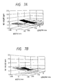
- Figs. 3A and 3B show states of bubbles remaining on the wafer.
- Fig. 3A illustrates positions and the number of dust particles not less than 0.2 ⁇ m on a 5-inch-diameter bulk wafer surface where only immersion was conducted but removal of bubbles was not carried out in the ultrasonic cleaning in pure water
- Fig. 3B similarly illustrates positions and the number of dust particles where removal of bubbles was carried out by lifting the wafer every five minutes.
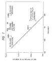
- the number of dust particles is 450 in Fig. 3A while it is 35 in Fig. 3B.
- the dust particles aggregate densely along the bubble rise direction (indicated by the arrow in each drawing) when the removal of bubble is not carried out, whereas the removal of bubble relieves this tendency.
- porous silicon having the hydrophobic surface is cleaned by this cleaning method for 20 minutes by superimposing the ultrasonic wave of 950 kHz on an ordinary-temperature over-flow pure water bath and lifting the substrate every five minutes out of the pure water bath for removal of bubble, approximately 30 % to 40 % of dust particles, which were unable to clean before, can be removed from the surface of porous substrate. With further repetition of the same cleaning for 20 minutes more, 60 % to 80 % of the dust particles before cleaning can be removed.
- the dust particles were removed by the cleaning method for cleaning the cleaned substrate with the pure water on which the ultrasonic wave in the high-frequency region is superimposed and for regularly lifting the cleaned substrate out of the pure water bath during cleaning.
- the method for regularly lifting the substrate out of the pure water bath during cleaning would be extremely cumbersome works, for example, if the cleaning should rely on labor of worker. Further, it is not easy to perfectly avoid generation of bubbles and adhesion thereof to the substrate during cleaning even by carrying out the bubble removing operation based on the regular lift, and a further improvement is desired in terms of reproducibility and stability of cleaning.
- Embodiment 2 was achieved as a result of further research, which is a method for cleaning the substrate with pure water from which dissolved gas is deaerated, thereby preventing contamination of the substrate due to the dust particles in the pure water, caused by generation of bubbles and adhesion thereof to the substrate during the ultrasonic cleaning.
- the present inventor also checked the number of bubbles generated by the ultrasonic waves of the frequencies of 47 kHz and 950 kHz with changing concentration of residual oxygen similarly and with also deaerating N 2 .
- the present inventor found that substantially no bubbles were generated around 6 ppm at 47 kHz or around 3 to 5 ppm at 950 kHz, so that deaeration (including N 2 ) was able to suppress the generation of bubble independently of the frequencies of ultrasonic wave so as to remove the dust particles from the substrate, thus achieving the present invention.
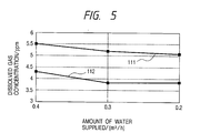
- the present inventor measured in great detail concentrations of dissolved gas in pure water in a square-shaped over-flow bath in a water supply state, using a dissolved oxygen/dissolved nitrogen sensor available from Orbisphere Laboratories, Inc. From the results of the measurement, when water was supplied from the bottom portion of the over-flow bath under irradiation of megasonic wave of power 600 W and frequency 950 kHz and, though depending upon the rate of water supplied as shown in Fig.
- the present inventors also used the pure water containing the dissolved oxygen in the concentration of 7.38 ppb and the dissolved nitrogen in the concentration of 14.57 ppm close to the saturation concentration thereof before, but bubbles were generated by megasonic irradiation if only the dissolved oxygen was deaerated and if the dissolved nitrogen existed 5 ppm or more.
- the bath used for cleaning is normally of such structure that the surface of liquid is open to the atmosphere and that even with the over-flow operation the gases composing the atmosphere (air) are re-dissolved into the liquid from the liquid surface and amounts thereof are not negligible.
- the pure water containing controlled concentrations of dissolved gases is always supplied by supplying deaerated water from the bath bottom portion and flows over to be drained out of the bath. This is considered to be a reason of capability of controlling the concentration of dissolved gas constant in the bath.
- Fig. 6A shows the concentration distribution of dissolved oxygen in the bath at the depth of 25 cm (at the bottom of bath)
- Fig. 6B shows the concentration distribution of dissolved oxygen in the bath at the depth of 12.5 cm (at the middle of the bath).
- Fig. 7A shows the concentration distribution of dissolved nitrogen in the bath at the depth of 12.5 cm
- Fig. 7B shows the concentration distribution of dissolved nitrogen in the bath at the depth of 25 cm.
- the arrow in the drawing indicates a direction of water supply in the bath bottom portion.
- the concentration of dissolved gas is lowest at the water supply port and the concentration increases with increasing distance from the water supply port along flow of the pure water in the bath bottom portion. At the depth 12.5 cm the concentrations were higher than in the bath bottom portion, but the concentration distributions were almost uniform, showing the oxygen concentration of about 150 ppb and the nitrogen concentration of about 1.8 ppm.
- turbulent flow occurs in the flow of water, depending upon the position and direction of the water supply port and the water supply rate, which increases the concentrations in the bath.
- concentrations in the bath are controlled by the concentrations of dissolved gases in the secondarily deaerated water, optimum design to keep the concentrations in the bath low as described above is necessary.
- concentrations of dissolved gases in the deaerated water in the over-flow bath under megasonic irradiation slightly increase with time of irradiation.
- Fig. 8A and Fig. 8B Concentration distributions of dissolved oxygen in the over-flow bath under megasonic irradiation of power 600 W and for 10 minutes from the bath bottom portion are shown in Fig. 8A and Fig. 8B and concentration distributions of dissolved nitrogen are shown in Fig. 9A and Fig. 9B.
- Fig. 8A shows the concentration distribution of dissolved oxygen at the depth of 25 cm (at the bath bottom) under megasonic irradiation
- Fig. 8B shows the concentration distribution of dissolved oxygen at the depth of 12.5 cm (at the middle of bath) under megasonic irradiation.
- Fig. 9A shows the concentration distribution of dissolved nitrogen at the depth of 25 cm under megasonic irradiation and Fig.
- the cleaning method of surface according to the present invention is arranged in such a way that cleaning for removing the dust particles adhering to the surface of substrate takes place with the pure water from which the dissolved gas is deaerated until the concentration of dissolved gas becomes 5 ppm or less and on which the ultrasonic wave is superimposed.
- the concentration of dissolved gas is 5 ppm or less means that the concentration of any dissolved gas, regardless of kinds of dissolved gases, is 5 ppm or less, but in general, it is sufficient that the concentrations of dissolved gases including oxygen, nitrogen, and CO 2 as the main components of air are 5 ppm or less.
- the small radius of cavitation and the high density thereof will result in excellent performance for removing particles of smaller particle sizes.
- the cavitation phenomenon splits water molecules by ultrasonic vibration, irrespective of the frequency, whereby a kind of small space in a vacuum state is made in the pure water. It is thus conceivable that this space expands and quickly contracts finally, thereby generating the sound pressure.
- the bubbles adhering to a hydrophobic substrate which are not removed by over flow, disappear several minutes (two to three minutes) after supply of the pure water deaerated to the limit with stopping the ultrasonic irradiation.
- Control of generation of bubble under ultrasonic irradiation by controlling the concentration of dissolved gas is nothing but decreasing the amount of gas remaining as bubbles by lowering the density of gas deaerated and discharged into the fine vacuum space.
- the above cleaning method of surface according to the present invention was found out in the process of experiments of the cleaning method of porous surface, but the fact that the bubbles are a cause of adhesion of dust particles is not specific to the porous surface.
- the invention can also be applied to cleaning of silicon wafer, SOI substrate, and so on, for example.
- the present invention is suitably applicable to cleaning of substrates having a hydrophobic surface, but it can also be applied to cleaning of substrates having a hydrophilic surface, wherein adhesion of dust particles can be prevented more certainly if generation of bubble is suppressed well.
- the cleaning method of porous surface according to the present invention is a method of cleaning for irradiating the surface of porous silicon substrate with the ultrasonic wave in the high-frequency band in the range of from 200 kHz to 8.4 MHz, preferably in the range of from 600 kHz to 2 MHz, more preferably in the range of from 800 kHz to 1.6 MHz, as superimposed on pure water, and using the pure water from which the dissolved gas is deaerated, thereby preventing contamination of substrate due to the dust particles in the pure water, caused by generation of bubble and adhesion thereof to the substrate during the ultrasonic cleaning, and thereby realizing short-time and stable cleaning of the porous silicon surface having the hydrophobic surface.
- the cleaning method of porous surface according to the present invention includes no specific limitation on the surface of substrate if the substrate has the surface of the porous structure.
- materials of substrate may be the semiconductor materials of Si, GaAs, or the like, the ceramic materials, and so on.
- the cleaning method of porous surface according to the present invention can also be used for removing the dust particles adhering to the substrate surface having the structure wherein a layer of semiconductor thin film of amorphous Si, polycrystal Si, GaAs, or the like or a layer of metal thin film is deposited by chemical vapor deposition or the like over the internal wall surfaces of pores of Si porous substrate, as shown in Fig. 2.
- Presently known methods for deaerating dissolved oxygen down to the dissolved oxygen concentration 5 ppb or less in the water, close to the limit concentration region, include film deaeration as a physical deaeration method and a method of combination of catalyst with a reducing method as a chemical deaeration method.
- the film deaeration method is popularly used in recent years, because it little contaminates the pure water and because it can remove the dissolved gases other than oxygen.
- the cleaning method of porous surface according to the present invention will be described further.
- Sources to generate bubbles are the gas captured in the inside after drying of porous silicon and discharged as replaced by the pure water out of the holes during the ultrasonic cleaning, and the dissolved gas such as oxygen and nitrogen dissolved in the pure water used for cleaning, which turn to bubbles because of the cavitation by ultrasonic.
- the bubbles adhering to the surface of hydrophobic substrate impede propagation of ultrasonic wave so as to lower the removing effect of dust particle, and in addition, they promote adsorption of dust particle to the substrate, thereby becoming the cause of contamination of the surface due to the dust particles and degradation of the cleaning effect.
- the bubbles adhering to the porous silicon surface can be removed by intermittently lifting the substrate out of the pure water during the ultrasonic cleaning.
- one of the causes of generation of bubble is the dissolved gas in the pure water used for cleaning, there will be naturally a limit of the cleaning effect even with such technique.
- an amount of bubbles deaerated from the inside of porous structure and fixed to the surface is considered to be far smaller than an amount of bubbles generated from the pure water.
- the bubbles themselves are not easy to deaerate in the case of the porous internal walls being hydrophobic, they are unlikely to be an element to impede the cleaning. Accordingly, when one of the causes to generate bubbles is the dissolved gas in the pure water used for cleaning, it is most effective to use the pure water from which the dissolved gas in the pure water is deaerated, as in the present invention, for further enhancing the cleaning effect of substrate.
- the gas dissolved in water is considered to be such that the concentration of dissolved oxygen in water is 8.26 ppm and the concentration of dissolved nitrogen is 13.9 ppm.
- the pure water used in the semiconductor fields is supplied under nitrogen purge of a pure water bath in a polishing system in order to maintain the purity of the pure water.
- the saturation dissolution concentration of nitrogen gas (purity: 99.999 %) under 25°C and 1 atm into the pure water becomes even 17.8 ppm.
- the dissolution concentration depends upon the temperature of water, and the concentration of nitrogen that can be dissolved decreases with increasing temperature of water.
- the present invention enabled only the high-frequency ultrasonic wave and the pure water from which the dissolved gas was removed, to remove the dust particles on the surface at high efficiency and in a short time with avoiding collapse of porous silicon.
- the action of the present embodiment is also effective to substrates other than silicon if they are substrates to be cleaned, having the fine and fragile porous structure similarly, and can demonstrate the same effect.
- the action and effect of the present invention are not limited to silicon.
- the porous silicon surface is subjected to the hydrophilic process and then to ultrasonic cleaning.
- the ultrasonic cleaning of porous silicon surface is carried out in the high frequency band of from 200 kHz to 8.4 MHz, preferably in the range of from 600 kHz to 2 MHz. More preferably, cleaning is carried out using the high-frequency ultrasonic wave in the frequency band as called megasonic cleaning ranging from 800 kHz to 1.6 MHz, thereby avoiding the risk of collapse of porous structure.
- the bubbles impede propagation of ultrasonic wave so as to degrade the cleaning effect and draw fine dust particles in the pure water to the gas-liquid interface so as to contaminate the substrate surface with the dust particles.
- Adhesion of bubbles to the substrate surface is little observed on the hydrophilic surface, whereas adhesion and fixing of bubble occurs on the hydrophobic surface. It is thus not easy to perfectly prevent adhesion of dust particles to the hydrophobic surface due to the bubbles, by the flowing water and ultrasonic wave in the cleaning bath.
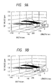
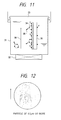
- Fig. 11 shows adhering states of bubbles and moving states of dust particles on the hydrophobic substrate, where the high-frequency wave is superimposed on the pure water.
- reference numeral 31 designates a quartz high-frequency cleaning bath, 32 a high-frequency vibrating plate, 33 pure water not subjected to deaeration of dissolved gas, 34 bubbles, 35 dust particles, 36 a porous silicon substrate having a hydrophobic surface, and 38 a high-frequency progressive wave.
- the low-frequency ultrasonic cleaning normally experiences generation of bubbles due to the cavitation in the pure water, whereas the high-frequency cleaning involves reduced cavitation, but experiences deaeration of dissolved gas due to high-frequency vibration in the pure water, thereby generating bubbles.
- the source of these bubbles is the dissolved gas such as oxygen and nitrogen dissolved in the pure water.
- the gas-liquid interface of bubble has higher energy than in the liquid and thus collects to capture fine dust particles in the pure water.
- the hydrophobic substrate surface is stable in terms of energy with respect to the gas, and the bubbles are thus likely to adhere thereto. Since the pure water cannot intrude into between the bubble and the substrate surface, it is difficult to remove the bubbles from the substrate. For example, while the bubbles are as small as about 1 mm in diameter, they cannot even move on the substrate surface only by buoyancy of themselves.
- the surface When the high-frequency ultrasonic wave is applied to the substrate surface, the surface receives kinetic energy in the direction of the progressive wave, but the energy is insufficient to move the bubbles, so that the bubbles are fixed to the substrate surface.
- Adhesion of the bubbles to the substrate surface promotes collection of fine dust particles in the pure water, and further adhesion of bubbles thereto causes the bubbles to move on the substrate surface by buoyancy of themselves, which makes the collected dust particles adhere to the substrate surface along the moving path thereof, thereby contaminating the substrate.
- the bubbles adhering to the substrate surface impede propagation of high-frequency wave to the substrate surface per se, thereby degrading the cleaning effect. Namely, generation of bubbles in the high-frequency cleaning of substrate having the hydrophobic surface will result in degrading the cleaning effect, because the high-frequency cleaning of dust particle on the substrate surface advances at the same time as the contamination of substrate by the dust particles in the pure water due to the adhesion of bubbles.
- the present inventor conducted the researches to improve the cleaning effect and found the method of Embodiment 1 for softly removing the bubbles by regularly lifting the substrate out of the pure water bath during cleaning and the method of Embodiment 2 for preliminarily deaerating the dissolved gas from the pure water used for cleaning so as to prevent the generation of bubble per se, thereby obviating the need for the lifting operation of substrate out of the pure water bath.
- Embodiment 3 for the porous silicon surface processed by the hydrophilic process.
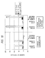
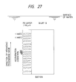
- Fig. 13 shows an example of flowchart of the fabrication process up to epitaxial growth on porous silicon and the cleaning method.
- SPM stands for H 2 SO 4 /H 2 O 2 mixture
- DIW for pure water
- DHF for dilute HF solution
- APM for NH 4 OH/H 2 O 2 /H 2 O mixture
- S/D spin drying.
- Cleaning of bulk silicon substrate before anodization is cleaning with chemicals, as before, but the apertures of holes of the porous structure are exposed in the substrate surface from after formation of porous silicon by anodization to epitaxial growth.
- the chemicals normally used for cleaning of bulk silicon substrate such as SPM, APM, or HPM (HCl/H 2 O 2 /H 2 O mixture) cannot be used while the apertures of holes of porous silicon are exposed in the surface. Only DHF and pure water can be used in that period.
- an oxide film is formed over the internal wall surfaces of porous structure (by forming a native oxide film or by a low-temperature oxidation step of Fig. 16) in order to decrease the structural change of the porous structure in the heating process at high temperatures.
- the epitaxial growth is carried out after at least the oxide film over the porous surface (of silicon substrate) is selectively removed immediately before the growth.
- the oxide film is left on the internal wall surfaces of holes of porous structure.
- the oxide film on the porous silicon surface is removed by immersion in DHF for a short time, the substrate is drawn up out of the DHF bath before the DHF solution deeply intrudes into the holes of porous structure, and the substrate is rinsed with pure water.
- an oxide film is formed by low-temperature oxidation of the internal walls of holes of porous silicon at 400°C and for one hour.
- the porous silicon surface becomes hydrophobic, as shown in Fig. 13, after the anodization, as after the removal of oxide film with DHF after the low-temperature oxidation.
- FIG. 12 shows the result of inspection where a state of adhesion of dust particles to the substrate surface was checked with a dust particle inspection system after the hydrophobic, porous silicon substrate was subjected to the high-frequency cleaning in pure water without performing the lift of substrate and the deaeration process of pure water.
- the arrow represents the rise direction of bubble.
- the high-frequency progressive wave is also applied so as to travel in the same direction. Adhesion contamination of dust particle is recognized along the rise path of bubbles adhering to the substrate surface.
- Deaeration of dissolved gas in the pure water can compensate for the gas concentrations at the exit of deaerating apparatus, but in the case of reserving water in a pure water high-frequency cleaning bath, redissolution of oxygen and nitrogen occurs from the atmosphere within a short time even under flow of water. Thus, some measure becomes necessary for the structure of cleaning bath, gas seal, and the like in order to compensate for the concentrations of dissolved gas in the pure water in the cleaning bath.
- the cleaning method of porous surface according to Embodiment 3 of the present invention is the method for oxidizing the porous surface into a hydrophilic surface so as to facilitate occurrence of the cleaning effect in the high-frequency cleaning with pure water and for removing the dust particles of substrate surface from the hydrophilic surface by the pure-water high-frequency cleaning.
- a single-crystal silicon film is epitaxially grown on the porous silicon surface after the etching removal with dilute HF solution, immediately before the epitaxially growth, of the clean surface oxide film of porous silicon substrate from which such dust particles have been removed, the single-crystal silicon film with good quality can be formed.
- the cleaning method of porous surface according to Embodiment 4 of the present invention is a method for oxidizing the porous surface into a hydrophilic surface so as to facilitate occurrence of the cleaning effect in the high-frequency cleaning and for superimposing the high-frequency ultrasonic wave on a liquid for cleaning of the porous surface made hydrophilic, thereby removing the dust particles on the substrate surface.
- the cleaning method of porous surface according to the present embodiment is not limited to specific materials of substrate if the substrate has the surface of the porous structure.
- applicable materials include the semiconductor materials of Si, GaAs, and the like, ceramic materials, and so on.
- the cleaning method of porous surface according to the present invention can also be applied for removing the dust particles adhering to the substrate surface having such structure that a film of semiconductor thin film of amorphous Si, polycrystal Si, GaAs, or the like or a layer of metal thin film is deposited by chemical vapor deposition or the like on the internal wall surfaces of pores of Si porous substrate, as shown in Fig. 2.
- the layer of the semiconductor thin film or the metal thin film may be formed directly on the internal wall surfaces of pores of the porous substrate as shown in Fig. 2, the layer of semiconductor thin film or metal thin film may be formed after the substrate surface oxide film and the internal wall oxide film formed by the hydrophilic process are removed.
- porous silicon immediately after anodization has the hydrophobic surface, because the conc HF mixture solution is used as an electrolyte solution.
- this surface becomes hydrophilic. If the surface is hydrophilic and even if bubbles are generated in high-frequency cleaning with non-deaerated pure water, the bubbles will not adhere to the substrate surface, whereby the high-frequency cleaning with pure water can demonstrate the cleaning effect with high removing rate.
- the substrate is made hydrophilic by low-temperature oxidation before the cleaning step S 12 as shown in Fig. 14, even with generation of bubbles on the hydrophilic substrate surface similarly, the substrate surface is stable and shows a good wetting property to pure water and, therefore, the substrate surface is always covered with pure water, thus preventing the bubbles from adhering thereto.
- the dust particles collected by the bubbles are prevented from transferring to the substrate and do not impede propagation of high-frequency wave, thus demonstrating the cleaning effect sufficiently.
- the pure-water high-frequency cleaning of hydrophilic substrate does not need to perform the countermeasure of the regular lift operation of substrate, the deaeration process of pure water, or the like, and the high cleaning action can be expected by keeping the substrate immersed in the pure-water high-frequency bath during cleaning even with generation of bubbles as in the case of the deaerated pure water.
- this low-temperature oxidation process is carried out as a process before epitaxial growth on porous silicon in order to decrease the structural change of the porous structure during the heating process at high temperatures, which is not one especially introduced for the cleaning of the present invention.
- the low-temperature-oxidized film is also formed by intrusion of oxide atom into the crystal lattice of substrate surface, similarly as in thermal oxidation, and if the dust particles are present on the surface it will be also formed at the interface between the particles and the substrate.
- the oxide film is removed from the surface by etching of oxide film together with the dust particles having adhered during the oxidation step.
- the dust particles will be brought into the etching bath unless the surface of oxide film before etching is clean. It will cause the dust particles to re-adhere to the substrate after etching.
- the cleaning after the oxidation step is carried out preferably before exfoliation of the oxide film by etching.
- porous silicon is made hydrophilic by oxidation or the like, thereafter it is subjected to the high-frequency cleaning with pure water to effectively remove the dust particles from the surface and to create a clean oxide film surface, exfoliation of the surface oxide film with the dilute HF solution is carried out immediately before epitaxial growth or the like, and then the epitaxial growth or the like is carried out, thus providing a clean porous silicon surface that can be used in the semiconductor processes.
- the dust particles on the oxide film surface which might be a cause of re-adhesion of dust particles in the dilute HF etching step, are already removed so as to secure the clean oxide film surface, whereby the dust particles are little brought into the dilute HF liquid bath, thus relieving the problem of re-contamination.
- the difference of the fabrication method of Fig. 14 from Fig. 13 is that the high-frequency cleaning with pure water carried out on the hydrophobic surface after the oxide film removing step of porous silicon surface with the dilute HF solution between the thermal oxidation step and the epitaxial growth step is changed to the pure-water high-frequency cleaning carried out on porous silicon having the hydrophilic surface between the oxidation step and the dilute HF etching step.
- the dust particles on the porous silicon surface can be removed effectively without a need for the countermeasure against adhesion of bubble, such as the regular substrate lift operation during cleaning or the deaeration of pure water.
- the hydrophilic process may be made using the oxidation action with ozone water or hydrogen peroxide water described hereinafter, instead of the thermal oxidation. In this case, though immersion of substrate is sufficient, it is more preferable to apply the high-frequency ultrasonic wave thereto.
- the hydrophilic process include dry oxidation processes, such as atmospheric pressure oxidation in a high-concentration ozone gas ambience or in a high-concentration oxidizing ambience, or a process by plasma oxidation under reduced pressure using the aforementioned gas as a base raw material.
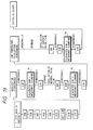
- step S 1 cleaning takes place in combination of the deaeration process of dissolved gas in the pure water with the high-frequency cleaning with pure water of hydrophobic surface.
- Such a cleaning step including the deaeration process can be replaced by the cleaning method of the present invention as shown in Fig. 15.
- the step S 11 of Fig. 15 is according to the cleaning method of porous surface based on the second embodiment of the present invention, wherein high-frequency cleaning takes place with pure water in which ozone is dissolved.
- the pure water with ozone dissolved therein has strong oxidizing action.
- the removing effect of organic matter greatly depends upon the oxidizing action of organic matter.
- the strong oxidizing action of the ozone pure water can be used as the hydrophilic process of hydrophobic surface, and has an effect to create the hydrophilic surface by oxidizing the porous silicon surface after anodization. If the hydrophilic surface thus created is subjected to the high-frequency cleaning, the hydrophilic process and high-frequency cleaning will be performed in one step.
- the ozone pure water intrudes into the pores of porous silicon like the pure water, it can be eliminated readily as vapor or oxygen gas by heating after the process, thus leaving no negative effect on the subsequent steps.
- the oxide film over the porous silicon surface and over the internal walls of holes made by the ozone water containing ozone in the concentration of about 10 to 13 % is removed by etching with DHF, which was carried out conventionally for the purpose of removing the native oxide film prior to the low-temperature oxidation step.
- the high-frequency cleaning with the ozone pure water demonstrates the effect on the hydrophobic porous silicon surface, but no problem will arise if it is applied to cleaning of oxidized porous silicon already having the hydrophilic surface. Accordingly, the cleaning method can be used for cleaning of porous silicon both after anodization and after low-temperature oxidation.
- Fig. 15 may be modified as shown in Fig. 16 wherein low-temperature oxidation takes place after the high-frequency cleaning with pure water in which ozone is dissolved.
- An oxide film is formed by the ozone pure water on the porous silicon surface after anodization, and the low-temperature thermal oxidation process achieves uniform oxidation proceeding deeply into the holes of the porous inner walls.
- the oxide film exfoliation step before the low-temperature thermal oxidation becomes unnecessary, thus further decreasing the steps as shown in Fig. 16.
- hydrophobic substrate becomes hydrophilic after APM cleaning, but APM cannot be used for the hydrophilic process of hydrophobic porous silicon as described previously.
- a semiconductor substrate made clean in a manner of the present invention as explained above which substrate has a porous surface may be suitably used for a preparation of a semiconductor device such as MOS-FET.
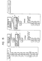
- Fig. 29A through 29F are cross-sectional views to schematically show an example of processes of such a semiconductor device.
- silicon substrate 40 which has been made clean in the above-explained manner, is comprised of non-porous silicon single crystal region 42 (i.e. bulky silicon region) remaining without being made to be porous and porous silicon single crystal layer 41.
- silicon substrate 40 was heated at 400°C for 1 hour in oxygen atmosphere, whereby oxide films were formed on inner walls of pores of porous silicon single crystal layer 41 and a surface of porous silicon single crystal layer 41, respectively. It is for preventing silicon atoms from a migration in the pore as the result of the raising of temperature in a process of forming an epitaxial layer at a later stage and so forth and the pores from filling up as the result of the migration that the films were provided.
- non-porous silicon single crystal layer (epitaxial layer) 43 of 0.3 ⁇ m in thickness was made to grow epitaxially on porous Fig.29B.
- Any of molecular beam epitaxial method, plasma CVD method, reduced pressure CVD method, light CVD method, liquid-phase growth method and sputtering method can be used for forming such non-porous silicon single crystal layers as layer 43.
- the layer is typically formed in a range of 100 nm through 2 ⁇ m in thickness.
- the surface of non-porous silicon single crystal layer 43 was partially oxidised, to form oxide film of 200 nm in thickness, as insulating layer 44.
- oxide film of 200 nm in thickness
- the layer is typically formed in a range of 50 nm through 2 ⁇ m in thickness.
- Fig. 29D another silicon substrate 45 was laid on top of insulating layer 44 and then the laid faces of them were stuck on each other.
- the resultant was heat treated at 1180°C for 5 minutes to adhere the faces to each other.
- silicon substrate 40 as the first substrate and silicon substrate 45 as the second substrate were adhered to each other through insulating layer 44, so that multilayer structure 50 wherein non-porous silicon single crystal layer 43 was located was formed as shown in Fig. 29D.
- non-porous silicon single crystal region 42 was removed from the above-mentioned multi-layer structure 50, to expose porous silicon single crystal layer 41 in a manner as described in the following: First, non-porous silicon single crystal layer 42 was ground by a grinder so as to leave the layer 42 in a slight thickness from the border with porous silicon single crystal layer 41, followed by removing the remaining non-porous silicon single crystal region 42 from by means of dry-etching. Besides such a grinding method, it is able to employ a method of separating non-porous silicon single crystal region 42 from multi-layer structure 50 on the basis of porous silicon single crystal layer 41 as the border.
- porous silicon crystal layer 41 Since the mechanical strength of porous silicon crystal layer 41 is lesser than that of non-porous silicon single crystal region 42, non-porous silicon single crystal layer 43 and so forth, it is possible to separate non-porous silicon single crystal region 42 without causing damage to non-porous silicon single crystal layer 43, by giving between silicon substrate 45 and non-porous silicon single crystal region 42 a force of pulling apart in a direction perpendicular to the surface of the substrate or a shear force in a direction parallel to the surface of the substrate.
- methods of inserting a wedge-shaped member or blowing water jet to porous silicon single crystal layer 41 are exemplified.
- non-porous silicon single crystal region 42 is capable of baring porous silicon single crystal layer 41 in a short time, so that the semiconductor device can be manufactured efficiently.
- non-porous silicon single crystal region 42 a portion of porous silicon single crystal layer 41 which remains after the separation and than flattening the region as occasion demands, followed by making it porous partially, to utilise non-porous silicon single crystal region 42 as such silicon substrate 40 as shown in Fig.29A.
- porous silicon single crystal layer 41 was removed by etching, to form on silicon substrate 45 so-called SOI (silicon-on-insulator) substrate 51, which has thin non-porous silicon single crystal layer 43 through insulating layer 44.
- SOI silicon-on-insulator
- a chemical etching method where an aqueous solution containing hydrofluoric acid and hydrogen peroxide water is used as an etchant was employed for the etching of porous silicon single crystal layer 41.
- the etching rate by such an etchant on porous silicon is 1x10 5 times greater than that on non-porous silicon. Accordingly, it was able to remove selectively and controllably porous silicon single crystal layer 41, leaving flat non-porous silicon single crystal layer 43 which is uniform in thickness.
- SOI substrate 51 shown in Fig. 29F was heat treated at 1100°C for lhr in hydrogen atmosphere, to further flatten the surface of non-porous silicon crystal layer 43.
- Mean square roughness of the surface after this heat treatment measured by interatomic force microscope was about 0.2 nm.
- non-porous silicon single crystal layer 43 of SOI substrate 51 formed in such a manner as described above it is capable of manufacturing a semiconductor device such as MOS-FET, DRAM, solar cell and so forth through a well-known semiconductor process.
- the product in the above-mentioned example, it was a silicon substrate that was used as the second substrate.
- a photo-transmittable substrate such as quartz substrate and glass substrate can be used.
- the product can be suitably used for photo-sensor, liquid crystal display and so forth.
- the second substrate is comprised of an insulating material such as quartz substrate and glass substrate, or when using as the second substrate a silicon substrate wherein an insulating layer such as Si0 2 layer was formed on the adhered face, insulating layer 44 in Fig. 29C is not indispensable.
- non-porous silicon single crystal layer 43 on which a semiconductor device is to be formed in a future process, should be separated from the adhered face as far as possible to protect it from an influence of an impurity and so forth, it is desirable to form an insulating layer on non-porous silicon single crystal layer 43.
- the pure water used was obtained by treating and filtering service water to satisfy the following conditions of purity.
- Porous silicon substrates used in cleaning were prepared by forming a porous silicon layer 10 ⁇ m thick on one side of p + -the 5-inch-diameter silicon substrate RCA-cleaned, by anodization,and then they were subjected to pure-water rinse and spin drying. Then the number of dust particles was measured for each sample using a surface dust particle inspection system.
- the above porous silicon substrates 3 were set in the order of anodization batches on a cleaning carrier 4 in a Fig. 17. Then they were cleaned as applying the high-frequency ultrasonic wave of the frequency of about 1MHz and the power of 150 W in parallel with the substrates 3 from an oscillator 6 of high-frequency ultrasonic bath 5 through the quartz bath 2.
- a bulk silicon substrate 7 RCA-cleaned was placed as a dummy for cleaning at the carrier end, and the substrates were cleaned in the pure water for 20 minutes as eliminating the bubbles adhering thereto by lifting the substrates together with the carrier 4 out of the pure water every five minutes.
- the substrates were subjected to spin drying after cleaning and then measurement of dust particles was carried out. The same cleaning was again conducted for 20 minutes more and then measurement of dust particles was conducted.
- the measurement of dust particles was evaluated in the mode to measure dust particles of sizes not less than 0.3 ⁇ m, attained from the laser reflection intensity distribution in the 5-inch substrate surface.
- Fig. 18 shows changes in the number of dust particles with this series of cleanings. In this figure values of % indicate removal rates. Fig. 18 does not include data of the dummy 7 at the carrier end.
- Porous silicon conventionally used was the one cleaned only by pure water rinse and thus having the surface contaminated with dust particles.
- the substrates were set on the carrier in the same method as described above and were immersed in diluted hydrofluoric acid. Then the pure-water over-flow high-frequency ultrasonic cleaning was carried out in the cleaning system (Fig. 17) of Example 1 for 20 minutes as eliminating the adhering bubbles by lifting the substrates together with the carrier 4 every five minutes (F in the drawing). As shown in Fig. 18, 54 % to 80 % of dust particles were removed as compared with the data immediately after oxidation and the number of dust particles was not more than 65 in either one of the porous silicon substrates.
- Example 1 Now described is the removing effect of adhering bubbles in the high-frequency cleaning in pure water carried out in Example 1 and Example 2.
- Adsorption by bubbles is outstanding with fine dust particles and the collectively adhering state thereof to the substrate surface is outstanding.
- generation of bubbles from dissolved gas in pure water is observed even in the high-frequency band as described previously.
- bubbles are supposed to be generated because the gas (air) in the pores thereof are replaced with pure water to be discharged out of the pores.
- evaluation thereof was conducted by the dust particles not less than 0.2 ⁇ m on a hydrophobic bulk substrate surface without any porous structure formed therein.
- Fig. 19 is a drawing to show the result of measurement of the number of dust particles conducted in such a way that bulk substrates were preliminarily cleaned by RCA cleaning to minimize the number of dust particles on the surface, they were immersed in diluted hydrofluoric acid, thereafter they were rinsed with pure water for 5 minutes, they were dried by spin drying, and then the number of dust particles was measured. It is apparent that the number of dust particles on the substrate at the carrier end is larger than those on the substrates at the other positions. This is considered to be due to inductive charging of the closest wafer induced by carrier charge, as well known. Numbers indicating slot positions in the drawing represent slot numbers of the wafer carrier frequently used heretofore in the semiconductor industrial fields, and slots are formed at equal intervals of the pitch of 5 mm from 1 to 25 from the carrier end.
- Fig. 20 is a drawing to show numbers of dust particles where the high-frequency cleaning of the frequency 1 MHz and the power 150 W was carried out in the above five-minute pure-water rinse step. As shown in Fig. 20, the high-frequency cleaning decreases the number of dust particles on the substrate, but, depending upon the slot position of wafer carrier, some substrates show an extreme increase of fine dust particles (L1) on the contrary.
- Fig. 21 is a drawing to show numbers of dust particles where only the dust particle measuring surface of the substrate at the carrier end was reversely set with respect to the carrier side, the other wafers in the carrier were normally set, and removal of bubbles was conducted by repeating the operation of lifting the substrates together with the carrier out of the high-frequency pure water bath every five minutes and again immersing them into the pure water, for 20 minutes.
- the cleaning effect can be enhanced further by repeating the lift operation of substrate every short time within the same cleaning period so as to further decrease the number of adhering bubbles in the cleaning period of time in pure water.
- Fig. 22 shows the numbers of dust particles after cleaning in the normal state
- Fig. 23 shows the numbers of dust particles after cleaning which was conducted with the bulk substrate being set in the reverse state in the slot at the carrier end where the influence of inductive charging was greater from the carrier.
- the number of particles on the substrate at the carrier end is prominent as in the case of immersion in diluted hydrofluoric acid, but in the case of the reverse setting, the number is so small as to show little difference when compared with those of the other substrates.
- the conditions including the frequency and high-frequency power, the cleaning period of time, the temperature of liquid, etc. are just an example for verifying the cleaning effect of the present invention, and the present invention is limited only by the frequency band (from 600 kHz to 2 MHz), but the other conditions can be set arbitrarily.
- the examples of the present invention described examples where the high-frequency wave was superimposed on pure water, but, from the fact that the removing effect of organic matter and dust particles is well known where a small amount of surfactant, ozone, or the like is added to the pure water, methods in combination of these with the high-frequency cleaning of porous silicon surface specific to the present invention can be readily achieved from the present invention.
- the above examples showed the examples of silicon semiconductor as a substrate material having the porous structure, but it is apparent in the above description that the object of the present invention is to clean the substrate having the fine, dense, fragile, porous structure in its cleaned surface.
- the cleaning method of the present invention can be applied to any substrates having the similar porous structure, and the invention is not limited by the substrate material.
- Examples 3 and 4 are examples of Embodiment 2.
- a film deaeration apparatus 11 in Example 3 is used as connected midway of a pure water supply pipe between the conventional pure water producing apparatus 12 and the ultrasonic cleaning apparatus 13.
- the pure water produced by the film deaeration apparatus 11 is desirably released from the bottom part of the ultrasonic cleaning apparatus 13 in order to avoid take-in of air.
- Porous silicon substrates each having a hydrophobic surface obtained by removing the surface native oxide film were set on the cleaning carrier in a quartz bath under over flow of flowing water, using deaerated pure water, and the ultrasonic cleaning (the frequency 950 kHz) was conducted as applying the high-frequency ultrasonic wave of power 150 W in parallel to the substrate from the oscillator of the high-frequency ultrasonic bath through the quartz bath during immersion for 20 minutes. The cleaning was carried out only by immersion without performing the lift operation of substrate.
- Fig. 27 schematically shows the relationship between the porous silicon substrate and the high-frequency progressive wave. The removing effect of dust particles adhering to the porous silicon substrate can be enhanced by placing the cleaned surface of porous silicon substrate in parallel with the travel direction of the high-frequency progressive wave as shown.
- Fig. 25 shows comparison of dust particle removal rates of porous surface among the case of the conventional high-frequency cleaning (case B) where cleaning was continued for 20 minutes under the same ultrasonic conditions by using non-deaerated pure water and performing the substrate lift operation every five minutes, the conventional case (case C) where the same cleaning was further continued for 20 minutes more (for 40 minutes in total), and the case (case A) where cleaning was conducted under the above cleaning conditions of the present invention for only immersion in deaerated pure water.
- the cleaning effect of the present invention is by no means limited to the immersion cleaning of substrate in the pure water bath like above Example 3.
- Examples 5 to 8 are examples of Embodiment 3.
- the cleaning flow of Example 5 up to the epitaxial growth of porous silicon substrate is the same as the cleaning flow shown in Fig. 13.
- the cleaning steps S 2 , S 3 are omitted in this example.
- the cleaning steps S 2 , S 3 can be performed with necessity, of course.
- Cleaning was conducted to process one dummy substrate at the end of polytetrafluoroethylene (Teflon) carrier for cleaning and twenty four porous silicon substrates together and was continued for 20 minutes under the conditions of the frequency of 950 kHz, the high-frequency power 150 W, the ordinary temperature, and over flow of flowing water with the substrates being kept immersed.
- Teflon polytetrafluoroethylene
- step S 1 The pure water was one deaerated before the concentration of dissolved gas became 5 ppb or less. This cleaning removed almost 90 % of dust particles which have adhered in the anodization step.
- the porous silicon surface thus cleaned is hydrophobic, but a native oxide film is formed thereon during the period of storage. Accordingly, immediately before the low-temperature oxidation process, the high-frequency cleaning with pure water and the exfoliation of the native oxide film with DHF were conducted again, and a thermal oxide film was formed in dry oxygen, at the low temperature of 400°C, and for one hour.
- the surface after the low-temperature oxidation becomes hydrophilic, but approximately 100 dust particles newly adhere to the substrate surface during the oxidation step. Therefore, the high-frequency cleaning with pure water was carried out after the oxidation to remove the dust particles on the surface and to create a clean oxide film surface, and the substrates were stored in a dedicated box.
- the countermeasure to prevent the bubbles from adhering to the substrate surface is unnecessary and the substrates can be cleaned as immersed in the high-frequency cleaning bath with non-deaerated pure water.
- the substrates were cleaned for 20 minutes under the cleaning conditions of the frequency of 950 kHz, the high-frequency power 150 W, the ordinary temperature, and immersion in the flowing water over-flow bath, using the non-deaerated pure water and keeping the substrates immersed.
- This cleaning removed 90 % of dust particles which have adhered in the oxidation step. Storage after oxidation and cleaning, even if long, raises no problem at all in applications of porous silicon, because it is covered by the oxide film.
- porous silicon substrates with the oxide film, having been stored, of the number that could be processed by the epitaxial growth system were subjected to exfoliation removal of only the oxide film on the porous silicon surface with DHF immediately before introduced into the epitaxial growth system, and then epitaxial growth was conducted.
- the epitaxial growth made a film with the surface of porous silicon as the origin, and therefore, the oxide film over the internal walls of holes of porous silicon were left in the etching step with DHF.
- deaerated pure water Two types of pure water used in the above high-frequency cleaning with pure water, deaerated and non-deaerated, were used depending upon the surface state of substrate, but the deaerated pure water may be used for both the hydrophobic surface (after anodization) and the hydrophilic surface (after low-temperature oxidation) or the lift operation of substrate (without deaeration) may be carried out.
- Fig. 15 shows the cleaning flow of the present example.
- the high-frequency cleaning with deaerated pure water was carried out to clean the hydrophobic porous silicon surface after anodization in above Example 1, whereas in the present example the high-frequency cleaning was carried out under the same conditions using ozone pure water in which ozone dissolved in approximately 10 to 13 %.
- the ozone pure water used herein was the one obtained by dissolving ozone gas, obtained from a wet type ozone producing system in combination of a hollow fiber filter with electrolysis of pure water as well known, in pure water.
- the oxide film formed over the surface of porous silicon and the internal walls of holes by the ozone pure water after anodization is removed by etching with DHF immediately before the low-temperature oxidation step, similar to that heretofore.
- step S 12 of Fig. 15 can be performed under the same conditions as in step S 11 ).
- the cleaning flow is the same as in Example 6, but it was modified, though not illustrated, to a method of high-frequency cleaning after the hydrophobic porous silicon surface after anodization was made hydrophilic with hydrogen peroxide solution (H 2 O 2 /H 2 O) of a low concentration of approximately 2 % or less diluted with pure water, instead of the high-frequency cleaning carried out after the hydrophobic porous silicon surface after anodization has been changed to the hydrophilic surface with the ozone pure water.
- hydrogen peroxide solution H 2 O 2 /H 2 O
- the cleaning method demonstrated the cleaning effect even with keeping the substrate immersed, similarly as in use of the deaerated pure water or the ozone pure water.
- the pure water used in cleaning in the present example was subject to over flow of flowing water, the dust particles removed were discharged with water out of the cleaning bath, the diluted hydrogen peroxide solution thus discharged was guided through a filter for capturing particles of about 0.1 ⁇ m, then the hydrogen peroxide solution was recirculated to the cleaning bath, and the high-frequency cleaning was conducted as thus supplying the hydrogen peroxide solution. A certain amount of hydrogen peroxide was regularly replenished to compensate for consumption thereof.
- cleaning in the cleaning bath is suitable for totally processing many substrates, but the recent demand for further increase of size of substrate will increase the volume of the cleaning bath, i.e., increase the chemicals used.
- a method for solving this problem is a combination of the high-frequency cleaning with pure water according to the present invention with a single wafer type cleaning apparatus in combination of the well-known chemical shower with exhaust of chemicals by spinner.
- the present invention is basically cleaning with pure water, and has an advantage that cleaning can be made cheaper than in use of chemicals.
- the single wafer type shower cleaning is suitable for cleaning of porous silicon surface after anodization because of its process performance.
- the surface is made hydrophilic by oxidation before cleaning or by a shower of ozone water or diluted hydrogen peroxide solution and then the high-frequency cleaning is conducted, thereby effectively removing the dust particles adhering thereto.
- the high-frequency cleaning using the pure water shower can also be applied to cleaning of the porous silicon surface having the hydrophilic surface made by the low-temperature oxidation.
Landscapes
- Engineering & Computer Science (AREA)
- Physics & Mathematics (AREA)
- Condensed Matter Physics & Semiconductors (AREA)
- General Physics & Mathematics (AREA)
- Manufacturing & Machinery (AREA)
- Computer Hardware Design (AREA)
- Microelectronics & Electronic Packaging (AREA)
- Power Engineering (AREA)
- Cleaning Or Drying Semiconductors (AREA)
Applications Claiming Priority (9)
| Application Number | Priority Date | Filing Date | Title |
|---|---|---|---|
| JP15763296 | 1996-05-28 | ||
| JP15763296 | 1996-05-28 | ||
| JP157632/96 | 1996-05-28 | ||
| JP14283796 | 1996-06-05 | ||
| JP142837/96 | 1996-06-05 | ||
| JP142836/96 | 1996-06-05 | ||
| JP14283796 | 1996-06-05 | ||
| JP14283696 | 1996-06-05 | ||
| JP14283696 | 1996-06-05 |
Publications (3)
| Publication Number | Publication Date |
|---|---|
| EP0810643A2 true EP0810643A2 (fr) | 1997-12-03 |
| EP0810643A3 EP0810643A3 (fr) | 1998-03-11 |
| EP0810643B1 EP0810643B1 (fr) | 2005-08-31 |
Family
ID=27318518
Family Applications (1)
| Application Number | Title | Priority Date | Filing Date |
|---|---|---|---|
| EP97303616A Expired - Lifetime EP0810643B1 (fr) | 1996-05-28 | 1997-05-28 | Méthode de nettoyage d'une surface poreuse d'un substrat semiconducteur |
Country Status (7)
| Country | Link |
|---|---|
| EP (1) | EP0810643B1 (fr) |
| KR (1) | KR100370312B1 (fr) |
| CN (1) | CN1132229C (fr) |
| CA (1) | CA2206139C (fr) |
| DE (1) | DE69734078T2 (fr) |
| SG (1) | SG66370A1 (fr) |
| TW (1) | TW355815B (fr) |
Cited By (10)
| Publication number | Priority date | Publication date | Assignee | Title |
|---|---|---|---|---|
| EP0936663A2 (fr) * | 1998-01-14 | 1999-08-18 | Canon Kabushiki Kaisha | Méthode d'enlèvement d'une région poreuse et méthode de fabrication d'un substrat semiconducteur |
| US6001189A (en) * | 1996-09-30 | 1999-12-14 | Micron Technology, Inc. | Method for reducing gaseous species of contamination in wet processes |
| EP1000673A2 (fr) * | 1998-11-10 | 2000-05-17 | International Business Machines Corporation | Système pour nettoyer des plaquettes semiconductrices avec une onde mégasonique progressive |
| EP1039517A2 (fr) * | 1999-03-26 | 2000-09-27 | Canon Kabushiki Kaisha | Procédé de nettoyage d'un corps poreux et procédé de fabrication d'un corps poreux, d'un film non poreux ou d'un substrat soudé |
| DE19855895C2 (de) * | 1997-12-29 | 2002-09-19 | Mitsubishi Electric Corp | Reinigungsverfahren unter Verwendung einer Chlorwasserstoffsäure/Wasserstoffperoxid-Mischung |
| US6943115B2 (en) | 2000-06-23 | 2005-09-13 | Fujitsu Limited | Semiconductor device and method of manufacture thereof |
| EP2226834A3 (fr) * | 2009-03-06 | 2011-11-30 | Imec | Procédé pour nettoyage assisté par force physique avec des dommages réduits |
| CN110624893A (zh) * | 2019-09-25 | 2019-12-31 | 上海华力集成电路制造有限公司 | 一种兆声波组合气体喷雾清洗装置及其应用 |
| CN112452918A (zh) * | 2020-10-30 | 2021-03-09 | 怀化市盛德生物科技有限责任公司 | 一种农业产品进料清洗清洁机构 |
| CN113289972A (zh) * | 2021-04-27 | 2021-08-24 | 华能阜新风力发电有限责任公司 | 一种适用于散热片的节能清洁装置 |
Families Citing this family (15)
| Publication number | Priority date | Publication date | Assignee | Title |
|---|---|---|---|---|
| US6391067B2 (en) | 1997-02-04 | 2002-05-21 | Canon Kabushiki Kaisha | Wafer processing apparatus and method, wafer convey robot, semiconductor substrate fabrication method, and semiconductor fabrication apparatus |
| JPH10223585A (ja) | 1997-02-04 | 1998-08-21 | Canon Inc | ウェハ処理装置及びその方法並びにsoiウェハの製造方法 |
| CN1071713C (zh) * | 1998-11-11 | 2001-09-26 | 华南师范大学华南量子电子学研究所 | 砷化镓、磷化镓衬底干处理方法 |
| JP2013157443A (ja) * | 2012-01-30 | 2013-08-15 | Siltronic Ag | 洗浄方法 |
| JP5872382B2 (ja) * | 2012-05-24 | 2016-03-01 | ジルトロニック アクチエンゲゼルシャフトSiltronic AG | 超音波洗浄方法 |
| CN103736690B (zh) * | 2013-12-31 | 2018-12-18 | 上海集成电路研发中心有限公司 | 硅片清洗方法 |
| CN105618423A (zh) * | 2014-10-15 | 2016-06-01 | 北京华兴太极信息科技有限责任公司 | 多层印制板去除孔壁钻污生产线用超声震动清洗处理方法 |
| JP6658354B2 (ja) | 2016-06-30 | 2020-03-04 | 株式会社Sumco | 試料表面の作製方法、試料表面の分析方法、電界支援酸化用プローブおよびこれを備えた走査型プローブ顕微鏡 |
| CN106925565B (zh) * | 2017-02-09 | 2018-08-24 | 同济大学 | 一种lbo晶体的刻蚀清洗方法 |
| SG11202007002YA (en) * | 2018-01-23 | 2020-08-28 | Acm Res Shanghai Inc | Methods and apparatus for cleaning substrates |
| WO2019153134A1 (fr) * | 2018-02-07 | 2019-08-15 | Acm Research (Shanghai) Inc. | Procédé et appareil de nettoyage de substrats |
| CN111085497A (zh) * | 2019-12-18 | 2020-05-01 | 武汉百臻半导体科技有限公司 | 一种多晶硅片清洗系统及其清洗方法 |
| CN111659640B (zh) * | 2020-05-14 | 2022-03-18 | 富乐德科技发展(大连)有限公司 | 半导体设备腔体内铝基材多孔分气装置超洁净清洗工艺 |
| CN112921326B (zh) * | 2021-01-22 | 2022-11-08 | 广东威圳兴技术有限公司 | 一种汽车零件压铸铝合金表面处理工艺 |
| CN118491956B (zh) * | 2024-07-17 | 2024-09-10 | 山东省农业技术推广中心(山东省农业农村发展研究中心) | 一种食用菌菌渣再利用清洗设备及其清洗方法 |
Citations (9)
| Publication number | Priority date | Publication date | Assignee | Title |
|---|---|---|---|---|
| JPS62198127A (ja) * | 1986-02-25 | 1987-09-01 | Sanyo Electric Co Ltd | 半導体ウエハの洗浄方法 |
| JPH0314230A (ja) * | 1989-06-13 | 1991-01-22 | Toshiba Corp | 半導体ウェーハの洗浄方法及び装置 |
| JPH04144131A (ja) * | 1990-10-05 | 1992-05-18 | Toshiba Corp | 半導体ウェーハの処理方法 |
| JPH04165620A (ja) * | 1990-10-30 | 1992-06-11 | Sony Corp | ウエハの洗浄方法 |
| EP0502237A1 (fr) * | 1991-02-28 | 1992-09-09 | Seiji Kagawa | Appareil pour fabrication de films poreux |
| EP0572211A1 (fr) * | 1992-05-25 | 1993-12-01 | Yoshihide Shibano | Méthode de nettoyage ultra-sonique d'une pièce |
| JPH06168660A (ja) * | 1992-11-30 | 1994-06-14 | Sony Corp | 含浸形カソード及びその製造方法 |
| JPH06254521A (ja) * | 1993-03-08 | 1994-09-13 | Olympus Optical Co Ltd | 脱脂洗浄方法 |
| US5427977A (en) * | 1992-04-30 | 1995-06-27 | Fujitsu Limited | Method for manufacturing porous semiconductor light emitting device |
Family Cites Families (1)
| Publication number | Priority date | Publication date | Assignee | Title |
|---|---|---|---|---|
| JPH06275866A (ja) * | 1993-03-19 | 1994-09-30 | Fujitsu Ltd | ポーラス半導体発光装置と製造方法 |
-
1997
- 1997-05-23 TW TW086106988A patent/TW355815B/zh active
- 1997-05-26 CA CA002206139A patent/CA2206139C/fr not_active Expired - Fee Related
- 1997-05-28 DE DE69734078T patent/DE69734078T2/de not_active Expired - Lifetime
- 1997-05-28 CN CN97105404A patent/CN1132229C/zh not_active Expired - Fee Related
- 1997-05-28 EP EP97303616A patent/EP0810643B1/fr not_active Expired - Lifetime
- 1997-05-28 KR KR1019970021273A patent/KR100370312B1/ko not_active IP Right Cessation
- 1997-05-28 SG SG1997001766A patent/SG66370A1/en unknown
Patent Citations (9)
| Publication number | Priority date | Publication date | Assignee | Title |
|---|---|---|---|---|
| JPS62198127A (ja) * | 1986-02-25 | 1987-09-01 | Sanyo Electric Co Ltd | 半導体ウエハの洗浄方法 |
| JPH0314230A (ja) * | 1989-06-13 | 1991-01-22 | Toshiba Corp | 半導体ウェーハの洗浄方法及び装置 |
| JPH04144131A (ja) * | 1990-10-05 | 1992-05-18 | Toshiba Corp | 半導体ウェーハの処理方法 |
| JPH04165620A (ja) * | 1990-10-30 | 1992-06-11 | Sony Corp | ウエハの洗浄方法 |
| EP0502237A1 (fr) * | 1991-02-28 | 1992-09-09 | Seiji Kagawa | Appareil pour fabrication de films poreux |
| US5427977A (en) * | 1992-04-30 | 1995-06-27 | Fujitsu Limited | Method for manufacturing porous semiconductor light emitting device |
| EP0572211A1 (fr) * | 1992-05-25 | 1993-12-01 | Yoshihide Shibano | Méthode de nettoyage ultra-sonique d'une pièce |
| JPH06168660A (ja) * | 1992-11-30 | 1994-06-14 | Sony Corp | 含浸形カソード及びその製造方法 |
| JPH06254521A (ja) * | 1993-03-08 | 1994-09-13 | Olympus Optical Co Ltd | 脱脂洗浄方法 |
Non-Patent Citations (8)
| Title |
|---|
| O.I. BABIKOV: "Ultrasonic modular units for cleaning semiconductor structures in deionized water with increased intensity of the piezoceramic transducers" ELEKTROTEKHNIKA, vol. 62, no. 6, 1991, pages 74-77, XP002050135 * |
| PATENT ABSTRACTS OF JAPAN vol. 012, no. 049 (E-582), 13 February 1988 & JP 62 198127 A (SANYO ELECTRIC CO LTD;OTHERS: 01), 1 September 1987, * |
| PATENT ABSTRACTS OF JAPAN vol. 016, no. 420 (E-1259), 4 September 1992 & JP 04 144131 A (TOSHIBA CORP), 18 May 1992, * |
| PATENT ABSTRACTS OF JAPAN vol. 018, no. 493 (E-1606), 14 September 1994 -& JP 06 168660 A (SONY CORP), 14 June 1994, * |
| PATENT ABSTRACTS OF JAPAN vol. 018, no. 651 (C-1285), 9 December 1994 -& JP 06 254521 A (OLYMPUS OPTICAL CO LTD), 13 September 1994, * |
| PATENT ABSTRACTS OF JAPAN vol. 15, no. 130 (E-1051), 29 March 1991 -& JP 03 014230 A (TOSHIBA CORP.), 22 January 1991, * |
| PATENT ABSTRACTS OF JAPAN vol. 16, no. 465 (E-1270), 28 September 1992 & JP 04 165620 A (SONY CORP.), 11 June 1992, * |
| YONEHARA T ET AL: "EPITAXIAL LAYER TRANSFER BY BOND AND ETCH BACK OF POROUS SI" APPLIED PHYSICS LETTERS, vol. 64, no. 16, 18 April 1994, pages 2108-2110, XP000440703 * |
Cited By (18)
| Publication number | Priority date | Publication date | Assignee | Title |
|---|---|---|---|---|
| US6521049B1 (en) | 1996-09-30 | 2003-02-18 | Micron Technology, Inc. | Method for reducing gaseous species of contamination in wet processes |
| US6001189A (en) * | 1996-09-30 | 1999-12-14 | Micron Technology, Inc. | Method for reducing gaseous species of contamination in wet processes |
| US6866049B2 (en) | 1996-09-30 | 2005-03-15 | Micron Technology, Inc. | Device addressing gas contamination in a wet process |
| DE19855895C2 (de) * | 1997-12-29 | 2002-09-19 | Mitsubishi Electric Corp | Reinigungsverfahren unter Verwendung einer Chlorwasserstoffsäure/Wasserstoffperoxid-Mischung |
| EP0936663A3 (fr) * | 1998-01-14 | 1999-09-08 | Canon Kabushiki Kaisha | Méthode d'enlèvement d'une région poreuse et méthode de fabrication d'un substrat semiconducteur |
| AU737593B2 (en) * | 1998-01-14 | 2001-08-23 | Canon Kabushiki Kaisha | Porous region removing method and semiconductor substrate manufacturing method |
| US6380099B2 (en) | 1998-01-14 | 2002-04-30 | Canon Kabushiki Kaisha | Porous region removing method and semiconductor substrate manufacturing method |
| EP0936663A2 (fr) * | 1998-01-14 | 1999-08-18 | Canon Kabushiki Kaisha | Méthode d'enlèvement d'une région poreuse et méthode de fabrication d'un substrat semiconducteur |
| EP1000673A2 (fr) * | 1998-11-10 | 2000-05-17 | International Business Machines Corporation | Système pour nettoyer des plaquettes semiconductrices avec une onde mégasonique progressive |
| EP1000673A3 (fr) * | 1998-11-10 | 2000-09-20 | International Business Machines Corporation | Système pour nettoyer des plaquettes semiconductrices avec une onde mégasonique progressive |
| US6410436B2 (en) | 1999-03-26 | 2002-06-25 | Canon Kabushiki Kaisha | Method of cleaning porous body, and process for producing porous body, non-porous film or bonded substrate |
| EP1039517A2 (fr) * | 1999-03-26 | 2000-09-27 | Canon Kabushiki Kaisha | Procédé de nettoyage d'un corps poreux et procédé de fabrication d'un corps poreux, d'un film non poreux ou d'un substrat soudé |
| US6943115B2 (en) | 2000-06-23 | 2005-09-13 | Fujitsu Limited | Semiconductor device and method of manufacture thereof |
| EP2226834A3 (fr) * | 2009-03-06 | 2011-11-30 | Imec | Procédé pour nettoyage assisté par force physique avec des dommages réduits |
| CN110624893A (zh) * | 2019-09-25 | 2019-12-31 | 上海华力集成电路制造有限公司 | 一种兆声波组合气体喷雾清洗装置及其应用 |
| CN112452918A (zh) * | 2020-10-30 | 2021-03-09 | 怀化市盛德生物科技有限责任公司 | 一种农业产品进料清洗清洁机构 |
| CN113289972A (zh) * | 2021-04-27 | 2021-08-24 | 华能阜新风力发电有限责任公司 | 一种适用于散热片的节能清洁装置 |
| CN113289972B (zh) * | 2021-04-27 | 2022-09-27 | 华能阜新风力发电有限责任公司 | 一种适用于散热片的节能清洁装置 |
Also Published As
| Publication number | Publication date |
|---|---|
| EP0810643B1 (fr) | 2005-08-31 |
| CN1132229C (zh) | 2003-12-24 |
| EP0810643A3 (fr) | 1998-03-11 |
| DE69734078D1 (de) | 2005-10-06 |
| KR100370312B1 (ko) | 2003-04-10 |
| CA2206139A1 (fr) | 1997-11-28 |
| CN1166693A (zh) | 1997-12-03 |
| TW355815B (en) | 1999-04-11 |
| CA2206139C (fr) | 2003-07-15 |
| KR970077290A (ko) | 1997-12-12 |
| SG66370A1 (en) | 1999-07-20 |
| DE69734078T2 (de) | 2006-07-06 |
Similar Documents
| Publication | Publication Date | Title |
|---|---|---|
| US6058945A (en) | Cleaning methods of porous surface and semiconductor surface | |
| EP0810643B1 (fr) | Méthode de nettoyage d'une surface poreuse d'un substrat semiconducteur | |
| KR100362311B1 (ko) | 반도체물품의에칭방법과장치및이것을사용한반도체물품의제조방법 | |
| US6410436B2 (en) | Method of cleaning porous body, and process for producing porous body, non-porous film or bonded substrate | |
| US6200878B1 (en) | SOI substrate processing method | |
| Itano et al. | Particle removal from silicon wafer surface in wet cleaning process | |
| EP0319806B1 (fr) | Méthode de traitement de la surface d'une plaquette semi-conductrice | |
| EP0701275A2 (fr) | Procédé de nettoyage avant traitement thermique | |
| JP3192610B2 (ja) | 多孔質表面の洗浄方法、半導体表面の洗浄方法および半導体基体の製造方法 | |
| KR19990083075A (ko) | 에스씨-2 베이스 예열처리 웨이퍼 세정공정 | |
| EP0603849B1 (fr) | Procédé pour fabriquer un substrat semi-conducteur utilisant un procédé de bonding | |
| KR100322194B1 (ko) | Soi 기판 및 그 제조방법 및 그 제조설비 | |
| US20010039101A1 (en) | Method for converting a reclaim wafer into a semiconductor wafer | |
| JP2002184960A (ja) | Soiウェーハの製造方法及びsoiウェーハ | |
| US6416586B1 (en) | Cleaning method | |
| JP3611290B2 (ja) | 半導体基材の作製方法および半導体基材 | |
| WO1997008742A1 (fr) | Procedure de sechage | |
| KR100841994B1 (ko) | 실리콘 웨이퍼의 산화막 제조 방법 | |
| JP2002009033A (ja) | 半導体ウエハ用洗浄装置 | |
| US7410814B1 (en) | Process and apparatus for cleaning silicon wafers | |
| Cohen et al. | Studies of the Relationship Between Megasonics, Surface Etching, and Particle Removal in SC-1 Solutions | |
| US7674695B1 (en) | Wafer cleaning system | |
| EP1250712A2 (fr) | Procede et dispositif de nettoyage de tranches de silicium | |
| US11798802B2 (en) | Methods for stripping and cleaning semiconductor structures | |
| Bansal | Control of time-dependent contamination during bonding of semiconductor and optical substrates |
Legal Events
| Date | Code | Title | Description |
|---|---|---|---|
| PUAI | Public reference made under article 153(3) epc to a published international application that has entered the european phase |
Free format text: ORIGINAL CODE: 0009012 |
|
| AK | Designated contracting states |
Kind code of ref document: A2 Designated state(s): DE ES FR GB IT NL SE |
|
| PUAL | Search report despatched |
Free format text: ORIGINAL CODE: 0009013 |
|
| AK | Designated contracting states |
Kind code of ref document: A3 Designated state(s): AT BE CH DE DK ES FI FR GB GR IE IT LI LU MC NL PT SE |
|
| 17P | Request for examination filed |
Effective date: 19980723 |
|
| AKX | Designation fees paid |
Free format text: DE ES FR GB IT NL SE |
|
| RBV | Designated contracting states (corrected) |
Designated state(s): DE ES FR GB IT NL SE |
|
| 17Q | First examination report despatched |
Effective date: 20001026 |
|
| GRAP | Despatch of communication of intention to grant a patent |
Free format text: ORIGINAL CODE: EPIDOSNIGR1 |
|
| GRAS | Grant fee paid |
Free format text: ORIGINAL CODE: EPIDOSNIGR3 |
|
| GRAA | (expected) grant |
Free format text: ORIGINAL CODE: 0009210 |
|
| AK | Designated contracting states |
Kind code of ref document: B1 Designated state(s): DE ES FR GB IT NL SE |
|
| PG25 | Lapsed in a contracting state [announced via postgrant information from national office to epo] |
Ref country code: NL Free format text: LAPSE BECAUSE OF FAILURE TO SUBMIT A TRANSLATION OF THE DESCRIPTION OR TO PAY THE FEE WITHIN THE PRESCRIBED TIME-LIMIT Effective date: 20050831 Ref country code: IT Free format text: LAPSE BECAUSE OF FAILURE TO SUBMIT A TRANSLATION OF THE DESCRIPTION OR TO PAY THE FEE WITHIN THE PRESCRIBED TIME-LIMIT;WARNING: LAPSES OF ITALIAN PATENTS WITH EFFECTIVE DATE BEFORE 2007 MAY HAVE OCCURRED AT ANY TIME BEFORE 2007. THE CORRECT EFFECTIVE DATE MAY BE DIFFERENT FROM THE ONE RECORDED. Effective date: 20050831 |
|
| REG | Reference to a national code |
Ref country code: GB Ref legal event code: FG4D |
|
| REF | Corresponds to: |
Ref document number: 69734078 Country of ref document: DE Date of ref document: 20051006 Kind code of ref document: P |
|
| PG25 | Lapsed in a contracting state [announced via postgrant information from national office to epo] |
Ref country code: SE Free format text: LAPSE BECAUSE OF FAILURE TO SUBMIT A TRANSLATION OF THE DESCRIPTION OR TO PAY THE FEE WITHIN THE PRESCRIBED TIME-LIMIT Effective date: 20051130 |
|
| PG25 | Lapsed in a contracting state [announced via postgrant information from national office to epo] |
Ref country code: ES Free format text: LAPSE BECAUSE OF FAILURE TO SUBMIT A TRANSLATION OF THE DESCRIPTION OR TO PAY THE FEE WITHIN THE PRESCRIBED TIME-LIMIT Effective date: 20051212 |
|
| REG | Reference to a national code |
Ref country code: HK Ref legal event code: WD Ref document number: 1004842 Country of ref document: HK |
|
| NLV1 | Nl: lapsed or annulled due to failure to fulfill the requirements of art. 29p and 29m of the patents act | ||
| ET | Fr: translation filed | ||
| PLBE | No opposition filed within time limit |
Free format text: ORIGINAL CODE: 0009261 |
|
| STAA | Information on the status of an ep patent application or granted ep patent |
Free format text: STATUS: NO OPPOSITION FILED WITHIN TIME LIMIT |
|
| 26N | No opposition filed |
Effective date: 20060601 |
|
| PGFP | Annual fee paid to national office [announced via postgrant information from national office to epo] |
Ref country code: GB Payment date: 20140523 Year of fee payment: 18 |
|
| PGFP | Annual fee paid to national office [announced via postgrant information from national office to epo] |
Ref country code: DE Payment date: 20140531 Year of fee payment: 18 |
|
| PGFP | Annual fee paid to national office [announced via postgrant information from national office to epo] |
Ref country code: FR Payment date: 20140528 Year of fee payment: 18 |
|
| REG | Reference to a national code |
Ref country code: DE Ref legal event code: R119 Ref document number: 69734078 Country of ref document: DE |
|
| GBPC | Gb: european patent ceased through non-payment of renewal fee |
Effective date: 20150528 |
|
| REG | Reference to a national code |
Ref country code: FR Ref legal event code: ST Effective date: 20160129 |
|
| PG25 | Lapsed in a contracting state [announced via postgrant information from national office to epo] |
Ref country code: DE Free format text: LAPSE BECAUSE OF NON-PAYMENT OF DUE FEES Effective date: 20151201 Ref country code: GB Free format text: LAPSE BECAUSE OF NON-PAYMENT OF DUE FEES Effective date: 20150528 |
|
| PG25 | Lapsed in a contracting state [announced via postgrant information from national office to epo] |
Ref country code: FR Free format text: LAPSE BECAUSE OF NON-PAYMENT OF DUE FEES Effective date: 20150601 |