EP0805555A2 - Verfahren zur Speisung einer induktiven Last und Steuereinrichtung für eine H-Brückenschaltung - Google Patents
Verfahren zur Speisung einer induktiven Last und Steuereinrichtung für eine H-Brückenschaltung Download PDFInfo
- Publication number
- EP0805555A2 EP0805555A2 EP97107320A EP97107320A EP0805555A2 EP 0805555 A2 EP0805555 A2 EP 0805555A2 EP 97107320 A EP97107320 A EP 97107320A EP 97107320 A EP97107320 A EP 97107320A EP 0805555 A2 EP0805555 A2 EP 0805555A2
- Authority
- EP
- European Patent Office
- Prior art keywords
- current
- inductive load
- switching elements
- semiconductor switching
- detecting resistor
- Prior art date
- Legal status (The legal status is an assumption and is not a legal conclusion. Google has not performed a legal analysis and makes no representation as to the accuracy of the status listed.)
- Granted
Links
Images


Classifications
-
- H—ELECTRICITY
- H03—ELECTRONIC CIRCUITRY
- H03K—PULSE TECHNIQUE
- H03K17/00—Electronic switching or gating, i.e. not by contact-making and –breaking
- H03K17/16—Modifications for eliminating interference voltages or currents
-
- H—ELECTRICITY
- H03—ELECTRONIC CIRCUITRY
- H03K—PULSE TECHNIQUE
- H03K17/00—Electronic switching or gating, i.e. not by contact-making and –breaking
- H03K17/51—Electronic switching or gating, i.e. not by contact-making and –breaking characterised by the components used
- H03K17/56—Electronic switching or gating, i.e. not by contact-making and –breaking characterised by the components used by the use, as active elements, of semiconductor devices
- H03K17/60—Electronic switching or gating, i.e. not by contact-making and –breaking characterised by the components used by the use, as active elements, of semiconductor devices the devices being bipolar transistors
- H03K17/66—Switching arrangements for passing the current in either direction at will; Switching arrangements for reversing the current at will
- H03K17/661—Switching arrangements for passing the current in either direction at will; Switching arrangements for reversing the current at will connected to both load terminals
- H03K17/662—Switching arrangements for passing the current in either direction at will; Switching arrangements for reversing the current at will connected to both load terminals each output circuit comprising more than one controlled bipolar transistor
- H03K17/663—Switching arrangements for passing the current in either direction at will; Switching arrangements for reversing the current at will connected to both load terminals each output circuit comprising more than one controlled bipolar transistor using complementary bipolar transistors
Definitions
- the present invention relates to a technique of causing the flow of a switching current to an inductive load by use of semiconductor switching elements, and more particularly to an inductive load driving method and an H-bridge circuit control device in which an H-bridge is formed by semiconductor switching circuits and an inductive load so that a switching current flowing through the inductive load is controlled.
- a stepping motor has a rotor including a rotatable moving magnet around which a plurality of driving coils composed of electromagnets are arranged.
- the position and speed of rotation of the rotor can be controlled in an open-loop manner by selecting one of the driving coils so that a current having a predetermined amplitude is pulse-wise flown through the selected driving coil. Therefore, the stepping motors have widely been used as convenient motors.
- a method for driving such a stepping motor there are widely used a unipolar driving method in which a current is flown in a fixed direction and a bipolar driving system in which a current can be flown in both of forward and reverse directions.
- the amount of rotation (or step angle), which is a basic matter of the stepping motor, is determined by the number of arranged driving coils.
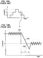
- a microstep driving in which in order to make the suppression of vibration at the time of rotation or the precise control of angle of rotation, a constant current flowing through the driving coil is step-wise changed, as shown in Fig. 13A, so that the rotor is transiently stopped at an angle smaller than the basic step angle.
- a current detecting resistor is inserted in an H-bridge circuit so that the amplitude of a current supplied from a power source to a stepping motor is detected as a detection voltage which the current detecting resistor outputs.
- the detection voltage is compared with a predetermined reference voltage to cause the turn-on/off of semiconductor switching elements so that a switching current 102 having a fixed amplitude, as shown in Fig. 13B is flown through a driving coil, thereby stopping the rotor at an angle finer than a basic step angle.
- the current detecting resistor inserted in the H-bridge circuit is connected such that a current regeneratively returned to the power source does not flow therethrough. Accordingly, it is not possible to detect the current flowing through the driving coil during a time when the switching current is decreased by the power source regeneration.
- the regenerative current is flown only during an estimated time T until the switching current reaches a predetermined value.
- the current flowing through the stepping motor may decrease to a smaller value than it is required, for example, as shown by a current amount indicated by reference numeral 104.
- the transfer to a steady operation for flowing a predetermined stepping current may be caused so that a current is supplied to the driving coil. This will cause the vibration of the stepping motor.
- the flywheel diode capable of being incorporated in a power IC having been popularized in recent years is a PN diode and has a long reverse recovery time (Trr).
- Trr reverse recovery time
- One object of the present invention made for the above-mentioned inconveniences of the prior art is to provide an inductive load driving method and an H-bridge circuit control device in which a noise eliminating filter is not required.
- Another object of the present invention is to provide an inductive load driving method and an H-bridge circuit control device in which when a switching current flowing through an inductive load is decreased, the decrease of the switching current down to a desired amplitude can be detected.
- a method is an inductive load driving method in which an H-bridge circuit constructed to cause the flow of a current to an inductive load in both of forward and reverse directions by four semiconductor switching elements and flywheel diodes respectively connected in reverse parallel to the semiconductor switching elements is used, a current detecting resistor is inserted in the H-bridge circuit so that a current supplied from a power source to the inductive load flows through the current detecting resistor, and a detection voltage outputted by the current detecting resistor at the time of turn-on of two of the semiconductor switching elements is compared with a predetermined reference voltage to cut off the turn-on of the semiconductor switching element(s) so that a switching current flowing through the inductive load is kept in a predetermined amplitude, and the inductive load driving method is characterized in that the detection voltage is ignored during a predetermined blanking period after the turn-on of the two of the semiconductor switching elements.
- a method is an inductive load driving method in which in an H-bridge circuit constructed to cause the flow of a current to an inductive load in both of forward and reverse directions by four semiconductor switching elements and flywheel diodes respectively connected in reverse parallel to the semiconductor switching elements, a current detecting resistor is inserted so that a current supplied from a power source to the inductive load flows through the current detecting resistor and a current regeneratively returned from the inductive load to the power source does not flow through the current detecting resistor, and a detection voltage outputted by the current detecting resistor at the time of turn-on of two of the semiconductor switching elements is compared with a predetermined reference voltage to cut off the turn-on of the semiconductor switching element(s) so that a switching current flowing through the inductive load is kept in a predetermined amplitude, and the inductive load driving method is characterized in that in the case where the switching current to be kept is decreased, the reference voltage is decreased to cut off all of the four semiconductor switching elements so that an energy stored in the
- a device is an H-bridge circuit control device in which in an H-bridge circuit constructed to cause the flow of a current to an inductive load in both of forward and reverse directions by four semiconductor switching elements and flywheel diodes respectively connected in reverse parallel to the semiconductor switching elements, a current detecting resistor is inserted so that a current supplied from a power source to the inductive load flows through the current detecting resistor and a current regeneratively returned from the inductive load to the power source does not flow through the current detecting resistor, and a detection voltage generated across the current detecting resistor is detected to change the turned-on states of the semiconductor switching element(s) to the turned-off states thereof so that the amplitude of a switching current flowing through the inductive load is kept in a predetermined level, and the H-bridge circuit control device is characterized in that the detection voltage is ignored during a predetermined blanking period after the change of two of the semiconductor switching elements to turned-on states.
- a device is an H-bridge circuit control device in which in an H-bridge circuit constructed to cause the flow of a current to an inductive load in both of forward and reverse directions by four semiconductor switching elements and flywheel diodes respectively connected in reverse parallel to the semiconductor switching elements, a current detecting resistor is inserted so that a current supplied from a power source to the inductive load flows through the current detecting resistor and a current regeneratively returned from the inductive load to the power source does not flow through the current detecting resistor, and a detection voltage generated across the current detecting resistor is detected, and the H-bridge circuit control device is characterized in that when an energy stored in the inductive load is regeneratively returned to the power source for decreasing the amplitude of the switching, two of the semiconductor switching elements are turned on at a predetermined period so that a current is supplied from the power source to the inductive load to generate the detection voltage, and the magnitude of the generated detection voltage is detected to judge whether or not the current flowing through the inductive load is decreased down to
- a current detecting resistor is inserted so that a current supplied from a power source to the inductive load flows through the current detecting resistor.
- a detection voltage outputted by the current detecting resistor at the time of turn-on of two of the semiconductor switching elements is compared with a predetermined reference voltage. If the detection voltage is larger than the predetermined reference voltage, the turn-on of the semiconductor switching element(s) is cut off. Thereby, an energy stored in the inductive load is released through the flywheel diode(s) so that a switching current flowing through the inductive load can be kept in a predetermined amplitude.
- the flywheel diodes are changed from forward bias states to reverse bias states. At this time, the diode characteristic of the flywheel diode will be lost only during Trr (reverse recovery time) of that diode so that a through current flows.
- the detection voltage When the through current flows through the current detecting resistor, the detection voltage will exceed the reference voltage notwithstanding that a small current is flowing through the inductive load. Therefore, after the turn-on of the two semiconductor switching elements, the detection voltage is ignored during a predetermined blanking period so that an erroneous operation caused by the through current is not caused. Thereby, a need to provide a noise eliminating filter is eliminated.
- a current path for releasing an energy stored in the inductive load is formed by one semiconductor switching element and one said flywheel diode so that the energy stored in the inductive load is consumed by a forward saturation voltage of the semiconductor switching element and a forward drop voltage of the flywheel diode.
- a current detecting resistor is inserted so that a current supplied from a power source to the inductive load flows through the current detecting resistor and a current regeneratively returned from the inductive load to the power source does not flow through the current detecting resistor.
- a detection voltage outputted by the current detecting resistor at the time of turn-on of two of the semiconductor switching elements is compared with a predetermined reference voltage to cut off the turn-on of the semiconductor switching element(s) so that a switching current flowing through the inductive load is kept in a predetermined amplitude.
- the reference voltage is decreased to cut off all of the four semiconductor switching elements.
- an energy stored in the inductive load is regeneratively returned to the power source, thereby making it possible to quickly decrease the amplitude of the switching current.
- reference numeral 3 denotes a stepping motor control apparatus which has an H-bridge circuit control device 2 according to an embodiment of the present invention and an H-bridge circuit 4.
- the H-bridge circuit 4 includes the H-bridge connection of PNP transistors Q 1 and Q 2 having flywheel diodes D 1 and D 2 respectively connected in reverse parallel thereto, NPN transistors Q 3 and Q 4 having flywheel diodes D 4 and D 3 connected in reverse parallel thereto, and an inductive load (or driving coil) L.
- the base terminals of the transistors Q 1 to Q 4 are connected to the H-bridge circuit control device 2.
- the H-bridge circuit control device 2 is constructed to cause the turn-on of any one of a set of PNP transistor Q 1 and NPN transistor Q 3 and a set of PNP transistor Q 2 and NPN transistor Q 4 so that a current is caused to be flown from a power source to the inductive load L in either a forward direction or a reverse direction, and it is constructed to cause the turn-off of the transistor having been turned on in that state so that an energy stored in the inductive load L causes a current to be flown through the flywheel diodes D 1 to D 4 .
- the transistors Q 1 to Q 4 , the flywheel diodes D 1 to D 4 and the H-bridge circuit control device 2 are formed in the same chip, thereby providing a one-chip power IC structure.
- a current detecting resistor R S constructed by discrete parts is inserted between the interconnected emitter terminals of the NPN transistors Q 3 and Q 4 and the interconnected cathode terminals of the flywheel diodes D 3 and D 4 .
- the cathode terminals of the flywheel diodes D 3 and D 4 are connected to a ground potential.
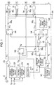
- the internal block diagram of the H-bridge circuit control device 2 is shown in Fig. 1.
- the H-bridge circuit control device 2 has a control circuit 5.
- the control circuit 5 includes two 3-input NAND circuits 32 and 31, two 2-input AND circuits 33 and 34, and inverters 30 1 and 30 2 .
- the output terminals of the 3-input NAND circuits 31 and 32 are connected to the base terminals of the PNP transistors Q 1 and Q 2 , respectively.
- the output terminals of the 2-input AND circuits 33 and 34 are connected to the base terminals of the NPN transistors Q 3 and Q 4 , respectively.
- a transistor selecting line 20 introduced from the exterior is connected to one of the input terminals of each of the 3-input NAND circuit 31 and the 2-input AND circuit 33.
- the transistor selecting line 20 is also connected to one of the input terminals of each of the 3-input NAND circuit 32 and the 2-input AND circuit 34 through the inverter 30 1 or 30 2 .
- the set of PNP transistor Q 1 and NPN transistor Q 3 are allowed to turn on but the set of PNP transistor Q 2 and NPN transistor Q 4 are not allowed to turn on.
- the signal is "LOW”
- the set of PNP transistor Q 2 and NPN transistor Q 4 are allowed to turn on but the set of PNP transistor Q 1 and NPN transistor Q 2 are not allowed to turn on. Accordingly, only one of the two sets is allowed to turn on so that the power source 9 is not short-circuited. In the following, it is assumed that the transistor selecting line 20 is "HIGH” and only the set of PNP transistor Q 1 and NPN transistor Q 3 are allowed to turn on.
- Inverters 30 3 and 30 4 are provided in the control circuit 5.
- An output terminal of the inverter 30 3 is connected to an input terminal of each of the 3-input NAND circuits 31 and 32 and the 2-input AND circuits 33 and 34.
- An output terminal of the inverter 30 4 is connected to the remaining input terminal of each of the 3-input NAND circuits 31 and 32. Accordingly, when the outputs of the inverters 30 3 and 30 4 are both "HIGH", the PNP transistor Q 1 and the NPN transistor Q 3 are both turned on so that a supply current 6 1 is supplied from the power source 9 to the inductive load L.
- the PNP transistor Q 1 When the output of the inverter 30 3 is turned into "LOW" from such a state, the PNP transistor Q 1 is turned off so that a back electromotive force generated across the opposite ends of the inductive load causes the flow of a commutation current 6 3 in a current path formed by the NPN transistor Q 3 , the current detecting resistor R S and the flywheel diode D 3 , as shown in Fig. 7. Thereby, an energy stored in the inductive load L is consumed as a heat.
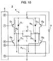
- the flywheel diode D 3 has a sudden change from a forward bias state to a reverse bias state. Therefore, the diode characteristic of the flywheel diode D 3 is lost only during a reverse recovery time Trr of the PN junction diode. As a result, a part of a current 6 4 flown through the PNP transistor Q 1 flows through the flywheel diode D 3 in a reverse direction and then to the ground as a through current 6 6 , as shown in Fig. 8.
- the H-bridge circuit control device 2 includes a comparator 24, a variable reference voltage circuit 22, a voltage change-over detecting circuit 23 and an oscillator 26 in addition to the above-mentioned control circuit 5.
- the outputs of the comparator 24, the variable reference voltage circuit 22, the voltage change-over detecting circuit 23 and the oscillator 26 are connected so that they are inputted to the control circuit 5.
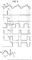
- the oscillator 26 is constructed such that a sawtooth wave V T as shown in a timing chart of Fig. 2 is outputted by a resistor and a condenser externally mounted.
- a sawtooth wave V T as shown in a timing chart of Fig. 2 is outputted by a resistor and a condenser externally mounted.
- the PNP transistor Q 1 and the NPN transistor Q 3 are turned off when the voltage of the sawtooth wave V T changes from the increase to the decrease. Accordingly, the current 6 1 begins to be supplied from the power source 9 to the inductive load L at a predetermined period.
- the PNP transistor Q 1 is turned off when the detection voltage V S exceeds a variable reference voltage V R which the variable reference voltage circuit 22 outputs.
- the commutation current 6 3 shown in Fig. 7 is flown so that the energy stored in the inductive load L is consumed.
- the control circuit 5 is provided with a reference voltage circuit 50, a negative edge detecting circuit 51, a positive edge detecting circuit 58, four FF's (flip-flops) 54 to 57, two 3-input NOR's 52 and 53 and inverters 30 5 and 30 6 in addition to the above-mentioned 3-input NAND circuit circuit 31 and so forth.
- the sawtooth wave V T outputted by the oscillator 26 is inputted to the negative edge detecting circuit 51.
- the negative edge detecting circuit 51 outputs a signal, as shown by symbol V 1 in Fig. 2, which becomes "HIGH” at the rising portion of the sawtooth wave V T and "LOW” at the falling portion thereof. This signal V 1 is inputted to the inverter 30 5 .
- the inverter 30 5 outputs an inverted version V 2 of the signal V 1 to the reset terminals R of the FF's 54 and 55.
- Each of the four flip-flops (or FF's 54 to 57) has two comparators 91 and 92 each including two NPN transistors and a constant current load, as shown in Fig. 11.
- the comparators 91 and 92 are constructed such that one input and one output are cross-connected. The remaining inputs are a set terminal S and a reset terminal R. Also, the output of the comparator 92 on the reset terminal R side is taken out as an output terminal Q to the exterior.
- the state of the output terminal Q is necessarily "LOW" in a state in which the reset terminal is "HIGH" (reset terminal preference).
- a relationship between the set and reset terminals S and R of each of the FF's 54 to 57 and the output terminal Q thereof is shown as a truth table by the following Table 1. It is not necessarily required that the FF's 54 to 57 should be constructed by bipolar transistors. They may be constructed by CMOS transistors so long as the operation is attained according to the truth table as shown in Fig. 12.
- the reset terminals R of the FF's 54 and 55 are kept in "HIGH” states and hence the output terminals Q thereof are kept in "LOW” states. Since the output terminal Q of the FF 54 is connected to the 3-input NAND circuit 31 and the 2-input AND circuit 33 through the inverter 30 3 , "HIGH” is inputted to the 3-input NAND circuit 31 and the 2-input AND circuit 33 during the time when the voltage of the sawtooth wave V T is increasing.
- the output terminal Q of the FF 56 is kept in a "HIGH” state, the "HIGH” signal outputted by the FF 56 is inputted to the 3-input NOR's 52 and 53 so that signals outputted by the 3-input NOR's 52 and 53 are kept “LOW” irrespective of the states of the remaining inputs.
- the inverter 30 3 continues to output "HIGH” to the 3-input NAND circuit 31 and the 2-input AND circuit 33.
- the selecting line 20 assumes a "HIGH” state.
- the 3-input NAND circuit 31 and the 2-input AND circuit 33 cause the turn-on of the PNP transistor Q 1 and the turn-on of the NPN transistor Q 3 , respectively, when all the input terminals of the NAND circuit 31 and all the input terminals of the AND circuit 33 are "HIGH". Therefore, the NPN transistor Q 3 remains turned on.
- the PNP transistor Q 1 is turned on when the output of the inverter 30 4 is "HIGH” or the output terminal Q of the FF 54 is "LOW” and is turned off when the output terminal Q of the FF 54 is "HIGH".
- the inverter 30 4 is inputted with a signal which the FF 55 outputs and is shown by symbol V 3 in Fig. 2.
- the reset terminal R of the FF 55 is inputted with the signal V 2 which the inverter 30 3 outputs. Accordingly, when the signal V 1 outputted by the negative edge detecting circuit 51 turns into “LOW” and hence the signal V 2 turns into “HIGH”, the reset terminal R of the FF 55 is raised. Thereby, the V 3 outputted by the FF 55 turns into "LOW” so that the transistor Q 1 is turned on.
- the set terminal S of the FF 55 is inputted with the output V C of the comparator 24. Further, a non-inverted input terminal of the comparator 24 is inputted with the detection voltage V S . Also, an inverted input terminal of the comparator 24 is inputted with the variable reference voltage V R which the variable reference voltage circuit 22 outputs.
- the output V C of the comparator 24 is "LOW" when the supply current 6 1 flowing through the current detecting resistor R S is still small so that the detection voltage V S is below the variable reference voltage V R .
- the output V C of the comparator 24 turns into "HIGH”. Accordingly, when the detection voltage V S exceeds the variable reference voltage V R , the set terminal S of the FF 55 is raised so that the output voltage V 3 turns into "HIGH”. At this time, the PNP transistor Q 1 is turned off.
- the flywheel diode having a PN junction formed in a one-chip power IC has the length of Trr equal to about 0.1 to 0.2 ⁇ sec.
- Trr the PNP transistor Q 1 makes an active operation. Therefore, during the lapse of Trr, the potential of one end of the stray capacitor C is changed from a potential lower than the ground potential by the forward drop voltage of the flywheel diode D 3 up to the power source voltage of the power source 9. Thereby, the rush current 6 5 flows until Trr expires. Accordingly, the width of the noise V N is the same as the length of Trr and the width of the pulse V P does not exceed the width of the noise V N .
- first blanking period B 1 the signal V 2 inputted to the reset terminal R of the FF 55 turns into "LOW” so that the FF 55 turns into an operable state, thereby enabling the turn-off of the PNP transistor Q 1 .
- the current 6 1 supplied from the power source 9 to the inductive load L increases.
- the output V C of the comparator 24 turns into "HIGH”. Thereby, the set terminal S of the FF 55 is raised so that the PNP transistor Q 1 is turned off.
- the NPN transistor Q 3 remains turned on. Accordingly, when the PNP transistor Q 1 is placed in the turned-off state, an energy stored in the inductive load L causes the flow of a commutation current 6 3 in a current path, as shown in Fig. 7, which is formed by the NPN transistor Q 3 and the flywheel diode D 3 . Thus, the energy is slowly attenuated while being consumed as a heat by the NPN transistor Q 3 and the flywheel diode D 3 .
- variable reference voltage V R is fixed.
- the signal V 3 outputted by the FF 55 turns into "LOW" at a fixed period to cause the turn-on of the PNP transistor Q 1 and the comparator 24 causes the turn-off of the PNP transistor Q 1 at a fixed period. Therefore, the supply current 6 1 supplied from the power source 9 and the commutation current 6 3 for releasing the stored energy alternately flow through the inductive load L so that a switching current formed thereby is kept in a fixed amplitude.
- variable reference voltage V R is decreased to decrease the switching current flowing through the inductive load L.
- a circuit for generating signals for changing over a reference voltage is provided at the exterior of the H-bridge circuit control device 2, and reference voltage change-over signals I 0 and I 1 outputted by the change-over signal generating circuit are inputted to the variable reference voltage circuit 22.
- Each of the reference voltage change-over signals I 0 and I 1 is a signal which takes two values of "HIGH” and "LOW".
- the variable reference voltage circuit 22 is constructed such that it can output a variable reference voltage V R having four kinds of magnitudes corresponding to the combination of the values of the reference voltage change-over signals I 0 and I 1 .
- the reference voltage change-over signals I 0 and I 1 are also inputted to the voltage change-over detecting circuit 23.
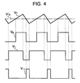
- the voltage change-over detecting circuit 23 detects a positive edge indicating the change from "LOW” to "HIGH” to outputs a pulse shown by symbol V 5 in Fig. 3.
- This pulse V 5 is inputted to the reset terminal R of the FF 56 so that a signal V 6 outputted from the output terminal Q of the FF 56 is changed from "HIGH” to "LOW”.
- This signal V 6 is inputted to the 3-input NOR's 52 and 53, thereby starting an operation for decreasing the switching current.
- the 3-input NOR 53 is inputted with the signal V 6 outputted by the FF 56 as well as the output V 8 of a comparator 59 and the signal V 1 outputted by the negative edge detecting circuit 51.
- the comparator 59 is constructed such that it has an inverted input terminal inputted with a reference voltage V' R outputted by the reference voltage circuit 50 and a non-inverted input terminal inputted with the sawtooth wave V T outputted by the oscillator 26 to compare the reference voltage V' R and the sawtooth wave V T and it provides the output V 8 of "HIGH” during a time when the sawtooth wave V T exceeds the reference voltage V' R . Since the signal V 6 is "low", a signal V 11 outputted by the 3-input NOR 53 turns into “HIGH” when both the output V 8 and the signal V 1 outputted by the negative edge detecting circuit 51 turn into “LOW", as shown in Fig. 4.
- the 3-input NOR 52 is inputted with the voltage V 6 outputted by the FF 56 as well as the output V 8 of the comparator 59 and a signal outputted by the inverter 30 6 which inverts the output V C of the comparator 24.
- the signal V 6 is "LOW". Accordingly, an output signal of the 3-input NOR 52 takes “LOW” when the output V 8 of the comparator 59 is "HIGH” and takes “HIGH” when the output V 8 of the comparator 59 is “LOW”. Namely, the 3-input NOR circuit 52 operates as an inverter for the comparator 59 in such a manner that an inverted version of the output V 8 or a signal shown by symbol V 9 in Fig. 3 is outputted to the set terminal S of the FF 54 and the reset terminal R of the FF 57.
- the reset terminal R of the FF 54 is inputted with the signal V 2 in a version of the output V 1 of the negative edge detecting circuit 51 inverted by the inverter 30 5 .
- the FF 54 is constructed such that the output terminal Q is always “LOW” in a state in which the reset terminal R is "HIGH". Therefore, as shown by symbol V 10 in Fig. 3, a signal outputted by the FF 54 takes "LOW” only during a time when the voltage of the sawtooth wave V T is decreasing.
- the signal V 9 outputted by the 3-input NOR 52 and the signal V 11 outputted by the 3-input NOR 53 are synchronous with each other. Therefore, when the set terminal S of the FF 57 is "HIGH”, the reset terminal R thereof is also "HIGH” and hence the output terminal Q of the FF 57 is kept “LOW".
- the signal V 10 outputted from the FF 54 is applied to the 3-input NAND circuit 31 and the 2-input AND circuit 33 after the inversion thereof by the inverter 30 3 .
- the signal V 3 outputted from the FF 55 is inputted to the 3-input NAND circuit 31 after the inversion thereof by the inverter 30 4 , the set terminal S of the FF 55 is kept in its "HIGH” state until the current flowing through the inductive load L finishes decreasing.
- the reset terminal R of the FF 55 is inputted with the signal V 2 which takes "HIGH” only during the time when the voltage of the sawtooth wave V T is decreasing. Since a preference to the input of the reset terminal R is made, the signal V 3 outputted by the FF 55 takes "LOW” during the time when the voltage of the sawtooth wave V T is decreasing. This signal V 3 is inputted to the 3-input NAND circuit circuit 31 after the inversion thereof by the inverter 30 4 .
- This detection voltage V S and the variable reference voltage V R are compared by the comparator 24, and the output V C as the result of comparison is inputted to the 3-input NOR 52 through the inverter 30 6 .
- the voltage of the sawtooth wave V T begins to decrease, that is, in the period of Trr from an instant of time when the PNP transistor Q 1 and the NPN transistor Q 3 are turned on, through currents 6 8 and 6 9 as shown in Fig. 10 will flow through the flywheel diodes D 1 and D 3 . Since the current 6 8 of the through currents 6 8 and 6 9 flows through the current detecting resistor R S , noises will be superimposed on the detection voltage V S . Especially, if such noises are generated when the current flowing through the inductive load L becomes sufficiently small so that the detection voltage V S is below the variable reference voltage V R , the noises make the circuit operation unstable.
- the output of the inverter 30 3 takes “HIGH” only during the period of time when the voltage of the sawtooth wave V T is decreasing. Therefore, in a period of time when the voltage of the sawtooth wave V T increases, that is, in a period of time when the signal V 10 is "HIGH”, the output of the inverter 30 3 is "LOW” and hence the PNP transistor Q 1 and the NPN transistor Q 3 are both turned on.
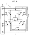
- a back electromotive force is generated by an energy stored in the inductive load L so that a regenerative current 67 flows in a path including the inductive load L, the flywheel diode D 2 , the power source 9 and the flywheel diode D 3 , as shown in Fig. 9. Since this regenerative current 6 7 charges an output condenser included in the power source 9, the energy released from the inductive load L moves toward the power source.
- the current is quickly attenuated.
- the regenerative current 6 7 does not pass through the current detecting resistor R S . Therefore, when the regenerative current 6 7 is flowing, the non-inverted terminal of the comparator 24 is connected to the ground potential through the current detecting resistor R S so that the output V C of the comparator 24 takes "LOW". Since the output V C is outputted to the 3-input NOR 52 through the inverter 30 6 , the output V 9 of the 3-input NOR 52 takes "LOW" when the regenerative current 67 is flowing. Accordingly, there is no fear that the set terminal S of the FF 54 is raised or the FF 57 is reset.
- the 3-input NOR 53 is inputted with the signal V 6 outputted by the FF 56, the signal V 1 outputted by the negative edge detecting circuit 51 and the signal V 8 outputted by the comparator 59 but the signal V 6 gives no influence upon the output of the 3-input NOR 53 since the signal V 6 remains "LOW” when the detection voltage V S is larger than the variable reference voltage V R . Accordingly, the signal V 11 outputted by the 3-input NOR 53 takes "LOW” when any one of the signal V 8 and the signal V 1 is "HIGH” and takes “HIGH” only when both of the signal V 8 and the signal V 1 are “LOW", as shown in Fig. 4.
- the signal V 11 takes "HIGH" when the voltage of the sawtooth wave V T is being lowered and when the voltage of the sawtooth wave V T is below the reference voltage V' R .
- the signal V 11 is inputted to the set terminal S of the FF 57
- the signal V 9 inputted to the reset terminal R of the FF 57 assumes "HIGH” in the same timing as the signal V 11 during a time when the inverter 30 6 continues to output "LOW". Therefore, the output terminal Q of the FF 57 remains "LOW".
- the positive edge detecting circuit 58 detects a positive edge indicating the change from "LOW” to "HIGH” to output a one pulse "HIGH” signal to the set terminal S of the FF 56.
- the output terminal Q of the FF 56 changes from "LOW” to "HIGH” which is in turn inputted to the 3-input NAND circuit circuit's 52 and 53. Accordingly, both of the outputs V 9 and V 11 of the 3-input NAND circuit circuit's 52 and 53 turn into “LOW”. After this, "LOW" is outputted irrespective of the states of the other input terminals of the 3-input NAND circuit circuits 54 and 57.
- the output terminal Q of the FF 56 remains "HIGH” so that the set terminal S of the FF 54 and the reset terminal R of the FF 57 are fixed in their "LOW” states. Therefore, the NPN transistor Q 3 remains in the turned-on state as mentioned earlier so that the switching current flowing through the inductive load L is kept in a fixed level by the turn-on/off of the PNP transistor Q 1 . In this case, an energy stored in the inductive load L is consumed by a commutation current 6 3 shown in Fig. 7.
- the present invention is not limited to the H-bridge circuit control device of the IC structure.
- An inductive load driving method and an H-bridge circuit control device for driving an H-bridge circuit using MOS transistors are also included in the present invention.
- the flywheel diode is not limited to the PN junction diode. Any flywheel diode to cause the flow of a rush current for the stray capacitor of the inductive load L may be included widely.
- a noise eliminating filter is not required, thereby reducing the cost.
- the second aspect of the invention when a switching current flowing through an inductive load is decreased, it is possible to detect whether or not the switching current is decreased down to a desired amplitude. Accordingly, there is no fear that the current flowing through the inductive load becomes too small or the transfer to a steady operation is caused while the current is large. Also, it is not required that a period of time for causing the flow of a regenerative current should be set again for each kind of stepping motors.
Landscapes
- Control Of Stepping Motors (AREA)
- Electronic Switches (AREA)
- Logic Circuits (AREA)
Priority Applications (1)
| Application Number | Priority Date | Filing Date | Title |
|---|---|---|---|
| EP03005262A EP1324493B1 (de) | 1996-05-02 | 1997-05-02 | Verfahren zur Speisung einer induktiven Last- und Steuereinrichtung für eine H-Brückenschaltung |
Applications Claiming Priority (3)
| Application Number | Priority Date | Filing Date | Title |
|---|---|---|---|
| JP135831/96 | 1996-05-02 | ||
| JP13583196 | 1996-05-02 | ||
| JP13583196A JP3665419B2 (ja) | 1996-05-02 | 1996-05-02 | 誘導性負荷駆動方法、及びhブリッジ回路制御装置 |
Related Child Applications (3)
| Application Number | Title | Priority Date | Filing Date |
|---|---|---|---|
| EP03005262A Division EP1324493B1 (de) | 1996-05-02 | 1997-05-02 | Verfahren zur Speisung einer induktiven Last- und Steuereinrichtung für eine H-Brückenschaltung |
| EP03005262.5 Division-Into | 2003-03-10 | ||
| EP04004525.4 Division-Into | 2004-02-27 |
Publications (3)
| Publication Number | Publication Date |
|---|---|
| EP0805555A2 true EP0805555A2 (de) | 1997-11-05 |
| EP0805555A3 EP0805555A3 (de) | 1998-09-09 |
| EP0805555B1 EP0805555B1 (de) | 2004-08-25 |
Family
ID=15160807
Family Applications (2)
| Application Number | Title | Priority Date | Filing Date |
|---|---|---|---|
| EP97107320A Expired - Lifetime EP0805555B1 (de) | 1996-05-02 | 1997-05-02 | Verfahren zur Speisung einer induktiven Last und Steuereinrichtung für eine H-Brückenschaltung |
| EP03005262A Expired - Lifetime EP1324493B1 (de) | 1996-05-02 | 1997-05-02 | Verfahren zur Speisung einer induktiven Last- und Steuereinrichtung für eine H-Brückenschaltung |
Family Applications After (1)
| Application Number | Title | Priority Date | Filing Date |
|---|---|---|---|
| EP03005262A Expired - Lifetime EP1324493B1 (de) | 1996-05-02 | 1997-05-02 | Verfahren zur Speisung einer induktiven Last- und Steuereinrichtung für eine H-Brückenschaltung |
Country Status (4)
| Country | Link |
|---|---|
| US (1) | US5952856A (de) |
| EP (2) | EP0805555B1 (de) |
| JP (1) | JP3665419B2 (de) |
| DE (2) | DE69730374T2 (de) |
Cited By (1)
| Publication number | Priority date | Publication date | Assignee | Title |
|---|---|---|---|---|
| EP2843831A3 (de) * | 2013-09-03 | 2016-01-20 | Kabushiki Kaisha Tokai Rika Denki Seisakusho | Motorantriebseinheit |
Families Citing this family (50)
| Publication number | Priority date | Publication date | Assignee | Title |
|---|---|---|---|---|
| JP3365250B2 (ja) * | 1997-04-28 | 2003-01-08 | 関西日本電気株式会社 | ステッピングモータ駆動装置 |
| FI109734B (fi) * | 1998-11-11 | 2002-09-30 | Abb Oy | Ohjainpiiri |
| JP2000217370A (ja) * | 1999-01-25 | 2000-08-04 | Mitsubishi Electric Corp | パルス幅変調方式によるic出力回路 |
| US6198335B1 (en) * | 1999-02-25 | 2001-03-06 | Stmicroelectronics, Inc. | Method and apparatus to drive the coil of a magnetic write head |
| DE19946242A1 (de) * | 1999-09-27 | 2001-04-05 | Grundfos As | Frequenzumrichter für einen Elektromotor |
| DE60022338T2 (de) * | 2000-07-12 | 2006-06-14 | Ami Semiconductor Belgium Bvba | Integrierter Sinusgenerator mit hoher Ausgangsleistung |
| JP2002305875A (ja) * | 2001-04-04 | 2002-10-18 | Toyota Motor Corp | 電圧変換装置 |
| US6781445B2 (en) * | 2001-04-13 | 2004-08-24 | Zeevo, Inc. | Low power large signal RF tuned buffer amplifier |
| JP2003047260A (ja) * | 2001-05-22 | 2003-02-14 | Aisin Seiki Co Ltd | インダクタンス負荷駆動用ブリッジ回路の駆動方法 |
| WO2003005545A1 (en) * | 2001-07-05 | 2003-01-16 | Di/Dt, Inc. | Inductor current sensing in isolated switching regulators and related methods |
| US6617913B1 (en) * | 2001-08-27 | 2003-09-09 | Unisys Corporation | Self-latching H-bridge system and apparatus |
| GB0200027D0 (en) * | 2002-01-02 | 2002-02-13 | Bae Systems Plc | Improvements relating to operation of a current controller |
| ATE484882T1 (de) * | 2002-01-17 | 2010-10-15 | Nxp Bv | Cmos-inverterschaltung |
| ATE306143T1 (de) * | 2002-01-30 | 2005-10-15 | Koninkl Philips Electronics Nv | System umfassend eine elektrische brücke zur erzeugung eines elektrischen signals für eine last und steuereinheit für ein solches system |
| JP4086102B2 (ja) * | 2002-12-25 | 2008-05-14 | ミネベア株式会社 | ステッピングモータの制御装置 |
| US6879128B2 (en) * | 2003-07-28 | 2005-04-12 | Ims Inc. | Method and apparatus for independently controlling each phase of a multi-phase step motor |
| CN100426637C (zh) * | 2003-08-16 | 2008-10-15 | 鸿富锦精密工业(深圳)有限公司 | 直流无刷马达 |
| US7110204B2 (en) * | 2004-07-22 | 2006-09-19 | Texas Instruments Incorporated | Process-insensitive write current generation for a HDD preamplifier writer equipped with parallel output resistive damping |
| TWI328350B (en) * | 2004-08-04 | 2010-08-01 | Delta Electronics Inc | Method for a driving circuit |
| TWI288526B (en) * | 2005-12-30 | 2007-10-11 | Yen Sun Technology Corp | Speed transmission control circuit of a brushless DC motor |
| DE102007026912B4 (de) * | 2007-06-12 | 2013-06-06 | Siemens Aktiengesellschaft | Vorrichtung und Verfahren zur Stromversorgung einer induktiven Last |
| JP5011585B2 (ja) * | 2007-07-03 | 2012-08-29 | 三菱電機株式会社 | 電力素子の駆動回路 |
| US8217616B2 (en) * | 2007-11-02 | 2012-07-10 | HJamilton Sundstrand Corporation | Electric motor control with buck boost converter |
| US7965126B2 (en) | 2008-02-12 | 2011-06-21 | Transphorm Inc. | Bridge circuits and their components |
| US8289065B2 (en) | 2008-09-23 | 2012-10-16 | Transphorm Inc. | Inductive load power switching circuits |
| JP2010081043A (ja) * | 2008-09-24 | 2010-04-08 | Oki Semiconductor Co Ltd | Hブリッジ回路 |
| US8730701B2 (en) * | 2009-02-12 | 2014-05-20 | Ecolab Usa Inc. | Driving circuit for powering a bi-directional load |
| JP5337533B2 (ja) * | 2009-02-27 | 2013-11-06 | セミコンダクター・コンポーネンツ・インダストリーズ・リミテッド・ライアビリティ・カンパニー | モータ駆動回路 |
| US7869226B2 (en) * | 2009-03-31 | 2011-01-11 | Tdk-Lambda Americas Inc. | Achieving ZVS in a two quadrant converter using a simplified auxiliary circuit |
| US8138529B2 (en) | 2009-11-02 | 2012-03-20 | Transphorm Inc. | Package configurations for low EMI circuits |
| US8816497B2 (en) * | 2010-01-08 | 2014-08-26 | Transphorm Inc. | Electronic devices and components for high efficiency power circuits |
| WO2011092864A1 (ja) * | 2010-02-01 | 2011-08-04 | トヨタ自動車株式会社 | 信号伝達装置 |
| US8624662B2 (en) | 2010-02-05 | 2014-01-07 | Transphorm Inc. | Semiconductor electronic components and circuits |
| JP5537272B2 (ja) * | 2010-06-07 | 2014-07-02 | ローム株式会社 | 負荷駆動回路装置及びこれを用いた電気機器 |
| US8786327B2 (en) | 2011-02-28 | 2014-07-22 | Transphorm Inc. | Electronic components with reactive filters |
| US8674757B2 (en) * | 2011-11-01 | 2014-03-18 | Neoenergy Microelectronic, Inc. | Switching system and method for control thereof |
| US9209176B2 (en) | 2011-12-07 | 2015-12-08 | Transphorm Inc. | Semiconductor modules and methods of forming the same |
| US8648643B2 (en) | 2012-02-24 | 2014-02-11 | Transphorm Inc. | Semiconductor power modules and devices |
| US8803246B2 (en) | 2012-07-16 | 2014-08-12 | Transphorm Inc. | Semiconductor electronic components with integrated current limiters |
| JP5653975B2 (ja) * | 2012-08-27 | 2015-01-14 | 株式会社東海理化電機製作所 | モータ制御装置 |
| US8941417B2 (en) * | 2013-02-28 | 2015-01-27 | Texas Instruments Incorporated | Output driver for energy recovery from inductor based sensor |
| US9059076B2 (en) | 2013-04-01 | 2015-06-16 | Transphorm Inc. | Gate drivers for circuits based on semiconductor devices |
| CN104252995B (zh) * | 2013-06-28 | 2019-06-14 | 王海 | 二极管触点保护复合开关的控制电路及继电器的控制方法 |
| US9537425B2 (en) | 2013-07-09 | 2017-01-03 | Transphorm Inc. | Multilevel inverters and their components |
| US9543940B2 (en) | 2014-07-03 | 2017-01-10 | Transphorm Inc. | Switching circuits having ferrite beads |
| US9590494B1 (en) | 2014-07-17 | 2017-03-07 | Transphorm Inc. | Bridgeless power factor correction circuits |
| US10200030B2 (en) | 2015-03-13 | 2019-02-05 | Transphorm Inc. | Paralleling of switching devices for high power circuits |
| US10319648B2 (en) | 2017-04-17 | 2019-06-11 | Transphorm Inc. | Conditions for burn-in of high power semiconductors |
| FR3075494B1 (fr) | 2017-12-19 | 2019-11-08 | Continental Automotive France | Procede de suppression au moins partielle des oscillations survenant a la fin d'une decharge en courant pour un pont en h |
| CN112968635A (zh) * | 2019-11-29 | 2021-06-15 | 圣邦微电子(北京)股份有限公司 | 一种感性负载续流过程中的开关管保护电路 |
Family Cites Families (10)
| Publication number | Priority date | Publication date | Assignee | Title |
|---|---|---|---|---|
| US4578650A (en) * | 1983-06-15 | 1986-03-25 | Watson Industries, Inc. | Resonance drive oscillator circuit |
| JPH0640423B2 (ja) * | 1986-10-13 | 1994-05-25 | 富士通株式会社 | 情報記憶装置の位置決め制御方式 |
| IT1215501B (it) * | 1987-05-18 | 1990-02-14 | Sgs Microelettronica Spa | Circuito a ponte a transistori moscon ricircolo veloce di corrente abassa diddipazione. |
| DE3718309A1 (de) * | 1987-05-21 | 1988-12-15 | Vdo Schindling | Schaltungsanordnung zur getakteten ansteuerung von halbleiterschaltern |
| JP2662803B2 (ja) * | 1988-09-30 | 1997-10-15 | 自動車機器株式会社 | 電気式動力舵取制御方法 |
| FR2645369A1 (fr) * | 1989-03-30 | 1990-10-05 | Alcatel Espace | Module de puissance pour electronique de commande de moteur continu |
| US4924158A (en) * | 1989-04-03 | 1990-05-08 | General Motors Corporation | Motor driver protection circuit |
| US5315498A (en) * | 1992-12-23 | 1994-05-24 | International Business Machines Corporation | Apparatus providing leading leg current sensing for control of full bridge power supply |
| US5359271A (en) * | 1993-01-25 | 1994-10-25 | Gtech Corporation | Microstepping bipolar stepping motor controller for document positioning |
| DE4327483A1 (de) * | 1993-08-16 | 1995-02-23 | Bosch Gmbh Robert | Verfahren und Vorrichtung zur Ansteuerung eines Leistungsstellelements einer Antriebseinheit eines Fahrzeugs |
-
1996
- 1996-05-02 JP JP13583196A patent/JP3665419B2/ja not_active Expired - Fee Related
-
1997
- 1997-04-30 US US08/841,384 patent/US5952856A/en not_active Expired - Lifetime
- 1997-05-02 DE DE69730374T patent/DE69730374T2/de not_active Expired - Fee Related
- 1997-05-02 DE DE69736363T patent/DE69736363T2/de not_active Expired - Fee Related
- 1997-05-02 EP EP97107320A patent/EP0805555B1/de not_active Expired - Lifetime
- 1997-05-02 EP EP03005262A patent/EP1324493B1/de not_active Expired - Lifetime
Cited By (1)
| Publication number | Priority date | Publication date | Assignee | Title |
|---|---|---|---|---|
| EP2843831A3 (de) * | 2013-09-03 | 2016-01-20 | Kabushiki Kaisha Tokai Rika Denki Seisakusho | Motorantriebseinheit |
Also Published As
| Publication number | Publication date |
|---|---|
| DE69736363D1 (de) | 2006-08-31 |
| EP0805555A3 (de) | 1998-09-09 |
| DE69730374D1 (de) | 2004-09-30 |
| JP3665419B2 (ja) | 2005-06-29 |
| DE69736363T2 (de) | 2007-07-12 |
| JPH09298455A (ja) | 1997-11-18 |
| EP1324493B1 (de) | 2006-07-19 |
| EP1324493A2 (de) | 2003-07-02 |
| EP0805555B1 (de) | 2004-08-25 |
| DE69730374T2 (de) | 2005-09-01 |
| EP1324493A3 (de) | 2003-07-09 |
| US5952856A (en) | 1999-09-14 |
Similar Documents
| Publication | Publication Date | Title |
|---|---|---|
| EP1324493B1 (de) | Verfahren zur Speisung einer induktiven Last- und Steuereinrichtung für eine H-Brückenschaltung | |
| EP0833439B1 (de) | Synchrones Antriebsverfahren für induktive Belastung und synchrone Steuereinrichtung für H-Brückenschaltung | |
| US5200878A (en) | Drive circuit for current sense igbt | |
| JP3665565B2 (ja) | 半導体集積回路およびモータ駆動制御システム | |
| US5200879A (en) | Drive circuit for voltage driven type semiconductor device | |
| US6285235B1 (en) | Gate control circuit for voltage drive switching element | |
| KR100623603B1 (ko) | 반도체장치 및 반도체장치 모듈 | |
| US3930170A (en) | Switching transistor drive apparatus | |
| US7622873B2 (en) | Motor drive device and drive method | |
| EP0208508A2 (de) | Pulsbreitenmodulationsansteuerschaltung | |
| US4434392A (en) | Circuit arrangement for controlling the commutation in a stepping motor | |
| US4684879A (en) | Transistor base drive circuit | |
| CN215222153U (zh) | 一种半导体开关器件退饱和检测电路及电机控制器 | |
| US4739190A (en) | Monolithically integratable high efficiency switching circuit | |
| KR101271882B1 (ko) | 모터 구동 장치 | |
| JPH07147726A (ja) | 半導体装置の過電圧制限回路 | |
| US6194951B1 (en) | Method and device for diving an integrated power output stage | |
| EP0746098B1 (de) | Impulsgenerator, Schaltung und Verfahren zur Ansteuerung von elektronischen Vorrichtungen und deren Verwendung | |
| JPH02262826A (ja) | 静電誘導形自己消弧素子の過電流検出方法および装置、それを用いた駆動回路とインバータ装置 | |
| JP2910175B2 (ja) | ブラシレスモータ | |
| US11876436B2 (en) | Voltage detecting apparatus and method for switching power converters | |
| JPH0710043B2 (ja) | Pwm駆動回路 | |
| JPS5825571A (ja) | 電子調整点火装置 | |
| JP3671796B2 (ja) | 電流制御型素子用駆動装置 | |
| JPS6249837B2 (de) |
Legal Events
| Date | Code | Title | Description |
|---|---|---|---|
| PUAI | Public reference made under article 153(3) epc to a published international application that has entered the european phase |
Free format text: ORIGINAL CODE: 0009012 |
|
| AK | Designated contracting states |
Kind code of ref document: A2 Designated state(s): DE FR IT |
|
| PUAL | Search report despatched |
Free format text: ORIGINAL CODE: 0009013 |
|
| AK | Designated contracting states |
Kind code of ref document: A3 Designated state(s): DE FR IT |
|
| 17P | Request for examination filed |
Effective date: 19990202 |
|
| 17Q | First examination report despatched |
Effective date: 20021209 |
|
| GRAP | Despatch of communication of intention to grant a patent |
Free format text: ORIGINAL CODE: EPIDOSNIGR1 |
|
| GRAS | Grant fee paid |
Free format text: ORIGINAL CODE: EPIDOSNIGR3 |
|
| GRAA | (expected) grant |
Free format text: ORIGINAL CODE: 0009210 |
|
| AK | Designated contracting states |
Kind code of ref document: B1 Designated state(s): DE FR IT |
|
| REF | Corresponds to: |
Ref document number: 69730374 Country of ref document: DE Date of ref document: 20040930 Kind code of ref document: P |
|
| ET | Fr: translation filed | ||
| PLBE | No opposition filed within time limit |
Free format text: ORIGINAL CODE: 0009261 |
|
| STAA | Information on the status of an ep patent application or granted ep patent |
Free format text: STATUS: NO OPPOSITION FILED WITHIN TIME LIMIT |
|
| 26N | No opposition filed |
Effective date: 20050526 |
|
| PGFP | Annual fee paid to national office [announced via postgrant information from national office to epo] |
Ref country code: IT Payment date: 20090521 Year of fee payment: 13 Ref country code: FR Payment date: 20090529 Year of fee payment: 13 |
|
| PGFP | Annual fee paid to national office [announced via postgrant information from national office to epo] |
Ref country code: DE Payment date: 20090730 Year of fee payment: 13 |
|
| REG | Reference to a national code |
Ref country code: FR Ref legal event code: ST Effective date: 20110131 |
|
| PG25 | Lapsed in a contracting state [announced via postgrant information from national office to epo] |
Ref country code: IT Free format text: LAPSE BECAUSE OF NON-PAYMENT OF DUE FEES Effective date: 20100502 |
|
| PG25 | Lapsed in a contracting state [announced via postgrant information from national office to epo] |
Ref country code: DE Free format text: LAPSE BECAUSE OF NON-PAYMENT OF DUE FEES Effective date: 20101201 |
|
| PG25 | Lapsed in a contracting state [announced via postgrant information from national office to epo] |
Ref country code: FR Free format text: LAPSE BECAUSE OF NON-PAYMENT OF DUE FEES Effective date: 20100531 |