EP0833439B1 - Synchrones Antriebsverfahren für induktive Belastung und synchrone Steuereinrichtung für H-Brückenschaltung - Google Patents
Synchrones Antriebsverfahren für induktive Belastung und synchrone Steuereinrichtung für H-Brückenschaltung Download PDFInfo
- Publication number
- EP0833439B1 EP0833439B1 EP97113903A EP97113903A EP0833439B1 EP 0833439 B1 EP0833439 B1 EP 0833439B1 EP 97113903 A EP97113903 A EP 97113903A EP 97113903 A EP97113903 A EP 97113903A EP 0833439 B1 EP0833439 B1 EP 0833439B1
- Authority
- EP
- European Patent Office
- Prior art keywords
- inductive load
- current
- power source
- period
- switching elements
- Prior art date
- Legal status (The legal status is an assumption and is not a legal conclusion. Google has not performed a legal analysis and makes no representation as to the accuracy of the status listed.)
- Expired - Lifetime
Links
- 230000001939 inductive effect Effects 0.000 title claims description 128
- 238000000034 method Methods 0.000 title claims description 23
- 230000001360 synchronised effect Effects 0.000 title description 3
- 230000008929 regeneration Effects 0.000 claims description 50
- 238000011069 regeneration method Methods 0.000 claims description 50
- 239000004065 semiconductor Substances 0.000 claims description 30
- 230000002441 reversible effect Effects 0.000 claims description 12
- 238000010586 diagram Methods 0.000 description 5
- 238000010276 construction Methods 0.000 description 4
- 230000001052 transient effect Effects 0.000 description 4
- 230000007423 decrease Effects 0.000 description 3
- 239000000758 substrate Substances 0.000 description 2
- 206010065929 Cardiovascular insufficiency Diseases 0.000 description 1
- 230000002238 attenuated effect Effects 0.000 description 1
- 230000003247 decreasing effect Effects 0.000 description 1
- 238000007599 discharging Methods 0.000 description 1
- 238000011084 recovery Methods 0.000 description 1
Images


Classifications
-
- H—ELECTRICITY
- H02—GENERATION; CONVERSION OR DISTRIBUTION OF ELECTRIC POWER
- H02P—CONTROL OR REGULATION OF ELECTRIC MOTORS, ELECTRIC GENERATORS OR DYNAMO-ELECTRIC CONVERTERS; CONTROLLING TRANSFORMERS, REACTORS OR CHOKE COILS
- H02P8/00—Arrangements for controlling dynamo-electric motors rotating step by step
- H02P8/12—Control or stabilisation of current
-
- H—ELECTRICITY
- H02—GENERATION; CONVERSION OR DISTRIBUTION OF ELECTRIC POWER
- H02P—CONTROL OR REGULATION OF ELECTRIC MOTORS, ELECTRIC GENERATORS OR DYNAMO-ELECTRIC CONVERTERS; CONTROLLING TRANSFORMERS, REACTORS OR CHOKE COILS
- H02P7/00—Arrangements for regulating or controlling the speed or torque of electric DC motors
- H02P7/03—Arrangements for regulating or controlling the speed or torque of electric DC motors for controlling the direction of rotation of DC motors
- H02P7/04—Arrangements for regulating or controlling the speed or torque of electric DC motors for controlling the direction of rotation of DC motors by means of a H-bridge circuit
Definitions
- the present invention relates to a technique of driving an inductive load by use of semiconductor switching elements, and more particularly to an inductive load driving method in which an H-bridge is formed to drive an inductive load and an inductive load driving apparatus which realizes such a method.
- a stepping motor is constructed such that it has a rotor including a rotatable moving magnet and a plurality of driving coils each including an electromagnet are arranged around the rotor.
- the position and the rotating speed of the rotor can be controlled in an open loop by selecting the driving coils to cause the flow of a pulse-like current having a predetermined amplitude.
- the stepping motors have widely been used as convenient motors.
- the stepping motor is an inductive load.
- a method for driving such a load there have widely been used a uni-polar driving method in which a current is flown in a fixed direction and a bi-polar driving system in which a current can be flown in either a forward direction or a reverse direction.
- each driving method is such that when a current supplied from a power source becomes equal to or larger than a predetermined value, a current is caused to flow through the flywheel diode connected in reverse parallel to the semiconductor switching element to release an energy stored in the inductive load, thereby attenuating the current flowing through the inductive load.
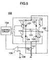
- FIG. 5 An example of such an inductive load driving method is shown in Fig. 5.
- reference numeral 102 denotes an inductive load driving apparatus according to the prior art in which an H-bridge circuit is formed by an inductive load 131 in a stepping motor and four transistors 111 to 114.
- the upper transistors 111 and 112 are connected to a power source 132, and the lower transistors 114 and 113 are connected to a ground potential through a current detecting resistor 133.
- Flywheel diodes 121 and 122 are connected in reverse parallel to the upper transistors 111 and 112, respectively. Similarly, flywheel diodes 123 and 124 are respectively connected in reverse parallel to the lower transistors 113 and 114 across the transistors 113 and 114 and the current detecting resistor 133.
- the base terminals of the transistors 111 to 114 are connected to a control circuit 134 so that the operation of the transistor is controlled by the control circuit 134.
- the transistors 111 and 113 are in turned-on conditions while the transistors 112 and 114 are in turned-off conditions.
- a supply current is supplied from the power source 132 to the inductive load 131 in a direction indicated by reference numeral 141.
- the supply current 141 flows through the current detecting resistor 133.
- a voltage generated across the current detecting resistor 133 becomes larger than a reference voltage 136
- the output of a comparator 135 is inverted and the control circuit 134 detects the inversion of the comparator output to stop the supply current 141, thereby attenuating the current flowing through inductive load 131.
- the control circuit 134 causes the flow of the supply current 141 from the power source 132 to the inductive load 131 again and stops the supply current 141 in accordance with the inversion of an output signal of the comparator 135. With the repetition of such an operation, a switching current flowing through the inductive load 131 can maintain a predetermined level.
- control circuit 134 stops the supply current 141 from the power source 132 to attenuate the current flowing through the inductive load 131.
- all of the transistors 111 to 114 are brought into turned-off conditions.
- the flywheel diodes 124 and 122 are reversely biased owing to an electromotive force generated in the inductive load 131 to cause the flow of a regeneration current indicated by reference numeral 142 in Fig. 6A.
- the flow of the regeneration current 142 causes the charging of (an output condenser of) the power source 132 so that a current flowing through the inductive load 131 is attenuated. In this case, it is possible to effectively utilize an energy stored in the inductive load 131.
- one of the transistors 111 and 113 is turned off.
- the transistor 111 is turned off with the transistor 113 being kept as it was turned on.
- the flywheel diode 124 is forwardly biased owing to a reverse electromotive force of the inductive load 131 to cause the flow of a commutation current indicated by reference numeral 143 in Fig. 6B.
- the flow of the commutation current 143 causes the generation of heat from the flywheel diode 124 and the transistor 113 so that an energy stored in the inductive load 131 is consumed to attenuate the current. In this case, it is not possible to utilize the energy stored in the inductive load 131.
- the regeneration current 142 can make the quick attenuation of a current flowing through the inductive load 131 at the time of switching of the current flowing through the inductive load 131 whereas the commutation current 143 can make the slow attenuation thereof.
- US-A-5,032,780 discloses a motor controller providing a digital monostable circuit which generates a control signal indicating whether a field coil within a motor should be turned on or off.
- Two registers are provided within the digital monostable to store values indicating a fixed off time and a minimum on time. These registers can be loaded with selected values by a microprocessor or other controller. The stored values are selectively loaded into a counter which, when the field coil current reaches a preselected level, turns the supply to the field coil off for a time corresponding to the off time value, then on again for a period at least as long as the minimum on time value.
- the values in the off time and minimum on time registers can be changed to suit operating conditions of the system, and the controller can be operated in either PWM or open loop mode.
- the present invention aims at the provision of a technique with which a switching current flowing through an inductive load can be controlled to the optimum by combining a regeneration current and a commutation current.
- Another object of the present invention is to provide a technique with which switching currents flowing through a plurality of inductive loads can be controlled to the optimum.
- an inductive load driving method for controlling a current flowing an inductive load, said current being supplied in both forward and reverse directions by an H-bridge circuit including four semiconductor switching elements and flywheel diodes respectively connected to said semiconductor switching elements, said inductive load driving method comprising at least two of a current supplying step of turning two of said semiconductor switching elements on so as to supply a current from a power source to said inductive load; a commutation step of turning one of said semiconductor switching elements on so that energy stored in said inductive load causes a current flowing through said one of said semiconductor switching elements and one of said flywheel diodes; and a power source regeneration step of turning all of said semiconductor switching elements off so that energy stored in said inductive load causes a current flowing through two of said flywheel diodes; wherein said inductive load driving method further comprises the step of generating a timing signal having a predetermined frequency and indicative of a driving period to (i) start said current supplying step in accordance with a start of said driving
- an inductive load driving apparatus comprising: an H-bridge circuit, including four semiconductor switching elements and flywheel diodes respectively connected to said semiconductor switching elements, for supplying a current in both forward and reverse directions through said inductive load; a control circuit for controlling said H-bridge circuit to perform at least two of (i) a current supplying operation of turning two of said semiconductor switching elements on so as to supply a current from a power source to said inductive load, (ii) a power source regeneration operation of turning one of said semiconductor switching elements on so that energy stored in said inductive load causes a current flowing through said one of said semiconductor switching elements and one of said flywheel diodes, and (iii) a commutation operation of turning all of said semiconductor switching elements off so that energy stored in said inductive load causes a current flowing through two of said flywheel diodes; and a timing signal generating circuit for generating a timing signal having a predetermined frequency and indicative of a driving period so that said control circuit controls said H-bridge circuit
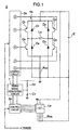
- reference numeral 2 denotes an example of an inductive load driving apparatus of the present invention for driving a two-phase stepping motor. It is assumed that an A-phase stepping motor is represented by an inductive load L A and a B-phase stepping motor is represented by an inductive load L B .
- This inductive load driving apparatus 2 includes an H-bridge circuit 4 A in which the inductive load L A is connected, an H-bridge circuit 4 B in which the inductive load L B is connected, control circuits 3 A and 3 B which control the H-bridge circuits 4 A and 4 B , respectively, and a timing signal generating circuit 7.
- the H-bridge circuits 4 A and 4 B , the control circuits 3 A and 3 B and the timing signal generating circuit 7 are formed as an IC structure on the same semiconductor substrate.
- Two current detecting resistors R SA and R SB , a timing resistor R T and a timing condenser C T as externally mounted parts constructed by discrete parts are connected to the inductive load driving apparatus.
- a series-connected circuit of the timing resistor R T and the timing condenser C T is connected between a power source voltage and a ground potential, and a voltage generated across the timing condenser C T is inputted to the timing signal generating circuit 7.
- a signal outputted by the timing signal generating circuit 7 is inputted to the control circuit 3 A and the control circuit 3 B .
- the control circuits 3 A and 3 B are connected to the H-bridge circuits 4 A and 4 B , respectively. With this construction, the inductive loads L A and L B are driven.
- the internal constructions of the H-bridge circuit 4 A and the H-bridge circuit 4 B are similar to each other. Also, the structures of the control circuit 3 A and the control circuit 3 B are similar to each other. Therefore, explanation will be made of the timing signal generating circuit 7, the control circuit 3 A which operates in accordance with a driving frequency generated by the timing signal generating circuit 7, and the A-phase stepping motor driving H-bridge circuit 4 A which is controlled by the control circuit 3 A while the explanation of the structures of the control circuit 3 B and the H-bridge circuit 4 B for B phase will be omitted.
- the H-bridge circuit 4 A includes transistors Q 1 to Q 4 which are semiconductor switching elements.
- the transistors Q 1 to Q 4 , flywheel diodes D 1 to D 4 and the control circuit 3 are formed on one semiconductor substrate.
- Two PNP transistors Q 1 and Q 2 are connected on the power source voltage side of a power source E, and two NPN transistors Q 3 and Q 4 are connected on the ground potential side.
- the PNP transistor Q 1 and the NPN transistor Q 4 are connected in series with each other while the PNP transistor Q 2 and the NPN transistor Q 3 are connected in series with each other.
- an H-bridge circuit can be formed by connecting the A-phase inductive load L A between the connected points of these series-connected circuits of the transistors.
- the above-mentioned current detecting resistor R SA is inserted between the NPN transistors Q 3 and Q 4 and the ground potential.
- the flywheel diodes D 3 and D 4 are respectively connected in reverse parallel to the NPN transistors Q 3 and Q 4 through the current detecting resistor R SA .
- the flywheel diodes D 1 and D 2 are directly connected in reverse parallel to the PNP transistors Q 1 and Q 2 , respectively.
- the base terminals ( 1 ⁇ to 4 ⁇ ) of the transistors Q 1 to Q 4 and a voltage output portion ( 5 ⁇ ) of the current detecting resistor R SA are connected to the control circuit 3 A .
- the control circuit 3 A brings any one of a set of the transistors Q 1 and Q 3 and a set of the transistors Q 2 and Q 4 into turned-on conditions in accordance with a PHASE signal inputted from the exterior to cause the flow of a current through the inductive load L A in a predetermined direction.
- the current supplied from the power source E to the inductive load L A flows through the current detecting resistor R SA so that a voltage corresponding to the amplitude of the current is generated. This voltage is detected to control a current flowing through the inductive load L A .
- the internal block of the control circuit 3A is shown in Fig. 2.
- the control circuit 3 A includes 2-input NAND 1 and NAND 2 and 2-input AND 3 and AND 4 .
- the respective output terminals ( 1 ⁇ , 2 ⁇ ) of the NAND 1 and NAND 2 are connected to the base terminals of the transistors Q 1 and Q 2
- the respective output terminals ( 3 ⁇ , 4 ⁇ ) of the AND 3 and AND 4 are connected to the base terminals of the transistors Q 3 and Q 4 .
- the above-mentioned PHASE signal inputted from the exterior is connected to the input terminals of the NAND 1 and AND 3 , as it is.
- the PHASE signal is connected to the input terminals of the NAND 2 and AND 4 through inverters INV 6 and INV 7 , respectively.
- the PHASE signal takes a high condition so that the turn-on of the transistors Q 2 and Q 4 is inhibited.
- the output conditions of the NAND 1 and AND 3 change in accordance with signals other than the PHASE signal, thereby controlling the transistors Q 1 and Q 3 .
- the control circuit 3 A has a reference power source VREF 1 for current comparison.
- the output of the reference VREF 1 and the output ( 5 ⁇ ) of the current detecting resistor R SA are inputted to an inverted input terminal and a non-inverted input terminal of a comparator COMP 1 , respectively, and an output terminal of the COMP 1 is connected to the set terminal S of each of flip-flops FF 1 and FF 2 .
- An output terminal Q of the FF 1 is connected to the input terminals of the NAND 1 and NAND 2 through an INV 2
- an output terminal Q of the FF 2 is connected to the input terminals of the AND 3 and 4 through an INV 3 .
- the FF 1 and FF 2 are constructed such that in a state in which the reset terminal R assumes a high condition, the output terminal Q takes a low condition irrespective of the condition of the set terminal S.
- the output voltage of the current detecting resistor R SA is below the output voltage of the reference power source VREF 1 , the output of the above-mentioned COMP 1 is low and hence the set terminals S of the FF 1 and FF 2 takes low conditions. Accordingly, the output terminals Q of the FF 1 and FF 2 are low. These low outputs are respectively inverted by the INV 2 and INV 3 so that the inverted high outputs are inputted to the NAND 1 and NAND 2 and the AND 3 and AND 4 , respectively.
- the transistors Q 1 and Q 3 are turned on so that a current is supplied from the power source E to the inductive load L A .
- the FF 1 and FF 2 are constructed such that the condition of the output terminal Q can be controlled in accordance with the condition of the reset terminal R even if the set terminal S takes a high condition.
- the reset terminals R of the FF 1 and FF 2 are connected to the output terminals of the timing signal generating circuit 7. As a result, the output terminals Q of the FF 1 and FF 2 are controlled by the timing signal generating circuit 7 when the output of the COMP 1 is high.
- the timing signal generating circuit 7 has an oscillator OSC, a comparator COMP 2 , a reference power source VREF 2 and an OR 1 and a connection is made such that the voltage of the above-mentioned timing condenser C T is inputted to the OSC.
- the OSC has a circuit incorporated therein for charging and discharging the timing condenser C T .
- a sawtooth wave oscillating at a fixed period as shown by reference numeral 21 in Fig. 3 is formed by the timing condenser C T (at a wiring portion indicated by reference symbol A).
- One period of the sawtooth wave 21 is defined as a driving period T.
- the generated rectangular wave 22 is outputted from the OSC (at a wiring portion indicated by reference symbol B) to the control circuit 3 A (and the control circuit 3 B ) and one input terminal of the OR 1 .
- the sawtooth wave 21 is also outputted to a non-inverted terminal of the COMP 2 , and an inverted terminal of the COMP 2 is inputted with a reference voltage outputted by the reference power source VREF 2 .
- the COMP 2 compares the inputted sawtooth wave 21 and the reference voltage to generate a rectangular wave 23 which is high when the sawtooth wave 21 is larger than the output voltage of VREF 2 and low when the former is smaller than the latter.
- the generated rectangular wave 23 is outputted from the COMP 2 to the other input terminal of the OR 1 (at a wiring portion indicated by reference symbol C).
- the OR 1 inputted with the rectangular wave 23 and the rectangular wave 24 performs the operation of addition of the rectangular waves 23 and 24 to generate a rectangular wave 24 which is in turn outputted to the control circuit 3 A and the control circuit 3 B (at a wiring portion indicated by reference symbol D).
- the rectangular waves 22 to 24 are generated from the waveform of the sawtooth wave 21 and by the comparison of the sawtooth wave 21 and the output voltage of the VREF 2 .
- the oscillating period of each of the rectangular waves 22 to 24 is the driving period T.
- the above-mentioned rectangular wave 22 and rectangular wave 24 are respectively inputted to the reset terminals R of the FF 1 and FF 2 in the control circuit 3 A (and the control circuit 3 B ), and the conditions of the set terminals S of the FF 1 and FF 2 are changed in accordance with the output of the COMP 1 .
- the transistors Q 1 and Q 3 are controlled by the COMP 2 and the timing signal generating circuit 7 through the FF 1 and FF 2 .
- the transistors Q 1 and Q 3 are both turned on so that there is performed a current supply operation in which a current is supplied from the power source E to the inductive load L A .
- the output terminal Q takes the low condition irrespective of the condition of the set terminal S. Therefore, during the time when the rectangular wave 22 is high, the output terminals Q of the FF 1 and FF 2 take the low conditions irrespective of whether the condition of the output signal of the COMP 1 is high or low, that is, in either the case where a voltage generated across the current detecting resistor R SA exceeds the output voltage of the VREF 1 or the case where the former voltage is below the latter voltage. As a result, the turned-on conditions of the transistors Q 1 and Q 3 are kept.
- the forced turn-on period corresponds to a period of time when the voltage of the sawtooth wave 21 attenuates. Also, the forced turn-on period corresponds to an initial stage of start of the current supply operation.
- the initial period of start of the current supply operation is taken as the forced turn-on period, thereby ignoring the output of the COMP 1 . Therefore, even in the case where the output of the COMP 1 is inverted by the noises, there is no fear that an erroneous operation of erroneously stopping the current supply operation is generated.
- the rectangular wave 22 and the rectangular wave 24 turn into low conditions and hence the reset terminals R of the FF 1 and FF 2 are brought into low conditions.
- the condition of the output terminal Q of the FF 1 or FF 2 is determined in accordance with the condition of the set terminal S when the condition of the reset terminal R is low. Accordingly, in the case where the output of the COMP 1 has taken a high condition as the result of the increase of a current supplied from the power source E in the compulsory turn-on period, the output terminals Q of the FF 1 and FF 2 immediately turn into high conditions, thereby bringing the transistors Q 1 and Q 3 into turned-off conditions.
- a power source regeneration period a period of time from the start of a compulsory turn-on period until the turn of the rectangular wave 24 from a low condition into a high condition
- a commutation period a period of time from the turn of the rectangular wave 24 into the high condition until the start of a forced turn-on period in the next driving period T.
- the output terminal Q of the FF 2 turns from a low condition into a high condition and hence the transistor Q 3 is also turned off so that a power source regeneration operation is'started.
- the transistor Q 3 is turned on again so that the power source regeneration operation transfers to a commutation operation.
- the output of the COMP 1 in the control circuit 3A is first inverted from a low condition to a high condition at the point of time P12 when the current I LA flowing through the inductive load L A reaches IREF A .
- the set terminals S of the FF 1 and FF 2 in the control circuit 3 A turn into a high condition.
- the reset terminals R of the FF 1 and FF 2 in the control circuit 3 A (and the control circuit 3 B ) assume low conditions. Therefore, at the point of time when the set terminal S turns into the high condition, the output terminal Q turns from a low condition into a high condition so that the transistors Q 1 and Q 3 in the H-bridge circuit 4 A are both brought into turned-off conditions.
- the flywheel diodes D 4 and D 2 in the H-bridge circuit 4 A are forwardly biased owing to an electromotive force generated in the inductive load L A so that a regeneration current flows from the ground potential side toward the power source E through the two flywheel diodes D 4 and D 2 .
- a power source regeneration operation an energy stored in the inductive load L A transfers to the power source E, thereby effectively utilizing the energy stored in the inductive load L A .
- the regeneration current flowing through the inductive load L A during the power source regeneration operation does not pass through the current detecting resistor R SA . Accordingly, during the power source regeneration period, zero (V) is inputted to the non-inverted input terminal of the COMP 1 in the control circuit 3 A and the output of the COMP 1 takes a low condition.
- the conditions of the reset terminals R of the FF 1 and FF 2 remain as they were low and hence the FF 1 and FF 2 maintain the original conditions until they are reset by the turn of the reset terminal R into a high condition. Therefore, the conditions of the output terminals Q of the FF 1 and FF 2 in the control circuit 3 A remain as they were high so that the transistors Q 1 and Q 3 maintain the turned-off conditions.
- the flywheel diode D 2 is reversely biased. Thereby, the direction of the regeneration current having flowing from the ground potential side to the power source E is changed so that a commutation current flows in a closed path formed by the inductive load L A , the transistor Q 3 , the current detecting resistor R SA and the flywheel diode D 4 .
- control circuit 3 B for driving the B-phase inductive load L B is also inputted with the above-mentioned rectangular waves 22 and 24, and the compulsory turn-on period, the power source regeneration period and the commutation period of the control circuit 3 B coincide with those of the control circuit 3 A .
- the transistor Q 1 in the H-bridge circuit 4 B turns from the turned-on condition into a turned-off condition and the transistor Q 3 therein maintains the turned-on condition, so that the transfer to a commutation operation is made with no power source regeneration operation being performed.
- the FF 1 is also reset so that the output terminal Q thereof takes a low condition.
- the transistors Q 1 in the H-bridge circuits 4 A and 4 B are simultaneously brought into turned-on conditions. With the turned-on transistors Q 1 and the transistors Q 3 having maintained the turned-on conditions, both the A-phase and B-phase H-bridge circuits 4 A and 4 B transfer to their current supply operations so that currents begin to be supplied from the power source E to the inductive loads L A and L B .
- FIG. 3 shows that after a current supply operation is performed again, the current I LA flowing through the A-phase inductive load L A reaches the upper limit current IREF A at a point P 15 after the lapse of a forced turn-on period so that the transfer to a power source regeneration operation is made at that time.
- the current I LB flowing through the B-phase inductive load L B already exceeds the upper limit current IREF B value at a point of time before the completion of a forced turn-on period and hence the transfer to a power source regeneration operation is made immediately at the point of time of the completion of the forced turn-on period.
- the start of a current supply operation for the A-phase inductive load L A and the start of a current supply operation for the B-phase inductive load L B are determined by the time constant of one series circuit of the timing resistor R T and the timing condenser C T and one timing signal generating circuit 7 and are therefore simultaneous with each other. Accordingly, there is no fear that the timings of start of both the current supply operations deviate from each other. As a result, there is no fear that noises or vibrations caused by beats are generated.
- the above-mentioned series of operations concern the case where currents flown to the inductive loads L A and L B are switched to keep the values thereof constant.
- the amplitudes of switching currents flown to the inductive loads L A and L B can be changed by changing the output voltages of the reference power sources VREF 1 and VREF 2 for current comparison in the control circuits 3 A and 3 B .
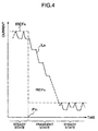
- Each of the current levels IREF A and IREF' A is a current value with which the output of the COMP 1 in the control circuit 3 A is inverted. Assume that at a point of time of completion of a compulsory turn-on period, a current flowing through the inductive load L A has already exceeded IREF' A and the COMP 1 has taken a high condition. At the point of time of completion of the forced turn-on period, the transfer to a power source regeneration operation is immediately made. When there turns into a commutation period, the transfer from the power source regeneration operation to a commutation operation is made.
- the driving period T follows the oscillating period of the sawtooth wave 21 as in the steady state with no difference between the transient state and the steady state.
- the operations for the A and B phases are synchronous with each other so that a current supply operation, a power source regeneration operation and a commutation operation for the A phase are started simultaneously with those for the B phase, respectively.
- bi-polar transistors are used as the semiconductor switching elements.
- insulated gate transistors MOSFET's
- the flywheel diodes may include various rectifying elements such as pn junction diodes, Schottky diodes or the like.
- the present invention may include a multi-chip module having the transistors Q 1 to Q 4 and the flywheel diodes D 1 to D 4 as single chips and a hybrid IC.
- timing resistor R T and the current detecting resistor R S incorporated therein may also be included in the present invention.
Landscapes
- Engineering & Computer Science (AREA)
- Power Engineering (AREA)
- Control Of Stepping Motors (AREA)
Claims (6)
- Induktions-Last-Treiberverfahren zum Steuern eines in einer induktiven Last (La) fließenden Stroms, wobei der Strom sowohl in der Vorwärts- als auch Rückwärtsrichtung durch eine H-Brückenschaltung (4A) geliefert wird, die vier Halbleiterschaltelemente (Q1-Q4) und Flywheel-Dioden (P1-D4) aufweist, die jeweils mit den Halbleiterschaltelementen verbunden sind, wobei das Induktions-Last-Treiberverfahren mindestens zwei der folgenden Schritte umfasst:wobei das Induktions-Last-Treiberverfahren ferner den Schritt eines Erzeugens eines Timing-Signals (A) mit einer vorbestimmten Frequenz umfasst, das eine Treiberperiode angibt, um (i) den Stromversorgungsschritt zu beginnen, in Übereinstimmung mit einem Beginn der Treiberperiode, und um den Stromversorgungsschritt anzuhalten, wenn eine Amplitude des durch die induktive Last fließenden Stroms einen vorbestimmten Wert oder mehr annimmt, um (ii) den Leistungsquellenregenerierungsschritt zu beginnen, wenn der Stromversorgungsschritt vor einem vorbestimmten Zeitpunkt angehalten wird, und um den Leistungsquellenregenerierungsschritt bei der vorbestimmten Zeitspanne anzuhalten, und um (iii) den Kommutierungsschritt zu beginnen, wenn der Stromversorgungsschritt oder der Stromversorgungsschritt angehalten wird, und um den Kommutierungsschritt am Ende der Treiberperiode anzuhalten.einen Stromversorgungsschritt zum Anschalten von zwei der Halbleiterschaltelemente, um einen Strom von einer Leistungsquelle (E) an die induktive Last (LA) zu liefern;einen Kommutierungsschritt zum Anschalten eines der Halbleiterschaltelemente, so dass die in der induktiven Last gespeicherte Energie bewirkt, dass ein Strom durch eines der Halbleiterschaltelemente und eine der Flywheel-Dioden fließt; undeinen Leistungsquellenregenerierungsschritt eines Abschaltens aller Halbleiterschaltelemente, so dass die in der induktiven Last gespeicherte Energie bewirkt, dass ein Strom durch zwei der Flywheel-Dioden fließt;
- Induktions-Last-Treiberverfahren gemäß Anspruch 1 zum Steuern einer Mehrzahl von durch induktive Lasten (LA, LB) fließenden Strömen, wobei die Ströme jeweils von einer Mehrzahl von H-Brückenschaltungen (4A,4B) geliefert werden,
wobei die Mehrzahl der H-Brückenschaltungen mit der gleichen Treiberperiode angetrieben werden. - Induktions-Last-Treiberverfahren gemäß Anspruch 1 der 2, bei dem der Stromversorgungsschritt in einer vorbestimmten Zeitspanne vom Beginn der Treiberperiode, ungeachtet der Amplitude des durch die induktive Last fließenden Stroms, fortgesetzt wird.
- Vorrichtung zum Treiben einer induktiven Last mit:einer H-Brückenschaltung (4A), die vier Halbleiterschaltelemente (Q1-Q4) und Flywheel-Dioden (D1-D4) aufweist, die jeweils mit den Halbleiterschaltelementen verbunden sind, zum Liefern eines Stroms in sowohl der Vorwärts- als auch der Rückwärtsrichtung durch die induktive Last;eine Steuerschaltung (3A) zum Steuern der H-Brückenschaltung, um mindestens zwei der folgenden Vorgänge durchzuführen: (i) einen Stromversorgungsvorgang mit einem Anschalten von zwei der Halbleiterschaltelemente, um einen Strom einer Leistungsquelle an die induktive Last zu liefern, (ii) einen Leistungsquellenregenerierungsvorgang mit einem Einschalten eines der Halbleiterschaltelemente, so dass die in der induktiven Last gespeicherte Energie veranlasst, dass ein Strom durch eines der Halbleiterschaltelemente und eine der Flywheel-Dioden fließt, und (iii) einen Kommutierungsvorgang mit dem Abschalten aller Halbleiterschaltelemente, so dass die in der induktiven Last in der induktiven Last gespeicherte Energie veranlasst, dass ein Strom durch zwei der Flywheel-Dioden fließt; undeiner Timing-Signalerzeugungsschaltung (7) zum Erzeugen eines Timing-Signals mit einer vorbestimmten Frequenz, das eine Treiberperiode angibt, so dass die Steuerschaltung die H-Brückenschaltung steuert, um (i) den Stromversorgungsvorgang in Übereinstimmung mit einem Anfang der Treiberzeitspanne zu beginnen, und um den Stromversorgungsvorgang anzuhalten, wenn eine Amplitude des durch die induktive Last fließenden Stroms einen vorbestimmten Wert oder mehr annimmt, um (ii) den Leistungsquellenregenerierungsvorgang zu beginnen, wenn der Stromversorgungsvorgang vor einem vorbestimmten Zeitpunkt angehalten wird, und den Leistungsquellenregenerierungsvorgang bei der vorbestimmten Periode anzuhalten und um (iii) den Kommutierungsvorgang zu beginnen, wenn der Stromversorgungsvorgang oder der Stromversorgungsvorgang angehalten wird, und den Kommutierungsvorgang am Ende der Treiberperiode anzuhalten.
- Vorrichtung zum Treiben einer induktiven Last gemäß Anspruch 4, mit einer Mehrzahl von H-Brückenschaltungen (4A,4B) zum jeweiligen Liefern von Strömen durch eine Mehrzahl jeweiliger induktiver Lasten (LA, LB), wobei die Mehrzahl der H-Brückenschaltungen mit der gleichen Treiberperiode betrieben werden.
- Vorrichtung zum Treiben einer induktiven Last gemäß Anspruch 4 oder 5, bei der der Stromversorgungsvorgang in einer vorbestimmten Zeitspanne von dem Beginn der Treiberperiode ungeachtet der Amplitude des durch die induktive Last fließenden Stroms fortgesetzt wird.
Applications Claiming Priority (3)
| Application Number | Priority Date | Filing Date | Title |
|---|---|---|---|
| JP25245196 | 1996-09-03 | ||
| JP25245196A JP3764784B2 (ja) | 1996-09-03 | 1996-09-03 | 誘導性負荷の同期駆動方法、及びhブリッジ回路の同期制御装置 |
| JP252451/96 | 1996-09-03 |
Publications (2)
| Publication Number | Publication Date |
|---|---|
| EP0833439A1 EP0833439A1 (de) | 1998-04-01 |
| EP0833439B1 true EP0833439B1 (de) | 2002-12-11 |
Family
ID=17237571
Family Applications (1)
| Application Number | Title | Priority Date | Filing Date |
|---|---|---|---|
| EP97113903A Expired - Lifetime EP0833439B1 (de) | 1996-09-03 | 1997-08-12 | Synchrones Antriebsverfahren für induktive Belastung und synchrone Steuereinrichtung für H-Brückenschaltung |
Country Status (4)
| Country | Link |
|---|---|
| US (1) | US6066930A (de) |
| EP (1) | EP0833439B1 (de) |
| JP (1) | JP3764784B2 (de) |
| DE (1) | DE69717754T2 (de) |
Families Citing this family (32)
| Publication number | Priority date | Publication date | Assignee | Title |
|---|---|---|---|---|
| JP3826499B2 (ja) * | 1997-06-27 | 2006-09-27 | アイシン精機株式会社 | 電気モータの通電制御装置 |
| US6978281B1 (en) * | 2000-11-21 | 2005-12-20 | Microsoft Corporation | Versioned project data |
| DE10120705A1 (de) * | 2001-04-27 | 2002-11-14 | Stribel Gmbh | Ansteuerung für Halbbrücke |
| US6807073B1 (en) * | 2001-05-02 | 2004-10-19 | Oltronics, Inc. | Switching type power converter circuit and method for use therein |
| US6806675B2 (en) | 2001-10-04 | 2004-10-19 | Abbott Laboratories | Stepper motor controller |
| JP3711102B2 (ja) * | 2002-10-30 | 2005-10-26 | 三洋電機株式会社 | 単相モータ駆動装置、単相モータ駆動方法、および集積回路 |
| JP3899071B2 (ja) | 2003-12-19 | 2007-03-28 | 松下電器産業株式会社 | ステッピングモータ駆動装置、及びステッピングモータ駆動方法 |
| US20090190280A1 (en) * | 2004-01-09 | 2009-07-30 | Mitsuaki Daio | Current limiter circuit and motor drive circuit |
| US6943514B1 (en) | 2004-04-06 | 2005-09-13 | Aimtron Technology Corp. | Motor control circuit for supplying a controllable driving current |
| JPWO2005112230A1 (ja) * | 2004-05-18 | 2008-05-15 | セイコーエプソン株式会社 | 電動機 |
| US7208893B2 (en) | 2005-01-11 | 2007-04-24 | Alps Electric Co., Ltd. | Motor driving control device to be driven at interval of constant time |
| JP4678668B2 (ja) * | 2005-03-08 | 2011-04-27 | ローム株式会社 | ステッピングモータ駆動回路及びそれを用いたステッピングモータ装置 |
| US7923955B2 (en) * | 2005-08-03 | 2011-04-12 | GM Global Technology Operations LLC | Method and apparatus for controlling an active engine mount |
| JP2007221974A (ja) * | 2006-02-20 | 2007-08-30 | Rohm Co Ltd | ステッピングモータ駆動装置および方法ならびにそれらを用いた電子機器 |
| TWI323077B (en) * | 2006-09-26 | 2010-04-01 | Holtek Semiconductor Inc | Driving apparatus for single phase motors and driving method thereof |
| KR101173923B1 (ko) * | 2007-07-03 | 2012-08-16 | 미쓰비시덴키 가부시키가이샤 | 전력소자의 구동회로 |
| JP2009065806A (ja) * | 2007-09-10 | 2009-03-26 | Panasonic Corp | ステッピングモータ駆動装置及びステッピングモータ駆動方法 |
| DE102009005702A1 (de) * | 2008-01-29 | 2009-07-30 | Ebm-Papst St. Georgen Gmbh & Co. Kg | Elektronisch kommutierter Motor |
| US8659259B2 (en) * | 2009-09-04 | 2014-02-25 | Canon Kabushiki Kaisha | Stepping motor driving apparatus |
| CN102910085B (zh) * | 2012-10-23 | 2014-08-13 | 西南交通大学 | 一种用于电磁吸力悬浮系统的双管独立交错控制方法 |
| US20150194915A1 (en) * | 2014-01-05 | 2015-07-09 | Makerbot Industries, Llc | H-bridge shoot-through avoidance |
| JP6322134B2 (ja) * | 2014-12-26 | 2018-05-09 | ミネベアミツミ株式会社 | モータ制御装置およびモータ制御方法 |
| JP6204385B2 (ja) * | 2015-01-22 | 2017-09-27 | ミネベアミツミ株式会社 | モータ電流制御装置およびモータ電流制御方法 |
| JP6204386B2 (ja) * | 2015-01-28 | 2017-09-27 | ミネベアミツミ株式会社 | モータ電流制御装置およびモータ電流制御方法 |
| JP6272797B2 (ja) | 2015-05-27 | 2018-01-31 | ミネベアミツミ株式会社 | モータ駆動制御装置およびモータ駆動制御方法 |
| JP6272798B2 (ja) | 2015-06-05 | 2018-01-31 | ミネベアミツミ株式会社 | モータ駆動制御装置およびモータ駆動制御方法 |
| JP2017041951A (ja) * | 2015-08-18 | 2017-02-23 | 株式会社東芝 | モータ駆動制御装置 |
| CN205545047U (zh) * | 2015-12-31 | 2016-08-31 | 峰岹科技(深圳)有限公司 | 感应电机驱动系统 |
| DE102017118837A1 (de) * | 2017-08-17 | 2019-02-21 | Trinamic Motion Control Gmbh & Co. Kg | Verfahren und Schaltungsanordnung zur Resonanzdämpfung bei Schrittmotoren |
| JP2022088079A (ja) * | 2020-12-02 | 2022-06-14 | 東芝三菱電機産業システム株式会社 | 電磁石電源装置 |
| TWI905567B (zh) * | 2023-11-09 | 2025-11-21 | 奇鋐科技股份有限公司 | 風扇剎車電路 |
| US12497972B2 (en) | 2023-11-21 | 2025-12-16 | Asia Vital Components Co., Ltd. | Fan brake circuit |
Family Cites Families (8)
| Publication number | Priority date | Publication date | Assignee | Title |
|---|---|---|---|---|
| US4368411A (en) * | 1981-07-13 | 1983-01-11 | Kollmorgen Technologies Corporation | Control system for electric motor |
| US4528486A (en) * | 1983-12-29 | 1985-07-09 | The Boeing Company | Controller for a brushless DC motor |
| EP0196543A3 (de) * | 1985-03-28 | 1988-01-13 | Kollmorgen Technologies Corporation | Stromregelung für eine induktive Last |
| US5032780A (en) * | 1989-09-29 | 1991-07-16 | Sgs-Thomson Microelectronics, Inc. | Programmable stepper motor controller |
| JP3354633B2 (ja) * | 1993-06-25 | 2002-12-09 | 富士通テン株式会社 | ステッピングモータ駆動装置 |
| US5578911A (en) * | 1994-09-21 | 1996-11-26 | Chrysler Corporation | Method and apparatus for power regeneration in an electric vehicle motor drive using a deadtime generator and having continuously variable regeneration control |
| US5703456A (en) * | 1995-05-26 | 1997-12-30 | Emerson Electric Co. | Power converter and control system for a motor using an inductive load and method of doing the same |
| US5602452A (en) * | 1995-09-19 | 1997-02-11 | Moog Inc. | Regeneration current-spike limiter for six-step motor drives |
-
1996
- 1996-09-03 JP JP25245196A patent/JP3764784B2/ja not_active Expired - Lifetime
-
1997
- 1997-08-12 EP EP97113903A patent/EP0833439B1/de not_active Expired - Lifetime
- 1997-08-12 DE DE69717754T patent/DE69717754T2/de not_active Expired - Lifetime
- 1997-08-13 US US08/910,400 patent/US6066930A/en not_active Expired - Lifetime
Also Published As
| Publication number | Publication date |
|---|---|
| JPH1080194A (ja) | 1998-03-24 |
| DE69717754D1 (de) | 2003-01-23 |
| DE69717754T2 (de) | 2003-10-16 |
| JP3764784B2 (ja) | 2006-04-12 |
| EP0833439A1 (de) | 1998-04-01 |
| US6066930A (en) | 2000-05-23 |
Similar Documents
| Publication | Publication Date | Title |
|---|---|---|
| EP0833439B1 (de) | Synchrones Antriebsverfahren für induktive Belastung und synchrone Steuereinrichtung für H-Brückenschaltung | |
| US5952856A (en) | Inductive load driving method and H-bridge circuit control device | |
| US8217602B2 (en) | Motor driving apparatus and control method thereof | |
| US6873125B2 (en) | Motor driving apparatus and motor using the same | |
| US5914590A (en) | Electrical power regulator | |
| US5869946A (en) | PWM control of motor driver | |
| US6528968B2 (en) | Brushless-motor driver in PWM mode | |
| US7622873B2 (en) | Motor drive device and drive method | |
| CA2333290C (en) | Electronically commutated motor | |
| US6384556B1 (en) | Motor driving circuit | |
| US6215262B1 (en) | Speed control method for switched reluctance motor (SRM) | |
| US4242624A (en) | Direct current stepper motor with a permanent magnet rotor and electronic commutation device | |
| US4903188A (en) | Pulse width modulated inductive load controller | |
| US6548983B2 (en) | PWM-pulse control system | |
| KR101271882B1 (ko) | 모터 구동 장치 | |
| JP3756353B2 (ja) | 半導体素子駆動回路 | |
| JP3912347B2 (ja) | リニアモータ駆動装置 | |
| JP4053132B2 (ja) | モータ駆動回路 | |
| JP3912346B2 (ja) | リニアモータ駆動装置 | |
| US20060038541A1 (en) | Regulator control circuit and method | |
| JPH0378498A (ja) | ステッピングモータ駆動回路 | |
| WO2023095830A1 (ja) | スイッチング回路、インバータ回路 | |
| JP2023079970A (ja) | スイッチング回路、インバータ回路 | |
| Mammano et al. | Driving three-phase brushless DC motors-a new low loss linear solution | |
| JPH03215193A (ja) | ステッピングモータ駆動回路 |
Legal Events
| Date | Code | Title | Description |
|---|---|---|---|
| PUAI | Public reference made under article 153(3) epc to a published international application that has entered the european phase |
Free format text: ORIGINAL CODE: 0009012 |
|
| AK | Designated contracting states |
Kind code of ref document: A1 Designated state(s): DE FR IT |
|
| 17P | Request for examination filed |
Effective date: 19980902 |
|
| AKX | Designation fees paid |
Free format text: DE FR IT |
|
| RBV | Designated contracting states (corrected) |
Designated state(s): DE FR IT |
|
| 17Q | First examination report despatched |
Effective date: 20000208 |
|
| GRAG | Despatch of communication of intention to grant |
Free format text: ORIGINAL CODE: EPIDOS AGRA |
|
| GRAG | Despatch of communication of intention to grant |
Free format text: ORIGINAL CODE: EPIDOS AGRA |
|
| GRAH | Despatch of communication of intention to grant a patent |
Free format text: ORIGINAL CODE: EPIDOS IGRA |
|
| GRAH | Despatch of communication of intention to grant a patent |
Free format text: ORIGINAL CODE: EPIDOS IGRA |
|
| GRAA | (expected) grant |
Free format text: ORIGINAL CODE: 0009210 |
|
| AK | Designated contracting states |
Kind code of ref document: B1 Designated state(s): DE FR IT |
|
| REF | Corresponds to: |
Ref document number: 69717754 Country of ref document: DE Date of ref document: 20030123 |
|
| ET | Fr: translation filed | ||
| PLBE | No opposition filed within time limit |
Free format text: ORIGINAL CODE: 0009261 |
|
| STAA | Information on the status of an ep patent application or granted ep patent |
Free format text: STATUS: NO OPPOSITION FILED WITHIN TIME LIMIT |
|
| 26N | No opposition filed |
Effective date: 20030912 |
|
| REG | Reference to a national code |
Ref country code: FR Ref legal event code: PLFP Year of fee payment: 19 |
|
| PGFP | Annual fee paid to national office [announced via postgrant information from national office to epo] |
Ref country code: FR Payment date: 20150630 Year of fee payment: 19 |
|
| PGFP | Annual fee paid to national office [announced via postgrant information from national office to epo] |
Ref country code: DE Payment date: 20150828 Year of fee payment: 19 |
|
| PGFP | Annual fee paid to national office [announced via postgrant information from national office to epo] |
Ref country code: IT Payment date: 20150810 Year of fee payment: 19 |
|
| REG | Reference to a national code |
Ref country code: DE Ref legal event code: R119 Ref document number: 69717754 Country of ref document: DE |
|
| REG | Reference to a national code |
Ref country code: FR Ref legal event code: ST Effective date: 20170428 |
|
| PG25 | Lapsed in a contracting state [announced via postgrant information from national office to epo] |
Ref country code: FR Free format text: LAPSE BECAUSE OF NON-PAYMENT OF DUE FEES Effective date: 20160831 Ref country code: DE Free format text: LAPSE BECAUSE OF NON-PAYMENT OF DUE FEES Effective date: 20170301 |
|
| PG25 | Lapsed in a contracting state [announced via postgrant information from national office to epo] |
Ref country code: IT Free format text: LAPSE BECAUSE OF NON-PAYMENT OF DUE FEES Effective date: 20160812 |