EP0802536A2 - Aufzeichnungsträger, Signalaufzeichnungsgerät und Signalwiedergabegerät dafür - Google Patents
Aufzeichnungsträger, Signalaufzeichnungsgerät und Signalwiedergabegerät dafür Download PDFInfo
- Publication number
- EP0802536A2 EP0802536A2 EP97106997A EP97106997A EP0802536A2 EP 0802536 A2 EP0802536 A2 EP 0802536A2 EP 97106997 A EP97106997 A EP 97106997A EP 97106997 A EP97106997 A EP 97106997A EP 0802536 A2 EP0802536 A2 EP 0802536A2
- Authority
- EP
- European Patent Office
- Prior art keywords
- data
- sector
- signal
- pattern
- recording medium
- Prior art date
- Legal status (The legal status is an assumption and is not a legal conclusion. Google has not performed a legal analysis and makes no representation as to the accuracy of the status listed.)
- Granted
Links
Images


Classifications
-
- G—PHYSICS
- G11—INFORMATION STORAGE
- G11B—INFORMATION STORAGE BASED ON RELATIVE MOVEMENT BETWEEN RECORD CARRIER AND TRANSDUCER
- G11B20/00—Signal processing not specific to the method of recording or reproducing; Circuits therefor
- G11B20/10—Digital recording or reproducing
- G11B20/18—Error detection or correction; Testing, e.g. of drop-outs
- G11B20/1833—Error detection or correction; Testing, e.g. of drop-outs by adding special lists or symbols to the coded information
-
- G—PHYSICS
- G11—INFORMATION STORAGE
- G11B—INFORMATION STORAGE BASED ON RELATIVE MOVEMENT BETWEEN RECORD CARRIER AND TRANSDUCER
- G11B20/00—Signal processing not specific to the method of recording or reproducing; Circuits therefor
- G11B20/10—Digital recording or reproducing
- G11B20/12—Formatting, e.g. arrangement of data block or words on the record carriers
- G11B20/1217—Formatting, e.g. arrangement of data block or words on the record carriers on discs
-
- G—PHYSICS
- G11—INFORMATION STORAGE
- G11B—INFORMATION STORAGE BASED ON RELATIVE MOVEMENT BETWEEN RECORD CARRIER AND TRANSDUCER
- G11B20/00—Signal processing not specific to the method of recording or reproducing; Circuits therefor
- G11B20/10—Digital recording or reproducing
- G11B20/14—Digital recording or reproducing using self-clocking codes
- G11B20/1403—Digital recording or reproducing using self-clocking codes characterised by the use of two levels
- G11B20/1423—Code representation depending on subsequent bits, e.g. delay modulation, double density code, Miller code
- G11B20/1426—Code representation depending on subsequent bits, e.g. delay modulation, double density code, Miller code conversion to or from block codes or representations thereof
-
- G—PHYSICS
- G11—INFORMATION STORAGE
- G11B—INFORMATION STORAGE BASED ON RELATIVE MOVEMENT BETWEEN RECORD CARRIER AND TRANSDUCER
- G11B27/00—Editing; Indexing; Addressing; Timing or synchronising; Monitoring; Measuring tape travel
- G11B27/10—Indexing; Addressing; Timing or synchronising; Measuring tape travel
- G11B27/19—Indexing; Addressing; Timing or synchronising; Measuring tape travel by using information detectable on the record carrier
- G11B27/28—Indexing; Addressing; Timing or synchronising; Measuring tape travel by using information detectable on the record carrier by using information signals recorded by the same method as the main recording
- G11B27/30—Indexing; Addressing; Timing or synchronising; Measuring tape travel by using information detectable on the record carrier by using information signals recorded by the same method as the main recording on the same track as the main recording
- G11B27/3027—Indexing; Addressing; Timing or synchronising; Measuring tape travel by using information detectable on the record carrier by using information signals recorded by the same method as the main recording on the same track as the main recording used signal is digitally coded
-
- G—PHYSICS
- G11—INFORMATION STORAGE
- G11B—INFORMATION STORAGE BASED ON RELATIVE MOVEMENT BETWEEN RECORD CARRIER AND TRANSDUCER
- G11B7/00—Recording or reproducing by optical means, e.g. recording using a thermal beam of optical radiation by modifying optical properties or the physical structure, reproducing using an optical beam at lower power by sensing optical properties; Record carriers therefor
- G11B7/004—Recording, reproducing or erasing methods; Read, write or erase circuits therefor
- G11B7/0045—Recording
-
- G—PHYSICS
- G11—INFORMATION STORAGE
- G11B—INFORMATION STORAGE BASED ON RELATIVE MOVEMENT BETWEEN RECORD CARRIER AND TRANSDUCER
- G11B7/00—Recording or reproducing by optical means, e.g. recording using a thermal beam of optical radiation by modifying optical properties or the physical structure, reproducing using an optical beam at lower power by sensing optical properties; Record carriers therefor
- G11B7/004—Recording, reproducing or erasing methods; Read, write or erase circuits therefor
- G11B7/005—Reproducing
-
- G—PHYSICS
- G11—INFORMATION STORAGE
- G11B—INFORMATION STORAGE BASED ON RELATIVE MOVEMENT BETWEEN RECORD CARRIER AND TRANSDUCER
- G11B7/00—Recording or reproducing by optical means, e.g. recording using a thermal beam of optical radiation by modifying optical properties or the physical structure, reproducing using an optical beam at lower power by sensing optical properties; Record carriers therefor
- G11B7/007—Arrangement of the information on the record carrier, e.g. form of tracks, actual track shape, e.g. wobbled, or cross-section, e.g. v-shaped; Sequential information structures, e.g. sectoring or header formats within a track
- G11B7/00745—Sectoring or header formats within a track
-
- G—PHYSICS
- G11—INFORMATION STORAGE
- G11B—INFORMATION STORAGE BASED ON RELATIVE MOVEMENT BETWEEN RECORD CARRIER AND TRANSDUCER
- G11B7/00—Recording or reproducing by optical means, e.g. recording using a thermal beam of optical radiation by modifying optical properties or the physical structure, reproducing using an optical beam at lower power by sensing optical properties; Record carriers therefor
- G11B7/007—Arrangement of the information on the record carrier, e.g. form of tracks, actual track shape, e.g. wobbled, or cross-section, e.g. v-shaped; Sequential information structures, e.g. sectoring or header formats within a track
- G11B7/013—Arrangement of the information on the record carrier, e.g. form of tracks, actual track shape, e.g. wobbled, or cross-section, e.g. v-shaped; Sequential information structures, e.g. sectoring or header formats within a track for discrete information, i.e. where each information unit is stored in a distinct discrete location, e.g. digital information formats within a data block or sector
-
- G—PHYSICS
- G11—INFORMATION STORAGE
- G11B—INFORMATION STORAGE BASED ON RELATIVE MOVEMENT BETWEEN RECORD CARRIER AND TRANSDUCER
- G11B2220/00—Record carriers by type
- G11B2220/20—Disc-shaped record carriers
Definitions
- the present invention relates to a recording medium such as an optical disc, a signal recording apparatus thereof, and a signal reproducing apparatus thereof.
- a modulation system corresponding to optical characteristics is used so as to improve recording density, signal reproducing stability, and so forth.
- a data formatting process such as grouping data with a predetermined block is performed so as to prevent a data error due to scratches of a disc or the like from propagating.
- Fig. 8 shows a sector format of a conventional rewritable optical disc. As shown in Fig. 8, a sector is composed of a header portion and a data portion. In the data portion, real record data (user data) is recorded.
- the address information (ID) 4 is composed of a track number 9, a sector number 10, and a CRC (Cyclic Redundancy Code) 11.
- the CRC 11 is a code that is used to detect data errors of track No. 9 and sector No. 10.
- the address information 4 is multiply (for example, triply) recorded in the header portion.
- An object of the present invention is to provide a recording medium that allows identification data to be precisely detected and data to be highly densely recorded.
- Another object of the present invention is to provide a recording apparatus for recording a signal on a recording medium in a sector format that allows the identification data to be precisely detected when data is reproduced.
- a further object of the present invention is to provide a corresponding reproducing apparatus.
- the above objects are solved by a recording medium set out in claim 1, a recording apparatus set out in claim 2 and a reproducing apparatus set out in claim 3. Thereby the reproducing apparatus serves for reproducing signals from the recording medium.
- a signal can be recorded on a recording medium in a sector format where an error of sector identification data may be corrected and the detecting accuracy of the identification data is high when data is reproduced.
- the second synchronous pattern may be substituted with a predetermined signal pattern that is present in a signal pattern of user data and that is included in the generating and calculating range of the error correction codes so as to suppress the remainder.
- sectors can be composed with a multiple of the period of frames.
- an error of the identification data can be detected corresponding to the error detected data.
- an error of the identification data is detected without need to perform the error correcting process. Thereafter, the identification data may be used for the control process.
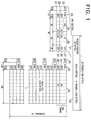
- Fig. 1 is a schematic diagram showing a sector format of an optical disc according to an embodiment of the present invention.
- data is encoded corresponding to the 4-9 modulation technique, which is the RLL (Run Length Limited) modulation technique.
- the 4-9 modulation technique is used to convert 4-bit data into a 9-bit signal pattern.
- the details of the 4-9 modulation technique are described in for example Japanese Patent Application No. 5-76692.
- one sector is composed of 42 frames.
- the first frame of the sector is a header portion 21 that is composed of 33 bytes.
- the rest (41 frames) of the sector other than the first frame is a data portion 22 that is composed of 1353 bytes.
- One optical disc has a plurality of successive sectors.
- the header portion 21 is composed of a 2-byte (DCC (23) + SYNC (24)), a 4-byte AM (Address Mark) (25), a 4-byte ID (26), a 2-byte first CRC (27), a 0.5-byte DCC (28), an 8-byte SLD (center Link Data)-1 (29), a 2-byte second CRC (30), a 0.5-byte DCC (31), an 8-byte SLD-2 (32), and a 2-byte third CRC (33).
- the 2-byte (DCC (23) + SYNC (24)) is a first synchronous pattern.
- the 4-byte AM (25) is a second synchronous pattern.
- the 4-byte ID (26) is an address information containing a sector number.
- the DCCs (23, 28, 31) are cancel codes that are added so as to suppress DC components of signals that have been converted corresponding to the NRZI technique.
- the SYNC (24) is a synchronous code that is used to generate a timing at which data is extracted, byte by byte, when data is demodulated.
- the frame synchronous signal which is composed of the DCC (23) and the SYNC (24), does not correspond to the 4-9 modulation technique.
- the frame synchronous signal contains a signal pattern that is not present in the 4-9 modulation code.
- the AM (25), which is the second synchronous pattern, is data that represents the position of the ID (26) and the delimitation of a sector.
- the AM (25) is also composed of a signal pattern that is not present in the 4-9 modulation code.
- the ID (26) is data that represents a sector number, which is address data.
- the first CRC (27) is an error check code for the ID (26).
- the SLD-1 (29) and SLD-2 (32) are data that represents data type (for example, image signal, character data, and so forth) of the sectors, subordinate relation of sectors, and so forth.
- the second CRC (30) is an error check code for the SLD-1 (29).
- the third CRC (33) is an error check code for the SLD-2 (32).
- Each (data portion 22) of the second to 42nd frames of the sectors is composed of a 2-byte frame synchronous signal (DCC (41) + SYNC (42)), 10-byte user data (43), a 0.5-byte DCC (44), 10-byte user data (45), a 0.5-byte DCC (46), and 10-byte user data (47).
- DCC 2-byte frame synchronous signal
- SYNC SYNC
- the frame synchronous signal (DCC (41) + SYNC (42)) is composed of a signal pattern that is not present in the 4-9 modulation code.
- the user data (43, 45, 47) contains an ECC (Error Correction Code).
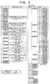
- Fig. 2 is a schematic diagram showing the construction of a code conversion table for the 4-9 modulation system.
- D n is a value of which an input binary data sequence is divided by every four bits and represented in hexadecimal (HEX) notation.
- HEX hexadecimal
- the minimum code inversion length (Tmin) and the maximum code inversion length (Tmax) in the 4-9 modulation code are 4T and 18T, respectively.
- Fig. 3 is a schematic diagram showing binary data of the frame synchronous signal (DCC + SYNC) and a signal pattern in which the binary data has been converted corresponding to the NRZI technique.
- Fig. 4 is a schematic diagram showing binary data of the AM (25) and a signal pattern in which the binary data has been converted corresponding to the NRZI technique.
- the AM (25) is converted corresponding to the NRZI technique, as shown in Fig. 4, 14 sequences of a code inversion length for 4T are followed by a sequence of a code inversion length for 8T, followed by a code inversion length for 8T or more in which 4T is the minimum code inversion length (Tmin) of the 4-9 modulation code.
- Tmin minimum code inversion length
- the signal pattern in which 14 sequences of a code inversion length for 4T take place is not present in the 4-9 modulation code. Since the 4-9 modulation code is not present in the signal pattern that represents the AM (25) and the signal pattern contains 14 sequences of a code inversion length for 4T, the AM (25) can be uniquely distinguished from other signal patterns and thereby easily and accurately detected.
- Fig. 5 is a schematic diagram showing a data arrangement in the case that an ECC (Error Correction Code) has been added to user data.
- ECC Error Correction Code
- six sectors compose one ECC group in which there are two error correction codes C1 and C2 as product codes.
- the C1 error correction code is generated and the error correcting process thereof is performed with a row of 90 bytes in the X (horizontal) direction of Fig. 5.
- the C2 error correction code is generated and the error correcting process thereof is preformed with a sequence of 84 bytes in the Z (diagonal) direction of Fig. 5.
- the SYNC and the DCC in the sector format shown in Fig. 1 are not included in the generating and error correcting range of the error correction codes C1 and C2.
- the AM (25), the ID (26), the first CRC (27), the SLD-1 (29), the second CRC (30), the SLD-2 (32), and the third CRC (33) of the header portion 21 are included in the generating and error correcting range of the generation of the error correction codes C1 and C2.
- the AM (25) is composed of a special signal pattern that does not correspond to the modulation rule, it cannot be included in the calculating range of the error correction codes C1 and C2. Thus, before the error correction codes C1 and C2 are generated and calculated on the recording apparatus side, the AM (25) is substituted with fixed data corresponding to the modulation rule. Thereafter, the error correction codes C1 and C2 are generated for the AM (25).
- all the user data other than the DCC and the SYNC are included in the generating range of the error correction codes C1 and C2 and the error correcting process.
- Fig. 6 is a block diagram showing the construction of the recording apparatus.
- the recording apparatus comprises a memory 61, a fixed data generating circuit 62, a first selecting circuit 63, a parity generating circuit 64, a 4-9 modulating circuit 65, a formatting circuit 66, an AM generating circuit 67, a second selecting circuit 68, and an NRZI modulating circuit 69.
- the operation of the recording apparatus will be described.
- Data to be recorded on an optical disc is stored in the memory 61.
- the data stored in the memory 61 is user data such as image data, and sound data, ID, CRC, and SLD.
- Data is read from the memory 61 corresponding to the error correction codes C1 and C2 of the parity generating circuit 64.
- the data is supplied to the parity generating circuit 64 through the first selecting circuit 63.
- the first selecting circuit 63 selects 4-byte fixed data (such as "00", “00", “00”, "00"" from the fixed data generating circuit 62 and supplies the fixed data to the parity generating circuit 64.
- the parity generating circuit 64 calculates the error correction codes C1 and C2, adds them to the record data, and supplies the resultant data to the 4-9 modulating circuit 65.
- the 4-9 modulating circuit 65 converts the input data sequence into a 4-9 modulation code and supplies the 4-9 modulation code to the formatting circuit 66.
- the formatting circuit 66 adds a predetermined signal pattern of the SYNC and the DCC to a data sequence of the 4-9 modulated data so as to form sector data composed of sectors.
- the formatting circuit 66 supplies the sector data to the NRZI modulating circuit 69.
- the NRZI modulating circuit 69 performs the NRZI modulation for the sector data.
- the second selecting circuit 68 selects the predetermined signal pattern shown in Fig. 4 from the AM generating circuit 67 and supplies the signal pattern to the NRZI modulating circuit 69.
- a record processing portion (not shown) records the NRZI-modulated sector data on the optical disc.
- Fig. 7 is a block diagram showing the construction of the reproducing apparatus.
- the reproducing apparatus comprises a SYNC detecting circuit 71, a frame synchronizing circuit 72, an AM detecting circuit 73, a sector synchronizing circuit 74, a timing circuit 75, a 4-9 demodulating circuit 76, a selecting circuit 77, a fixed data generating circuit 78, a memory 79, an error correcting circuit 80, and a CRC checking circuit 81.
- a reproduction processing portion (not shown) reads a signal from an optical disc and supplies the signal to the SYNC detecting circuit 71 and the AM detecting circuit 73.
- the SYNC detecting circuit 71 detects a SYNC pattern from the input disc reproduced signal. Thereafter, the frame synchronous circuit 72 synchronizes with frames corresponding to the SYNC detected signal received from the SYNC detecting circuit 71. At this point, synchronous protection is performed so that out-of-synchronism does not takes place even if a few SYNCs are lost.
- the AM detecting circuit 73 extracts an AM pattern whenever every 42 SYNCs take place.
- the sector synchronizing circuit 74 synchronizes with sectors corresponding to the AM detected signal received from the AM detecting circuit 73. At this point, as with the frame synchronizing circuit 72, the sector synchronizing circuit 74 protects synchronism of sectors so as to prevent out-of-synchronism of sectors from taking place even if the AM pattern is lost.
- the timing circuit 75 receives the synchronous signals from the frame synchronizing circuit 72 and the sector synchronizing circuit 74, generates a demodulating timing signal and a write address signal, and supplies the demodulating timing signal to the 4-9 demodulating circuit 76 and the write address signal to the memory 79.
- the selecting circuit 77 selects fixed data received from the fixed data generating circuit 78 and supplies the fixed data to the memory 79.
- the fixed data is the same as the fixed data generated by the fixed data generating circuit 62 of the recording apparatus. In other words, the fixed data is for example "00", “00", "00", "00".
- the error correcting circuit 80 corrects errors of ID (26), CRC (27), SLD-1 (29), CRC (30), SLD-2 (32), and CRC (33) of the header portion 21 as well as the user data. Even if an error takes place in these portions, when it is in the error correctable range, it can be corrected to correct data.
- the 4-9 modulated data is supplied to the CRC checking circuit 81 that detects errors of ID (26), SLD-1 (29), and SLD-2 (32) of the header portion 21 without need to perform the error correcting process.
- the detected result of the CRC checking circuit 81 is supplied to a control circuit.
- the control circuit performs a predetermined control process corresponding to a situation.
- the error correcting process is performed.
- the CRC checking circuit 81 is activated so as to detect an error of the header portion 21 and perform control process for the header portion 21.
- a signal can be recorded on a recording medium in a sector format where an error of sector identification data may be corrected and the detecting accuracy of the identification data is high when data is reproduced.
- the second synchronous pattern may be substituted with a predetermined signal pattern that is present in a signal pattern of user data and that is included in the generating and calculating range of the error correction codes so as to suppress the remainder.
- sectors can be composed with a multiple of the period of frames.
- an error sector identification data may be corrected.
- an error of the identification data can be detected corresponding to the error detected data.
- an error of the identification data may be detected without need to perform the error correcting process. Thereafter, the identification data is used for the control process.
Landscapes
- Engineering & Computer Science (AREA)
- Signal Processing (AREA)
- Signal Processing For Digital Recording And Reproducing (AREA)
- Optical Recording Or Reproduction (AREA)
Applications Claiming Priority (4)
| Application Number | Priority Date | Filing Date | Title |
|---|---|---|---|
| JP6046007A JP2920065B2 (ja) | 1994-03-16 | 1994-03-16 | データ記録方法、記録装置、再生装置及び再生方法 |
| JP46007/94 | 1994-03-16 | ||
| JP4600794 | 1994-03-16 | ||
| EP94120910A EP0673029A1 (de) | 1994-03-16 | 1994-12-29 | Aufzeichnungsträger, Signalaufzeichnungsgerät dafür Signalwiedergabegerät dafür |
Related Parent Applications (2)
| Application Number | Title | Priority Date | Filing Date |
|---|---|---|---|
| EP94120910A Division EP0673029A1 (de) | 1994-03-16 | 1994-12-29 | Aufzeichnungsträger, Signalaufzeichnungsgerät dafür Signalwiedergabegerät dafür |
| EP94120910.8 Division | 1994-12-29 |
Publications (3)
| Publication Number | Publication Date |
|---|---|
| EP0802536A2 true EP0802536A2 (de) | 1997-10-22 |
| EP0802536A3 EP0802536A3 (de) | 1997-11-12 |
| EP0802536B1 EP0802536B1 (de) | 2000-09-20 |
Family
ID=12735018
Family Applications (2)
| Application Number | Title | Priority Date | Filing Date |
|---|---|---|---|
| EP94120910A Ceased EP0673029A1 (de) | 1994-03-16 | 1994-12-29 | Aufzeichnungsträger, Signalaufzeichnungsgerät dafür Signalwiedergabegerät dafür |
| EP97106997A Expired - Lifetime EP0802536B1 (de) | 1994-03-16 | 1994-12-29 | Aufzeichnungsträger, Signalaufzeichnungsgerät und Signalwiedergabegerät dafür |
Family Applications Before (1)
| Application Number | Title | Priority Date | Filing Date |
|---|---|---|---|
| EP94120910A Ceased EP0673029A1 (de) | 1994-03-16 | 1994-12-29 | Aufzeichnungsträger, Signalaufzeichnungsgerät dafür Signalwiedergabegerät dafür |
Country Status (5)
| Country | Link |
|---|---|
| US (4) | US5666338A (de) |
| EP (2) | EP0673029A1 (de) |
| JP (1) | JP2920065B2 (de) |
| KR (1) | KR0172143B1 (de) |
| DE (1) | DE69425985T2 (de) |
Cited By (1)
| Publication number | Priority date | Publication date | Assignee | Title |
|---|---|---|---|---|
| WO2004053870A1 (en) * | 2002-12-10 | 2004-06-24 | Samsung Electronics Co., Ltd. | Information storage medium and method of recording/reproducing the same |
Families Citing this family (22)
| Publication number | Priority date | Publication date | Assignee | Title |
|---|---|---|---|---|
| JPH07254230A (ja) * | 1994-03-16 | 1995-10-03 | Toshiba Corp | 記録媒体及び記録媒体への信号記録方法 |
| JP2882302B2 (ja) * | 1995-02-24 | 1999-04-12 | 株式会社日立製作所 | 情報の記録方法及び再生方法 |
| WO1996031881A1 (en) * | 1995-04-03 | 1996-10-10 | Matsushita Electric Industrial Co., Ltd. | Recording medium, data transmission method and apparatus, and data reproduction method and apparatus |
| CA2192062C (en) * | 1995-04-04 | 2002-10-29 | Shin-Ichi Tanaka | Recording medium, recording method and apparatus, and reproduction method and apparatus |
| JP3457093B2 (ja) * | 1995-04-14 | 2003-10-14 | 松下電器産業株式会社 | 記録媒体並びにデジタル変復調方法およびその装置 |
| JPH0982039A (ja) * | 1995-09-18 | 1997-03-28 | Sony Corp | 情報記録方法および追記型光ディスク記録方法 |
| JP3394127B2 (ja) * | 1995-12-05 | 2003-04-07 | 株式会社東芝 | ディジタルデータの伝送方法 |
| EP1022736B1 (de) | 1996-02-08 | 2002-07-03 | Matsushita Electric Industrial Co., Ltd. | Optische Platte, optische Plattenvorrichtung, und Verfahren zur Wiedergabe von Informationen auf der optischen Platte |
| JP3103505B2 (ja) * | 1996-06-26 | 2000-10-30 | 三菱電機株式会社 | 光ディスク及び光ディスク駆動装置 |
| JP3729362B2 (ja) * | 1996-07-15 | 2005-12-21 | ソニー株式会社 | 記録媒体再生装置および記録媒体再生方法 |
| JP3433021B2 (ja) * | 1996-09-20 | 2003-08-04 | パイオニア株式会社 | Pll回路 |
| JPH10312650A (ja) * | 1997-05-14 | 1998-11-24 | Ricoh Co Ltd | 光ディスク記録装置 |
| JP4099914B2 (ja) * | 1999-12-10 | 2008-06-11 | ソニー株式会社 | 光ディスク及び光ディスク装置 |
| US7239592B2 (en) * | 2000-04-03 | 2007-07-03 | Stmicroelectronics S.A. | Method for indicating a sector on a data medium and data medium suited to this method |
| US6990058B1 (en) * | 2000-04-03 | 2006-01-24 | Dphi Acquisitions, Inc. | Structure and method for storing data on optical disks |
| JP4263340B2 (ja) * | 2000-07-07 | 2009-05-13 | ヒタチグローバルストレージテクノロジーズネザーランドビーブイ | 回転記憶装置およびその制御方法 |
| EP1317755A1 (de) * | 2000-09-05 | 2003-06-11 | Koninklijke Philips Electronics N.V. | Informationsträger, vorrichtung zum abrufen von informationen vom informationsträger und vorrichtung zum aufzeichnen von informationen auf dem informationsträger |
| JP4348851B2 (ja) * | 2000-09-21 | 2009-10-21 | ソニー株式会社 | 記録媒体、ディスク記録装置および方法、並びにディスク再生装置及び方法 |
| JP2003069535A (ja) * | 2001-06-15 | 2003-03-07 | Mitsubishi Electric Corp | 誤り訂正多重化装置、誤り訂正多重分離装置、これらを用いた光伝送システムおよび誤り訂正多重化伝送方法 |
| JP2003085898A (ja) * | 2001-09-12 | 2003-03-20 | Toshiba Corp | 情報記憶媒体、情報記録装置、情報記録方法、情報再生装置、及び情報再生装置 |
| JP4020021B2 (ja) * | 2003-05-30 | 2007-12-12 | ヤマハ株式会社 | 光ディスク装置 |
| US7570555B2 (en) * | 2004-01-09 | 2009-08-04 | Panasonic Corporation | Digital data demodulator |
Family Cites Families (21)
| Publication number | Priority date | Publication date | Assignee | Title |
|---|---|---|---|---|
| US4544962A (en) * | 1981-07-06 | 1985-10-01 | Matsushita Electric Industrial Co., Ltd. | Method and apparatus for processing binary data |
| JPS58220211A (ja) * | 1982-06-16 | 1983-12-21 | Matsushita Electric Ind Co Ltd | デイジタル変調方法 |
| US4791622A (en) * | 1983-09-19 | 1988-12-13 | Storage Technology Partners 11 | Optical data format employing resynchronizable data sectors |
| JPS62234426A (ja) * | 1986-04-04 | 1987-10-14 | Sony Corp | エラ−訂正方法 |
| DE3780517T2 (de) * | 1986-05-31 | 1993-03-25 | Sony Corp | Methoden und geraet zum suchen einer zieladresse auf einem aufzeichnungsmedium. |
| US4907215A (en) * | 1986-08-27 | 1990-03-06 | Sony Corporation | Integral optical recording of product code in data areas |
| JP2526875B2 (ja) * | 1986-11-05 | 1996-08-21 | ソニー株式会社 | デイジタル情報記録装置 |
| US4998252A (en) * | 1987-08-06 | 1991-03-05 | Sony Corporation | Method and apparatus for transmitting digital data |
| JP2645025B2 (ja) * | 1987-09-04 | 1997-08-25 | 株式会社日立製作所 | 光記録再生方法 |
| JP2829963B2 (ja) * | 1988-05-16 | 1998-12-02 | ソニー株式会社 | ディジタルデータ記録/再生装置 |
| JP2586621B2 (ja) * | 1988-12-16 | 1997-03-05 | 松下電器産業株式会社 | データ記録方法 |
| JP2534778B2 (ja) * | 1989-09-26 | 1996-09-18 | 株式会社日立製作所 | 情報記録/再生方式および情報記録/再生装置 |
| JPH03119574A (ja) * | 1989-10-02 | 1991-05-21 | Sony Corp | 記録情報発生方法 |
| JPH0652630A (ja) * | 1991-03-28 | 1994-02-25 | Sony Corp | データ記録方法 |
| JP3256981B2 (ja) * | 1991-04-05 | 2002-02-18 | ソニー株式会社 | データ記録方法 |
| EP0517478B1 (de) * | 1991-06-04 | 1998-08-12 | Quantum Corporation | Servodatenrückgewinnungsschaltung für Plattenspeicher mit digitalen eingelassenen Servosektoren |
| JP3318841B2 (ja) * | 1992-08-20 | 2002-08-26 | ソニー株式会社 | 再生装置および再生方法 |
| JPH06338141A (ja) * | 1993-03-29 | 1994-12-06 | Nippon Hoso Kyokai <Nhk> | 追記型記録媒体、フォーマット装置および方法、データ読みだし装置および方法、ならびにデータ書き込み装置および方法 |
| JPH0730431A (ja) * | 1993-04-02 | 1995-01-31 | Toshiba Corp | データ変復調方式および変復調装置 |
| US5623467A (en) * | 1993-09-27 | 1997-04-22 | Matsushita Electric Industrial Co., Ltd. | Data recording apparatus for recording data in sector units |
| JP2786810B2 (ja) * | 1994-03-16 | 1998-08-13 | 株式会社東芝 | 光ディスクおよびその信号記録装置ならびに信号再生装置 |
-
1994
- 1994-03-16 JP JP6046007A patent/JP2920065B2/ja not_active Expired - Lifetime
- 1994-12-23 US US08/363,320 patent/US5666338A/en not_active Expired - Lifetime
- 1994-12-29 EP EP94120910A patent/EP0673029A1/de not_active Ceased
- 1994-12-29 DE DE69425985T patent/DE69425985T2/de not_active Expired - Lifetime
- 1994-12-29 EP EP97106997A patent/EP0802536B1/de not_active Expired - Lifetime
-
1995
- 1995-03-16 KR KR1019950005422A patent/KR0172143B1/ko not_active Expired - Lifetime
-
1997
- 1997-03-04 US US08/812,947 patent/US5848051A/en not_active Expired - Lifetime
- 1997-04-29 US US08/848,177 patent/US5956306A/en not_active Expired - Lifetime
- 1997-04-29 US US08/848,176 patent/US5909417A/en not_active Expired - Lifetime
Cited By (4)
| Publication number | Priority date | Publication date | Assignee | Title |
|---|---|---|---|---|
| WO2004053870A1 (en) * | 2002-12-10 | 2004-06-24 | Samsung Electronics Co., Ltd. | Information storage medium and method of recording/reproducing the same |
| RU2321083C2 (ru) * | 2002-12-10 | 2008-03-27 | Самсунг Электроникс Ко., Лтд. | Информационная запоминающая среда и устройство записи и/или воспроизведения для использования с информационной запоминающей средой |
| CN100547667C (zh) * | 2002-12-10 | 2009-10-07 | 三星电子株式会社 | 信息存储介质和记录/再现其的方法 |
| RU2396609C2 (ru) * | 2002-12-10 | 2010-08-10 | Самсунг Электроникс Ко., Лтд. | Способ записи информации на информационную запоминающую среду и/или воспроизведения информации с этой среды |
Also Published As
| Publication number | Publication date |
|---|---|
| JP2920065B2 (ja) | 1999-07-19 |
| US5848051A (en) | 1998-12-08 |
| KR0172143B1 (ko) | 1999-04-15 |
| EP0673029A1 (de) | 1995-09-20 |
| KR950027677A (ko) | 1995-10-18 |
| US5666338A (en) | 1997-09-09 |
| US5909417A (en) | 1999-06-01 |
| DE69425985D1 (de) | 2000-10-26 |
| JPH07254239A (ja) | 1995-10-03 |
| EP0802536B1 (de) | 2000-09-20 |
| EP0802536A3 (de) | 1997-11-12 |
| US5956306A (en) | 1999-09-21 |
| DE69425985T2 (de) | 2001-04-26 |
Similar Documents
| Publication | Publication Date | Title |
|---|---|---|
| EP0802536B1 (de) | Aufzeichnungsträger, Signalaufzeichnungsgerät und Signalwiedergabegerät dafür | |
| EP0673028B1 (de) | Aufzeichnungsmedium, Signalaufzeichnungsgerät dazu, und Signalwiedergabegerät dazu | |
| USRE42962E1 (en) | Optical disk and method and apparatus for recording and then playing information back from that disk | |
| EP1403869B1 (de) | Vorrichtung und Verfahren zur Bildung eines Signals | |
| JPH02301074A (ja) | 信号転送装置 | |
| MXPA96006099A (en) | Method of digital data transmission | |
| JPH10501916A (ja) | 記録媒体、記録方法と装置及び再生方法と装置 | |
| US7017101B2 (en) | Information storage medium, information recording method and information processing method | |
| JPH0562363A (ja) | 記録再生方法 | |
| JP2868744B2 (ja) | データ記録方法、記録装置、再生装置及び再生方法 | |
| US5175655A (en) | Method and apparatus for verifying a signal recorded in an encoded form on a medium | |
| US5684784A (en) | CAV recording/ reproducing apparatus for dividing input data in an amount proportional if the radial lengths of a plurality of recording areas | |
| JP3708619B2 (ja) | 消失フラグを用いたエラー訂正システム | |
| JPH02131625A (ja) | 誤り訂正装置 | |
| EP0673027A2 (de) | Aufzeichnungsmedium und Verfahren zur Aufzeichnung eines Signals darauf | |
| JPH0991885A (ja) | 同期情報付加方法及び同期情報付加装置、並びに同期情報検出方法及び同期情報検出装置 | |
| JPS628369A (ja) | デ−タ読取方式 | |
| JPH09265736A (ja) | 情報処理装置 | |
| JP2005129222A (ja) | 記録坦体及びそのような記録坦体を読み取る装置 | |
| JPH08147888A (ja) | ディジタル信号記録方法及び装置 | |
| JPH04232663A (ja) | データ復号装置 | |
| JPH0519783B2 (de) | ||
| JPH02156479A (ja) | メモリ装置の記憶再生方式 | |
| JPH06120844A (ja) | 誤り信号訂正装置 | |
| HK1063685B (en) | Signal forming apparatus and method |
Legal Events
| Date | Code | Title | Description |
|---|---|---|---|
| PUAI | Public reference made under article 153(3) epc to a published international application that has entered the european phase |
Free format text: ORIGINAL CODE: 0009012 |
|
| PUAL | Search report despatched |
Free format text: ORIGINAL CODE: 0009013 |
|
| 17P | Request for examination filed |
Effective date: 19970523 |
|
| AC | Divisional application: reference to earlier application |
Ref document number: 673029 Country of ref document: EP |
|
| AK | Designated contracting states |
Kind code of ref document: A2 Designated state(s): DE FR GB |
|
| AK | Designated contracting states |
Kind code of ref document: A3 Designated state(s): DE FR GB NL |
|
| 17Q | First examination report despatched |
Effective date: 19980202 |
|
| GRAG | Despatch of communication of intention to grant |
Free format text: ORIGINAL CODE: EPIDOS AGRA |
|
| GRAG | Despatch of communication of intention to grant |
Free format text: ORIGINAL CODE: EPIDOS AGRA |
|
| GRAG | Despatch of communication of intention to grant |
Free format text: ORIGINAL CODE: EPIDOS AGRA |
|
| GRAH | Despatch of communication of intention to grant a patent |
Free format text: ORIGINAL CODE: EPIDOS IGRA |
|
| RBV | Designated contracting states (corrected) |
Designated state(s): DE FR GB |
|
| GRAH | Despatch of communication of intention to grant a patent |
Free format text: ORIGINAL CODE: EPIDOS IGRA |
|
| GRAA | (expected) grant |
Free format text: ORIGINAL CODE: 0009210 |
|
| AC | Divisional application: reference to earlier application |
Ref document number: 673029 Country of ref document: EP |
|
| AK | Designated contracting states |
Kind code of ref document: B1 Designated state(s): DE FR GB |
|
| REF | Corresponds to: |
Ref document number: 69425985 Country of ref document: DE Date of ref document: 20001026 |
|
| ET | Fr: translation filed | ||
| PLBE | No opposition filed within time limit |
Free format text: ORIGINAL CODE: 0009261 |
|
| STAA | Information on the status of an ep patent application or granted ep patent |
Free format text: STATUS: NO OPPOSITION FILED WITHIN TIME LIMIT |
|
| 26N | No opposition filed | ||
| REG | Reference to a national code |
Ref country code: GB Ref legal event code: IF02 |
|
| PGFP | Annual fee paid to national office [announced via postgrant information from national office to epo] |
Ref country code: DE Payment date: 20131224 Year of fee payment: 20 Ref country code: GB Payment date: 20131227 Year of fee payment: 20 |
|
| PGFP | Annual fee paid to national office [announced via postgrant information from national office to epo] |
Ref country code: FR Payment date: 20131209 Year of fee payment: 20 |
|
| REG | Reference to a national code |
Ref country code: DE Ref legal event code: R071 Ref document number: 69425985 Country of ref document: DE |
|
| REG | Reference to a national code |
Ref country code: DE Ref legal event code: R071 Ref document number: 69425985 Country of ref document: DE |
|
| REG | Reference to a national code |
Ref country code: GB Ref legal event code: PE20 Expiry date: 20141228 |
|
| PG25 | Lapsed in a contracting state [announced via postgrant information from national office to epo] |
Ref country code: GB Free format text: LAPSE BECAUSE OF EXPIRATION OF PROTECTION Effective date: 20141228 |