EP0787836B1 - Method for preparing silicon melt from polycrystalline silicon charge - Google Patents
Method for preparing silicon melt from polycrystalline silicon charge Download PDFInfo
- Publication number
- EP0787836B1 EP0787836B1 EP96308146A EP96308146A EP0787836B1 EP 0787836 B1 EP0787836 B1 EP 0787836B1 EP 96308146 A EP96308146 A EP 96308146A EP 96308146 A EP96308146 A EP 96308146A EP 0787836 B1 EP0787836 B1 EP 0787836B1
- Authority
- EP
- European Patent Office
- Prior art keywords
- polycrystalline silicon
- crucible
- granular
- chunk
- silicon
- Prior art date
- Legal status (The legal status is an assumption and is not a legal conclusion. Google has not performed a legal analysis and makes no representation as to the accuracy of the status listed.)
- Expired - Lifetime
Links
- 229910021420 polycrystalline silicon Inorganic materials 0.000 title claims description 183
- XUIMIQQOPSSXEZ-UHFFFAOYSA-N Silicon Chemical compound [Si] XUIMIQQOPSSXEZ-UHFFFAOYSA-N 0.000 title claims description 32
- 229910052710 silicon Inorganic materials 0.000 title claims description 32
- 239000010703 silicon Substances 0.000 title claims description 32
- 238000000034 method Methods 0.000 title claims description 21
- 238000011068 loading method Methods 0.000 claims description 25
- 238000002844 melting Methods 0.000 claims description 13
- 230000008018 melting Effects 0.000 claims description 13
- 229910021421 monocrystalline silicon Inorganic materials 0.000 claims description 13
- 238000004519 manufacturing process Methods 0.000 claims description 10
- 238000010926 purge Methods 0.000 claims description 9
- 238000010438 heat treatment Methods 0.000 claims description 8
- 238000001816 cooling Methods 0.000 claims description 6
- 230000000694 effects Effects 0.000 claims description 5
- HJELPJZFDFLHEY-UHFFFAOYSA-N silicide(1-) Chemical compound [Si-] HJELPJZFDFLHEY-UHFFFAOYSA-N 0.000 claims 14
- 239000013078 crystal Substances 0.000 description 13
- 239000000155 melt Substances 0.000 description 10
- 238000005245 sintering Methods 0.000 description 9
- 239000007789 gas Substances 0.000 description 7
- 230000007547 defect Effects 0.000 description 6
- LIVNPJMFVYWSIS-UHFFFAOYSA-N silicon monoxide Chemical compound [Si-]#[O+] LIVNPJMFVYWSIS-UHFFFAOYSA-N 0.000 description 6
- 239000008187 granular material Substances 0.000 description 5
- 239000000463 material Substances 0.000 description 5
- 230000008646 thermal stress Effects 0.000 description 5
- 238000012856 packing Methods 0.000 description 4
- XKRFYHLGVUSROY-UHFFFAOYSA-N Argon Chemical compound [Ar] XKRFYHLGVUSROY-UHFFFAOYSA-N 0.000 description 2
- UFHFLCQGNIYNRP-UHFFFAOYSA-N Hydrogen Chemical compound [H][H] UFHFLCQGNIYNRP-UHFFFAOYSA-N 0.000 description 2
- 238000002109 crystal growth method Methods 0.000 description 2
- 238000004090 dissolution Methods 0.000 description 2
- 238000007667 floating Methods 0.000 description 2
- 230000004927 fusion Effects 0.000 description 2
- 239000001257 hydrogen Substances 0.000 description 2
- 229910052739 hydrogen Inorganic materials 0.000 description 2
- 239000012535 impurity Substances 0.000 description 2
- 239000011261 inert gas Substances 0.000 description 2
- NJPPVKZQTLUDBO-UHFFFAOYSA-N novaluron Chemical compound C1=C(Cl)C(OC(F)(F)C(OC(F)(F)F)F)=CC=C1NC(=O)NC(=O)C1=C(F)C=CC=C1F NJPPVKZQTLUDBO-UHFFFAOYSA-N 0.000 description 2
- 239000002245 particle Substances 0.000 description 2
- 238000002360 preparation method Methods 0.000 description 2
- 239000010453 quartz Substances 0.000 description 2
- VYPSYNLAJGMNEJ-UHFFFAOYSA-N silicon dioxide Inorganic materials O=[Si]=O VYPSYNLAJGMNEJ-UHFFFAOYSA-N 0.000 description 2
- 229910052786 argon Inorganic materials 0.000 description 1
- 238000006243 chemical reaction Methods 0.000 description 1
- 230000003247 decreasing effect Effects 0.000 description 1
- 238000013461 design Methods 0.000 description 1
- 238000004031 devitrification Methods 0.000 description 1
- 238000007598 dipping method Methods 0.000 description 1
- 238000005516 engineering process Methods 0.000 description 1
- 239000010410 layer Substances 0.000 description 1
- 238000010309 melting process Methods 0.000 description 1
- 238000004377 microelectronic Methods 0.000 description 1
- 238000013021 overheating Methods 0.000 description 1
- 238000007790 scraping Methods 0.000 description 1
- 239000004065 semiconductor Substances 0.000 description 1
- 238000010561 standard procedure Methods 0.000 description 1
- 230000035882 stress Effects 0.000 description 1
- 230000000153 supplemental effect Effects 0.000 description 1
- 239000002344 surface layer Substances 0.000 description 1
Images


Classifications
-
- C—CHEMISTRY; METALLURGY
- C30—CRYSTAL GROWTH
- C30B—SINGLE-CRYSTAL GROWTH; UNIDIRECTIONAL SOLIDIFICATION OF EUTECTIC MATERIAL OR UNIDIRECTIONAL DEMIXING OF EUTECTOID MATERIAL; REFINING BY ZONE-MELTING OF MATERIAL; PRODUCTION OF A HOMOGENEOUS POLYCRYSTALLINE MATERIAL WITH DEFINED STRUCTURE; SINGLE CRYSTALS OR HOMOGENEOUS POLYCRYSTALLINE MATERIAL WITH DEFINED STRUCTURE; AFTER-TREATMENT OF SINGLE CRYSTALS OR A HOMOGENEOUS POLYCRYSTALLINE MATERIAL WITH DEFINED STRUCTURE; APPARATUS THEREFOR
- C30B15/00—Single-crystal growth by pulling from a melt, e.g. Czochralski method
- C30B15/02—Single-crystal growth by pulling from a melt, e.g. Czochralski method adding crystallising materials or reactants forming it in situ to the melt
-
- C—CHEMISTRY; METALLURGY
- C30—CRYSTAL GROWTH
- C30B—SINGLE-CRYSTAL GROWTH; UNIDIRECTIONAL SOLIDIFICATION OF EUTECTIC MATERIAL OR UNIDIRECTIONAL DEMIXING OF EUTECTOID MATERIAL; REFINING BY ZONE-MELTING OF MATERIAL; PRODUCTION OF A HOMOGENEOUS POLYCRYSTALLINE MATERIAL WITH DEFINED STRUCTURE; SINGLE CRYSTALS OR HOMOGENEOUS POLYCRYSTALLINE MATERIAL WITH DEFINED STRUCTURE; AFTER-TREATMENT OF SINGLE CRYSTALS OR A HOMOGENEOUS POLYCRYSTALLINE MATERIAL WITH DEFINED STRUCTURE; APPARATUS THEREFOR
- C30B15/00—Single-crystal growth by pulling from a melt, e.g. Czochralski method
-
- C—CHEMISTRY; METALLURGY
- C30—CRYSTAL GROWTH
- C30B—SINGLE-CRYSTAL GROWTH; UNIDIRECTIONAL SOLIDIFICATION OF EUTECTIC MATERIAL OR UNIDIRECTIONAL DEMIXING OF EUTECTOID MATERIAL; REFINING BY ZONE-MELTING OF MATERIAL; PRODUCTION OF A HOMOGENEOUS POLYCRYSTALLINE MATERIAL WITH DEFINED STRUCTURE; SINGLE CRYSTALS OR HOMOGENEOUS POLYCRYSTALLINE MATERIAL WITH DEFINED STRUCTURE; AFTER-TREATMENT OF SINGLE CRYSTALS OR A HOMOGENEOUS POLYCRYSTALLINE MATERIAL WITH DEFINED STRUCTURE; APPARATUS THEREFOR
- C30B29/00—Single crystals or homogeneous polycrystalline material with defined structure characterised by the material or by their shape
- C30B29/02—Elements
Definitions
- the present invention generally relates to the production of single crystal silicon, and specifically, to a process for preparing a molten silicon melt from polycrystalline silicon.
- the invention particularly relates, in a preferred embodiment, to a process for preparing a molten silicon melt from a mixed charge of chunk and granular polycrystalline silicon.
- CZ Czochralski
- the polycrystalline silicon melted to form the molten silicon is typically irregularly shaped chunk polycrystalline silicon prepared by the Siemens process or, alternatively, free-flowing, generally spherically-shaped granular polycrystalline silicon, typically prepared by a relatively simpler and more efficient fluidized-bed reaction process.
- Granular polycrystalline silicon is typically about 1-5 mm in diameter, and generally has a packing density which is about 20% higher than chunk polycrystalline silicon. The preparation and characteristics of chunk and granular polycrystalline silicon are further detailed in F. Shimura, Semiconductor Silicon Crystal Technology , pages 116-121, Academic Press (San Diego CA, 1989) and the references cited therein.
- CZ crucibles are typically initially charged entirely with chunk polycrystalline silicon.
- loadings cause problems in the subsequent manufacture of the silicon crystal ingot.
- the edges of the chunks under the load of a full charge can scratch and gouge the crucible wall, particularly at the bottom of the crucible, resulting in a damaged crucible and in particles of crucible floating on or being suspended in the silicon melt.
- impurities significantly increase the likelihood of dislocations forming within the single crystal, and decrease the dislocation-free single crystal production yields and throughput.
- the chunk polycrystalline silicon charge can shift or the lower portion of the chunk-polycrystalline silicon can melt away and leave either a "hanger” of unmelted material stuck to the crucible wall above the melt or a "bridge” of unmelted material bridging between opposing sides of the crucible wall over the melt.
- the charge shifts or a hanger or bridge collapses, it may splatter molten silicon and/or cause mechanical stress damage to the crucible.
- initial loadings of 100% chunk-polycrystalline silicon limits the volume of material which can be charged due to the poor packing densities of such chunk materials. The volume limitations directly impact single crystal throughput.
- granular polycrystalline silicon offers advantages over chunk polycrystalline silicon with respect to preparation and packing density, the full capacity charging of granular polycrystalline silicon into the crucible and the melting thereof can also introduce undesirable impurities and defects into the single crystal silicon ingot.
- granular polycrystalline silicon has primarily been used for the supplemental recharging of an existing silicon melt, as exemplified in U.S. Patent No.'s 5,242,531 and 5,242,667 to Klingshirn et al. and Koziol et al., respectively.
- Patent Abstracts of Japan, Vol. 013, No. 408 (C-634), 8 September 1989 and JP-A-01/148779 disclose a Czochralski crystal growth method comprising loading of polycrystalline silicon into a crucible on top of a solidified surface layer which covers a silicon melt.
- the present invention is directed to a process for preparing a silicon melt from polycrystalline silicon for use in producing single crystal silicon by the Czochralski method.
- the process comprises loading granular polycrystalline and chunk polycrystalline silicon into a crucible with the chunk polycrystalline silicon being loaded onto the granular polycrystalline silicon.
- the granular polycrystalline silicon and the chunk polycrystalline silicon are then melted to form a silicon melt.
- granular polycrystalline silicon and chunk polycrystalline silicon are loaded into a crucible having a centerline and an inner surface which includes a bottom and a wall.
- the wall has an upper portion which includes about 50% of the surface area of the wall.
- the granular polycrystalline silicon is loaded onto the bottom, and, after loading, the granular polycrystalline silicon does not contact the upper portion of the wall.
- the height of the granular polycrystalline silicon at or near the centerline of the crucible is greater than its height at or near the wall.
- the chunk polycrystalline silicon is loaded onto the granular polycrystalline silicon.
- the polycrystalline silicon is heated and a substantial portion of the granular polycrystalline silicon is melted before a substantial portion of the chunk polycrystalline silicon is melted. While heating, the granular and chunk polycrystalline silicon are exposed to a purge gas and the chunk polycrystalline silicon thermally shields the granular polycrystalline silicon from cooling effects of the purge gas. Any unmelted granular polycrystalline silicon and chunk polycrystalline silicon are melted to form a silicon melt.
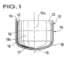
- FIG. 1 is a section view of an empty Czochralski crucible.
- FIGS. 2(a) through 2(f) are section views showing alternative embodiments of a mixed initial charge of granular and chunk polycrystalline silicon.
- FIGS. 3(a) through 3(c) are section views showing various stages of melting an initial mixed charge of granular and chunk polycrystalline silicon.
- granular polycrystalline silicon is loaded into a Czochralski crucible with chunk polycrystalline silicon as a mixed charge, and arranged in a manner which minimizes sintering or fusion of granules of polycrystalline silicon to other granules or to the crucible wall during subsequent melting.
- Such sintering or fusion problems occur when silicon melts are prepared from a crucible packed to its maximum capacity entirely with granular polycrystalline silicon.
- Aggregates formed by granule-to-granule sintering have mirrored surfaces which reflect radiant heat back to the crucible wall, thereby resulting in excessive and non-uniform heating thereof.
- the weight of sintered aggregates adhering to the crucible wall can deform the wall and further affect the rotational uniform thermal symmetry. Moreover, large amounts of power are required to melt the sintered aggregates, and significant overheating of the crucible occurs and induces additional thermal stresses. Such thermal stresses further contribute to deformation of the crucible and also cause non-uniform dissolution of the crucible into the melt such that particles of the crucible become loosened and suspended in the melt, resulting in reduced zero-defect crystal production yields and throughput.
- Crucible deformation can cause excessive generation of silicon monoxide, thereby further reducing zero-defect yields.
- the degree of thermal stress on the crucible generally increases with the size of initial granular polycrystalline silicon loading.
- the present invention substantially reduces the melting difficulties which arise when a silicon melt is prepared with a full capacity initial charge of 100% granular polycrystalline silicon.
- granular polycrystalline silicon is loaded into an empty, unheated crucible and arranged such that, after loading, it does not contact the upper portion of the crucible wall. Chunk polycrystalline silicon is loaded onto the granular polycrystalline silicon. As the crucible is heated, the weight of the chunk polycrystalline silicon exerts a downward force which keeps the granular polycrystalline silicon near the hottest region of the crucible. The chunk polycrystalline silicon also thermally shields the granular polycrystalline silicon from the cooling effects of a purge gas.
- a silicon melt may be prepared as described herein with less mechanical and thermal stress on the crucible, thereby minimizing deformation of the crucible, dissolution of the crucible into the melt and generation of silicon monoxide.
- the mixed charge loadings of the present invention overcome the volume limitations associated with initial charges of 100% chunk polycrystalline silicon.
- higher capacity silicon melts prepared according to the present invention may be used for producing single crystal silicon ingots with fewer defects at a higher throughput.
- FIG 1 illustrates one type of crucible 10 suitable for preparing silicon melts according to the present invention.
- the crucible 10 should be of a material such as quartz which is compatible with preparing single crystal silicon ingots by the Czochralski method.
- the crucible 10 has an inner surface 12, an outer surface 14, a centerline 15 and a top edge 16.
- the inner surface 12 of the crucible 10 may be coated with a devitrification promoter.
- the inner surface 12 includes a bottom portion 17, a corner portion 18 and a side or wall portion 19, referred to hereinafter as the bottom 17, corner 18 and wall 19, respectively.
- the wall 19 is substantially vertical and the bottom 17 is substantially horizontal.
- the wall 19 defines a substantially vertical circumferential area which includes a top portion 19(a) and a bottom portion 19(b), the top and bottom portions 19(a), 19(b) each including about 50% of the total surface area of the wall 19.
- the approximate division between the top and bottom portions 19(a), 19(b) is generally illustrated by phantom line 21.
- the bottom 17 is parabolic, having a slope with a substantially greater horizontal component than vertical component.
- the corner 18 is a curved annular boundary region in the vicinity of the intersection of the wall 19 and bottom 17. The corner 18 intersects the wall 19 where the curvature of the corner 18 ceases, illustrated generally as line 22.
- the corner 18 has a radius of curvature which is less than the radius of curvature of the bottom 17 and generally intersects the bottom 17 where the radius of curvature changes.
- the centerline 15 of the crucible 10 is substantially parallel to the wall 19 and intersects a geometric centerpoint of the bottom 17. While the geometry of the illustrated crucible 10 is preferred, the particular geometry of the crucible 10 may vary from the illustrated embodiment and still fall within the scope of the invention.
- both granular polycrystalline silicon 1 and chunk polycrystalline silicon 2 are loaded into a crucible 10 to prepare a mixed charge.
- the crucible 10 preferably contains no molten silicon when the polycrystalline silicon 1, 2 is loaded into it.
- the crucible 10 is preferably empty and at ambient temperature prior to loading. However, if the crucible 10 is being recharged after a previous crystal-pulling run, then the crucible 10 may contain some residual molten silicon or some resolidified residual silicon, and may be at an elevated temperature when loaded.
- the granular polycrystalline silicon 1 preferably contains less than about 600 ppma hydrogen and most preferably less than about 20 ppma hydrogen. Standard chunk polycrystalline silicon 2 may be used.
- the granular polycrystalline silicon 1 is preferably loaded onto the bottom 17 of the crucible 10.
- the granular polycrystalline silicon 1 may also cover the corner 18 (Figs. 2(c) and 3(a)), and the lower portion 19(b) of the walls 19 of the inner surface 12 of the crucible 10 (Figs. 2(b), 2(d) and 2(e)).
- the granular polycrystalline silicon 1 is preferably loaded such that, after loading, none of the granular polycrystalline silicon 1 is in contact with the upper portion 19(a) of the wall 19.
- Granular polycrystalline silicon 1 contact with the lower portion 19(b) is preferably minimized, but some contact therewith may be necessary to achieve the desired proportion of granular polycrystalline silicon 1 in the mixed charge.
- the granular polycrystalline silicon 1 may, in an alternative arrangement illustrated in Figure 2(f), be loaded over a layer of chunk polycrystalline silicon 2 which had been previously loaded over the bottom 17. In such a situation, some of the granular polycrystalline silicon 1 will, due to its small size, fall through the crevices between chunks 2 and also cover a portion of the bottom 17.
- the granular polycrystalline silicon 1 is preferably loaded as a mound with the peak of the mound being closer to the centerline 15 than to the wall 19. That is, the granular polycrystalline silicon 1 is preferably loaded to a height at or near the centerline 15 of the crucible 10 which is greater than its height at the wall 19 of the crucible 10. Such mounding maximizes the total charge while minimizing the degree of contact between the granular polycrystalline silicon 1 and the upper portion of the wall 19(a).
- the chunk polycrystalline silicon 2 is loaded onto the granular polycrystalline silicon 1, and preferably, completely overlies the granular polycrystalline silicon 1. As discussed in detail below, such a configuration allows the chunk polycrystalline silicon 2 to exert a downward force on the granular polycrystalline silicon 1 and to shield the underlying granular polycrystalline silicon 1 from cooling effects associated with a purge gas.
- the chunk polycrystalline silicon is preferably loaded such that, after loading, it contacts at least the upper portion 19(a) of the wall 19. Most preferably, chunk polycrystalline silicon 2 rather than granular polycrystalline silicon 1 contacts the both the upper and lower portions 19(a), 19(b) of the wall 19.
- the chunk polycrystalline silicon 2 should be loaded in a manner which minimizes gouging or scraping of the walls 19 of the inner surface 12.
- the exact profile of the interface 20 between the granular polycrystalline silicon 1 and the chunk polycrystalline silicon 2 is not narrowly critical. As shown in Figures 2(a) through 2(c), the slope of the sides of the mounded pile of granular polycrystalline silicon 1 may vary in steepness, with the maximum slope being defined by the angle of repose for the particular granular polycrystalline silicon 1, typically about 30 degrees. Moreover, the profile of the interface 20 between the granular and chunk polycrystalline silicon 1, 2 may be flat (Fig. 2(c)) or even slightly lower at the centerline 15 of the crucible 10 as compared to near the walls 19 (Fig. 2(d)). It is similarly not narrowly critical that the chunk polycrystalline silicon 2 completely overlie or cover the granular polycrystalline silicon 1. As shown in Figure 2(e), a portion of the granular polycrystalline silicon 1 may be uncovered.
- the amount of granular polycrystalline silicon 1 loaded into the crucible 10 to form a mixed charge preferably ranges from about 5% to about 80% and more preferably from about 10% to about 75% by weight of the total polycrystalline silicon 1, 2 loaded into the crucible 10.
- the amount of granular polycrystalline silicon 1 most preferably ranges from about 15% to about 50% by weight of the total mixed charge.
- the preferred proportionate amount of granular polycrystalline silicon 1 in the mixed charge generally increases as crucible size increases, since the change in the size of the bottom 17 of a larger sized crucible 10 as compared to a smaller sized crucible 10, is proportionately larger than the corresponding change in size of crucible walls 19.
- the granular polycrystalline silicon 1 loaded preferably comprises from about 15% to about 25% of the total mixed charge loading, whereas in larger sized crucibles, the amount of granular polycrystalline silicon 1 preferably ranges up to about 50%, by weight, of the total mixed charge.
- the total mixed charge loading is generally greater than the full capacity loading obtainable with 100% chunk polycrystalline silicon 2 for the same size crucible 10.
- a typical 18 inch (45 cm) crucible can be loaded with a total mixed charge of about 70 kg, which represents a 10 kg (about 17%) increase over the typical 60 kg maximum-capacity loading achieved with 100% chunk polycrystalline silicon.
- Such higher mixed-charge capacities result from the increased packing density of granular polycrystalline silicon 1, and therefore, the use of higher proportions of granular polycrystalline silicon 1 in the mixed charge generally result in a capacity advantage over loadings of pure chunk polycrystalline silicon 2.
- the crucible 10 is placed in a conventional CZ silicon crystal growth apparatus and the granular and chunk polycrystalline silicon 1, 2 are melted to form a silicon melt 3.
- the polycrystalline silicon 1 situated near the bottom 17 of the crucible 10 is preferably heated and melted before the chunk polycrystalline silicon 2 situated higher in the crucible 10.
- a substantial portion of the granular polycrystalline silicon 1 is melted before a substantial portion of the chunk polycrystalline silicon 2 is melted.
- the relative proportions may vary based on crucible design, heating profile, and the size and type of crystal grower, about 50% of the granular polycrystalline silicon 1 is preferably melted before about 50% of the chunk polycrystalline silicon 2 is melted, and most preferably before about 25% of the chunk polycrystalline silicon 2 is melted.
- the crucible 10 is supported by a susceptor 31 which is situated on a movable pedestal 32.
- the pedestal 32 is positioned such that the bottom of the crucible 10 is near the top of the heater 30 (Fig. 3(a)) and gradually lowered into the space inside the heater 30 (Figs. 3(b) and 3(c)).
- the speed at which the crucible 10 is lowered into closer proximity of the heater 30 and the value of other factors affecting melting of the polycrystalline silicon, such as heater power, crucible rotation and system pressure, may be the same as is employed for melting loadings of pure chunk polycrystalline silicon 2. (Example 1).
- the weight of the chunk polycrystalline silicon 2 overlying the granular polycrystalline silicon 1 exerts a downward force on any unmelted granular polycrystalline silicon 1.
- the downward force exerted by the chunk polycrystalline silicon 2 helps to keep the granular polycrystalline silicon 1 away from the crucible walls 19 and near the lower region of the crucible 10. That is, the weight of the chunk polycrystalline silicon 2 helps preclude the unmelted granular polycrystalline silicon 1 from floating away from the lower region of the crucible 10, which is generally relatively hotter due to the heating arrangement described above.
- the granular and chunk polycrystalline silicon 1, 2 are typically exposed, while heating, to a purge gas 35 to flush out undesirable gasses such as SiO(g).
- the purge gas 35 is typically an inert gas such as argon and typically flows at a rate ranging from about 10 l/min to about 300 l/min, depending on the type and size of the crystal puller.
- the granular and chunk polycrystalline silicon 1, 2 are preferably arranged such that the chunk polycrystalline silicon 2 thermally shields the granular polycrystalline silicon 1 from the cooling effects of the purge gas 35.
- the chunk polycrystalline silicon 2 overlying the granular polycrystalline silicon 1 acts as such a thermal shield.
- Granule-to-granule and granule-to-wall sintering is minimized by several facets of the present invention.
- Granule-to-wall sintering is minimized in the upper portion 19(a) of the wall 19 by arranging the granular polycrystalline silicon 1 so as not to be in contact therewith.
- the chunk polycrystalline silicon 2 exerts a downward force on and thermally shields the underlying granular polycrystalline silicon 1, thereby keeping the granular polycrystalline silicon 1 in the hottest region of the crucible 10 and minimizing cooling thereof, respectively.
- heating the crucible 10 from the bottom upwards so as to melt a substantial portion of the granular polycrystalline silicon 1 before melting a substantial portion of the chunk polycrystalline silicon 2 also contributes to minimize sintering. As shown in Figure 3(c), the heating is continued to melt any unmelted granular polycrystalline silicon 1 and chunk polycrystalline silicon 2, thereby forming a silicon melt 3.
- a 75 kg mixed charge consisting of 60 kg chunk polycrystalline silicon and 15 kg granular polycrystalline silicon was loaded into an 18 inch (45 cm) quartz crucible according to the preferred embodiment of the present invention, as described above.
- the mixed charge was melted in a Leybold CZ crystal puller.
- the crucible was positioned such that the top edge of the crucible was about 13 cm above the top of the heater and the bottom of the crucible was about 24 cm below the top of the heater.
- the crucible was then lowered into the space between the heater at an average speed of about 1.2 mm/min. While lowering, the heater power level was step-wise varied as follows: 92 kw for 10 minutes; 115 kw for 30 minutes; and 125 kw for 85 minutes. The lowering continued until the crucible was at a position where the top edge of the crucible was about 2 cm below the top of the heater.
- the crucible was held at this position for 100 minutes with the power maintained at 112 kw.
- the crucible was then raised to a position where the top edge of the crucible was 1 cm below the top of the heater and held at this position for 15 minutes with the power at 108 kw.
- the crucible was then raised to a position where the top edge of the crucible was at the same level as the top of the heater and held at this position at a power level of 100 kw until the polycrystalline silicon became completely molten.
- the system pressure was 10 mbar (1000 Pa)
- the crucible was rotated at a speed of 2 rpm
- the polycrystalline silicon was purged with an inert gas at a flow rate of 30 l/min.
- Molten silicon melts prepared from 100% chunk polycrystalline silicon loadings and from mixed charge loadings of the present invention were used to produce single crystal silicon ingots by the Czochralski method. Data was collected to determine the length of zero defect (ZD) single-crystal silicon for each of the silicon melts prepared.
- ZD zero defect
Landscapes
- Chemical & Material Sciences (AREA)
- Engineering & Computer Science (AREA)
- Crystallography & Structural Chemistry (AREA)
- Materials Engineering (AREA)
- Metallurgy (AREA)
- Organic Chemistry (AREA)
- Crystals, And After-Treatments Of Crystals (AREA)
- Silicon Compounds (AREA)
Applications Claiming Priority (2)
| Application Number | Priority Date | Filing Date | Title |
|---|---|---|---|
| US08/595,075 US5814148A (en) | 1996-02-01 | 1996-02-01 | Method for preparing molten silicon melt from polycrystalline silicon charge |
| US595075 | 1996-02-01 |
Publications (3)
| Publication Number | Publication Date |
|---|---|
| EP0787836A2 EP0787836A2 (en) | 1997-08-06 |
| EP0787836A3 EP0787836A3 (en) | 1998-04-01 |
| EP0787836B1 true EP0787836B1 (en) | 2001-01-17 |
Family
ID=24381626
Family Applications (1)
| Application Number | Title | Priority Date | Filing Date |
|---|---|---|---|
| EP96308146A Expired - Lifetime EP0787836B1 (en) | 1996-02-01 | 1996-11-12 | Method for preparing silicon melt from polycrystalline silicon charge |
Country Status (8)
| Country | Link |
|---|---|
| US (1) | US5814148A (enExample) |
| EP (1) | EP0787836B1 (enExample) |
| JP (1) | JPH09328391A (enExample) |
| KR (1) | KR970062081A (enExample) |
| CN (1) | CN1157342A (enExample) |
| DE (1) | DE69611597T2 (enExample) |
| MY (1) | MY112066A (enExample) |
| SG (1) | SG76498A1 (enExample) |
Families Citing this family (27)
| Publication number | Priority date | Publication date | Assignee | Title |
|---|---|---|---|---|
| EP0856599A3 (en) * | 1997-01-31 | 2000-03-22 | Komatsu Electronic Metals Co., Ltd | Apparatus for feeding raw material into a quartz crucible and method of feeding the same |
| JP3189764B2 (ja) * | 1997-09-29 | 2001-07-16 | 住友金属工業株式会社 | シリコン単結晶原料の溶解方法 |
| US5919303A (en) * | 1997-10-16 | 1999-07-06 | Memc Electronic Materials, Inc. | Process for preparing a silicon melt from a polysilicon charge |
| US6589332B1 (en) | 1998-11-03 | 2003-07-08 | Memc Electronic Materials, Inc. | Method and system for measuring polycrystalline chunk size and distribution in the charge of a Czochralski process |
| US6284040B1 (en) | 1999-01-13 | 2001-09-04 | Memc Electronic Materials, Inc. | Process of stacking and melting polycrystalline silicon for high quality single crystal production |
| US6344083B1 (en) | 2000-02-14 | 2002-02-05 | Memc Electronic Materials, Inc. | Process for producing a silicon melt |
| US6749683B2 (en) | 2000-02-14 | 2004-06-15 | Memc Electronic Materials, Inc. | Process for producing a silicon melt |
| US8021483B2 (en) * | 2002-02-20 | 2011-09-20 | Hemlock Semiconductor Corporation | Flowable chips and methods for the preparation and use of same, and apparatus for use in the methods |
| US7141114B2 (en) * | 2004-06-30 | 2006-11-28 | Rec Silicon Inc | Process for producing a crystalline silicon ingot |
| NO324710B1 (no) * | 2004-12-29 | 2007-12-03 | Elkem Solar As | Fremgangsmate for fylling av digel med silisium av solcellekvalitet |
| JP4961753B2 (ja) * | 2006-01-20 | 2012-06-27 | 株式会社Sumco | 単結晶製造管理システム及び方法 |
| JP4753308B2 (ja) * | 2006-07-13 | 2011-08-24 | Sumco Techxiv株式会社 | 半導体ウェーハ素材の溶解方法及び半導体ウェーハの結晶育成方法 |
| CN101148777B (zh) * | 2007-07-19 | 2011-03-23 | 任丙彦 | 直拉法生长掺镓硅单晶的方法和装置 |
| US20090120353A1 (en) * | 2007-11-13 | 2009-05-14 | Memc Electronic Materials, Inc. | Reduction of air pockets in silicon crystals by avoiding the introduction of nearly-insoluble gases into the melt |
| US20100107966A1 (en) * | 2008-11-05 | 2010-05-06 | Memc Electronic Materials, Inc. | Methods for preparing a melt of silicon powder for silicon crystal growth |
| JP5511945B2 (ja) * | 2009-04-29 | 2014-06-04 | シリコー マテリアルズ インコーポレイテッド | Umg−si材料精製のためのプロセス管理 |
| JP2012140285A (ja) * | 2010-12-28 | 2012-07-26 | Siltronic Japan Corp | シリコン単結晶インゴットの製造方法 |
| US20120260845A1 (en) * | 2011-04-14 | 2012-10-18 | Rec Silicon Inc | Polysilicon system |
| CN102953117B (zh) * | 2011-08-31 | 2015-06-10 | 上海普罗新能源有限公司 | 硅锭的铸造方法 |
| CN102732945B (zh) * | 2012-04-13 | 2015-11-25 | 英利能源(中国)有限公司 | 一种单晶硅铸锭装料方法 |
| WO2014037965A1 (en) * | 2012-09-05 | 2014-03-13 | MEMC ELECTRONIC METERIALS S.p.A. | Method of loading a charge of polysilicon into a crucible |
| CN103074681B (zh) * | 2013-02-17 | 2016-03-16 | 英利集团有限公司 | 一种二次加料方法 |
| CN107604446A (zh) * | 2017-10-25 | 2018-01-19 | 宁晋晶兴电子材料有限公司 | 一种新型的熔融表皮料结构及其熔融方法 |
| DE102019208670A1 (de) * | 2019-06-14 | 2020-12-17 | Siltronic Ag | Verfahren zur Herstellung von Halbleiterscheiben aus Silizium |
| CN114086243A (zh) * | 2021-11-29 | 2022-02-25 | 曲靖晶龙电子材料有限公司 | 单晶硅棒的制备方法 |
| CN115467013A (zh) * | 2022-08-22 | 2022-12-13 | 包头美科硅能源有限公司 | 一种用于拉晶生产中提高颗粒硅投料量的方法 |
| CN115404356B (zh) * | 2022-09-22 | 2024-03-22 | 同创普润(上海)机电高科技有限公司 | 一种降低高纯铝熔体中不熔物含量的方法 |
Family Cites Families (14)
| Publication number | Priority date | Publication date | Assignee | Title |
|---|---|---|---|---|
| US4249988A (en) * | 1978-03-15 | 1981-02-10 | Western Electric Company, Inc. | Growing crystals from a melt by controlling additions of material thereto |
| WO1986006764A1 (en) * | 1985-05-17 | 1986-11-20 | J.C. Schumacher Company | Continuously pulled single crystal silicon ingots |
| JPS6287489A (ja) * | 1985-10-12 | 1987-04-21 | Sumitomo Electric Ind Ltd | るつぼの回収方法及び装置 |
| JPH01148779A (ja) * | 1987-12-03 | 1989-06-12 | Toshiba Ceramics Co Ltd | 結晶成分の供給方法 |
| JPH01286995A (ja) * | 1988-05-12 | 1989-11-17 | Toshiba Ceramics Co Ltd | シリコン単結晶の製造方法 |
| JPH03193694A (ja) * | 1989-12-21 | 1991-08-23 | Sumitomo Metal Ind Ltd | 結晶成長装置 |
| JPH03199189A (ja) * | 1989-12-27 | 1991-08-30 | Kawasaki Steel Corp | 半導体単結晶の製造方法 |
| DE4106589C2 (de) | 1991-03-01 | 1997-04-24 | Wacker Siltronic Halbleitermat | Kontinuierliches Nachchargierverfahren mit flüssigem Silicium beim Tiegelziehen nach Czochralski |
| US5242667A (en) | 1991-07-26 | 1993-09-07 | Ferrofluidics Corporation | Solid pellet feeder for controlled melt replenishment in continuous crystal growing process |
| JPH05139886A (ja) * | 1991-11-21 | 1993-06-08 | Toshiba Corp | 砒素化合物単結晶の製造方法 |
| JP2506525B2 (ja) * | 1992-01-30 | 1996-06-12 | 信越半導体株式会社 | シリコン単結晶の製造方法 |
| JP2531415B2 (ja) * | 1992-03-24 | 1996-09-04 | 住友金属工業株式会社 | 結晶成長方法 |
| JPH05319978A (ja) * | 1992-05-22 | 1993-12-03 | Sumitomo Metal Ind Ltd | 溶融層法による単結晶引き上げ方法 |
| US5588993A (en) * | 1995-07-25 | 1996-12-31 | Memc Electronic Materials, Inc. | Method for preparing molten silicon melt from polycrystalline silicon charge |
-
1996
- 1996-02-01 US US08/595,075 patent/US5814148A/en not_active Expired - Lifetime
- 1996-10-30 MY MYPI96004510A patent/MY112066A/en unknown
- 1996-11-12 EP EP96308146A patent/EP0787836B1/en not_active Expired - Lifetime
- 1996-11-12 DE DE69611597T patent/DE69611597T2/de not_active Expired - Fee Related
- 1996-11-29 KR KR1019960059989A patent/KR970062081A/ko not_active Ceased
- 1996-12-25 CN CN96117958A patent/CN1157342A/zh active Pending
-
1997
- 1997-01-31 JP JP9018503A patent/JPH09328391A/ja active Pending
- 1997-02-01 SG SG1997000229A patent/SG76498A1/en unknown
Also Published As
| Publication number | Publication date |
|---|---|
| JPH09328391A (ja) | 1997-12-22 |
| MY112066A (en) | 2001-03-31 |
| EP0787836A3 (en) | 1998-04-01 |
| KR970062081A (ko) | 1997-09-12 |
| US5814148A (en) | 1998-09-29 |
| DE69611597D1 (de) | 2001-02-22 |
| SG76498A1 (en) | 2000-11-21 |
| DE69611597T2 (de) | 2001-05-31 |
| EP0787836A2 (en) | 1997-08-06 |
| CN1157342A (zh) | 1997-08-20 |
Similar Documents
| Publication | Publication Date | Title |
|---|---|---|
| EP0787836B1 (en) | Method for preparing silicon melt from polycrystalline silicon charge | |
| KR100506288B1 (ko) | 다결정 실리콘 충전물로부터 실리콘 용융체를 제조하는 공정 | |
| EP0756024B1 (en) | Method for preparing molten silicon melt from polycrystalline silicon charge | |
| CA1261715A (en) | Apparatus and process for growing monocrystals of semiconductor materials from shallow crucibles by czochralski technique | |
| EP1151154B1 (en) | Process of stacking and melting polycrystalline silicon for high quality single crystal production | |
| US20100107966A1 (en) | Methods for preparing a melt of silicon powder for silicon crystal growth | |
| EP1446517B1 (en) | Intermittent feeding technique for increasing the melting rate of polycrystalline silicon | |
| JPH09328391A5 (enExample) | ||
| KR100331552B1 (ko) | 잉곳-용융물 경계의 중앙 및 가장자리에서의 온도구배의 조절에 의한 단결정 실리콘 잉곳의 제조를 위한 초크랄스키 풀러, 상기 초크랄스키 풀러용 열차단체 및 상기 초크랄스키 풀러의 개량방법. | |
| JPS6117798B2 (enExample) | ||
| JP2531415B2 (ja) | 結晶成長方法 | |
| JP4120777B2 (ja) | InP単結晶の製造方法及びInP単結晶 | |
| EP0892091A1 (en) | Graphite support vessels having a low concentration of calcium impurities and use thereof for production of single-crystal silicon | |
| JP2990661B2 (ja) | 単結晶成長方法 | |
| JPH11217290A (ja) | 石英ガラスルツボ | |
| JP2700145B2 (ja) | 化合物半導体単結晶の製造方法 | |
| KR19990008776A (ko) | 저농도의 칼슘 불순물을 갖는 흑연지지 용기 및 단결정 실리콘의 생산에 그 용기를 이용하는 공정 | |
| JPH03131592A (ja) | 結晶成長装置 | |
| JPH01188500A (ja) | 化合物半導体単結晶の製造方法 |
Legal Events
| Date | Code | Title | Description |
|---|---|---|---|
| PUAI | Public reference made under article 153(3) epc to a published international application that has entered the european phase |
Free format text: ORIGINAL CODE: 0009012 |
|
| AK | Designated contracting states |
Kind code of ref document: A2 Designated state(s): DE FR GB IT |
|
| PUAL | Search report despatched |
Free format text: ORIGINAL CODE: 0009013 |
|
| AK | Designated contracting states |
Kind code of ref document: A3 Designated state(s): DE FR GB IT |
|
| 17P | Request for examination filed |
Effective date: 19980911 |
|
| 17Q | First examination report despatched |
Effective date: 19990505 |
|
| GRAG | Despatch of communication of intention to grant |
Free format text: ORIGINAL CODE: EPIDOS AGRA |
|
| GRAG | Despatch of communication of intention to grant |
Free format text: ORIGINAL CODE: EPIDOS AGRA |
|
| GRAH | Despatch of communication of intention to grant a patent |
Free format text: ORIGINAL CODE: EPIDOS IGRA |
|
| GRAH | Despatch of communication of intention to grant a patent |
Free format text: ORIGINAL CODE: EPIDOS IGRA |
|
| GRAA | (expected) grant |
Free format text: ORIGINAL CODE: 0009210 |
|
| AK | Designated contracting states |
Kind code of ref document: B1 Designated state(s): DE FR GB IT |
|
| REF | Corresponds to: |
Ref document number: 69611597 Country of ref document: DE Date of ref document: 20010222 |
|
| ET | Fr: translation filed | ||
| ITF | It: translation for a ep patent filed | ||
| PLBE | No opposition filed within time limit |
Free format text: ORIGINAL CODE: 0009261 |
|
| STAA | Information on the status of an ep patent application or granted ep patent |
Free format text: STATUS: NO OPPOSITION FILED WITHIN TIME LIMIT |
|
| REG | Reference to a national code |
Ref country code: GB Ref legal event code: IF02 |
|
| 26N | No opposition filed | ||
| PGFP | Annual fee paid to national office [announced via postgrant information from national office to epo] |
Ref country code: FR Payment date: 20031110 Year of fee payment: 8 |
|
| PGFP | Annual fee paid to national office [announced via postgrant information from national office to epo] |
Ref country code: GB Payment date: 20031112 Year of fee payment: 8 |
|
| PGFP | Annual fee paid to national office [announced via postgrant information from national office to epo] |
Ref country code: DE Payment date: 20031120 Year of fee payment: 8 |
|
| PG25 | Lapsed in a contracting state [announced via postgrant information from national office to epo] |
Ref country code: GB Free format text: LAPSE BECAUSE OF NON-PAYMENT OF DUE FEES Effective date: 20041112 |
|
| PG25 | Lapsed in a contracting state [announced via postgrant information from national office to epo] |
Ref country code: DE Free format text: LAPSE BECAUSE OF NON-PAYMENT OF DUE FEES Effective date: 20050601 |
|
| GBPC | Gb: european patent ceased through non-payment of renewal fee |
Effective date: 20041112 |
|
| PG25 | Lapsed in a contracting state [announced via postgrant information from national office to epo] |
Ref country code: FR Free format text: LAPSE BECAUSE OF NON-PAYMENT OF DUE FEES Effective date: 20050729 |
|
| REG | Reference to a national code |
Ref country code: FR Ref legal event code: ST |
|
| PG25 | Lapsed in a contracting state [announced via postgrant information from national office to epo] |
Ref country code: IT Free format text: LAPSE BECAUSE OF NON-PAYMENT OF DUE FEES;WARNING: LAPSES OF ITALIAN PATENTS WITH EFFECTIVE DATE BEFORE 2007 MAY HAVE OCCURRED AT ANY TIME BEFORE 2007. THE CORRECT EFFECTIVE DATE MAY BE DIFFERENT FROM THE ONE RECORDED. Effective date: 20051112 |