EP0778620B1 - Vertikales MOS-Halbleiterbauelement - Google Patents
Vertikales MOS-Halbleiterbauelement Download PDFInfo
- Publication number
- EP0778620B1 EP0778620B1 EP96119619A EP96119619A EP0778620B1 EP 0778620 B1 EP0778620 B1 EP 0778620B1 EP 96119619 A EP96119619 A EP 96119619A EP 96119619 A EP96119619 A EP 96119619A EP 0778620 B1 EP0778620 B1 EP 0778620B1
- Authority
- EP
- European Patent Office
- Prior art keywords
- current
- cell region
- semiconductor layer
- cell
- current sensing
- Prior art date
- Legal status (The legal status is an assumption and is not a legal conclusion. Google has not performed a legal analysis and makes no representation as to the accuracy of the status listed.)
- Expired - Lifetime
Links
- 239000004065 semiconductor Substances 0.000 title claims description 42
- 239000010410 layer Substances 0.000 description 19
- 230000003071 parasitic effect Effects 0.000 description 19
- 238000001514 detection method Methods 0.000 description 12
- 239000012535 impurity Substances 0.000 description 9
- 230000015556 catabolic process Effects 0.000 description 5
- 238000009792 diffusion process Methods 0.000 description 5
- 238000009413 insulation Methods 0.000 description 4
- 239000011229 interlayer Substances 0.000 description 4
- 230000001154 acute effect Effects 0.000 description 3
- 230000003247 decreasing effect Effects 0.000 description 3
- 230000005669 field effect Effects 0.000 description 3
- 230000003111 delayed effect Effects 0.000 description 1
- 230000001419 dependent effect Effects 0.000 description 1
- 230000004048 modification Effects 0.000 description 1
- 238000012986 modification Methods 0.000 description 1
- 229910052710 silicon Inorganic materials 0.000 description 1
- 239000010703 silicon Substances 0.000 description 1
- 239000000758 substrate Substances 0.000 description 1
Images


Classifications
-
- H—ELECTRICITY
- H01—ELECTRIC ELEMENTS
- H01L—SEMICONDUCTOR DEVICES NOT COVERED BY CLASS H10
- H01L27/00—Devices consisting of a plurality of semiconductor or other solid-state components formed in or on a common substrate
- H01L27/02—Devices consisting of a plurality of semiconductor or other solid-state components formed in or on a common substrate including semiconductor components specially adapted for rectifying, oscillating, amplifying or switching and having potential barriers; including integrated passive circuit elements having potential barriers
- H01L27/0203—Particular design considerations for integrated circuits
- H01L27/0248—Particular design considerations for integrated circuits for electrical or thermal protection, e.g. electrostatic discharge [ESD] protection
-
- H—ELECTRICITY
- H01—ELECTRIC ELEMENTS
- H01L—SEMICONDUCTOR DEVICES NOT COVERED BY CLASS H10
- H01L29/00—Semiconductor devices specially adapted for rectifying, amplifying, oscillating or switching and having potential barriers; Capacitors or resistors having potential barriers, e.g. a PN-junction depletion layer or carrier concentration layer; Details of semiconductor bodies or of electrodes thereof ; Multistep manufacturing processes therefor
- H01L29/66—Types of semiconductor device ; Multistep manufacturing processes therefor
- H01L29/68—Types of semiconductor device ; Multistep manufacturing processes therefor controllable by only the electric current supplied, or only the electric potential applied, to an electrode which does not carry the current to be rectified, amplified or switched
- H01L29/70—Bipolar devices
- H01L29/72—Transistor-type devices, i.e. able to continuously respond to applied control signals
- H01L29/739—Transistor-type devices, i.e. able to continuously respond to applied control signals controlled by field-effect, e.g. bipolar static induction transistors [BSIT]
- H01L29/7393—Insulated gate bipolar mode transistors, i.e. IGBT; IGT; COMFET
- H01L29/7395—Vertical transistors, e.g. vertical IGBT
Definitions
- the present invention relates to a vertical MOS type semiconductor device and, more particularly, to an IGBT (Insulated Gate Bipolar Transistor) with a current sensing function which is constituted of a plurality of principal current cells and at least one current sensing cell.
- IGBT Insulated Gate Bipolar Transistor
- an external resistor is connected between a principal electrode and a current sensing electrode.
- the IGBT generally senses a current by detecting a difference in potential between the electrodes.
- FIG. 1 illustrates the structure of the prior art IGBT having a current sensing function.
- a plurality of gate oxide films 102 are formed on one major surface of an N-type semiconductor layer 101, and a plurality of gate electrodes 103 are arranged on their respective gate oxide films 102.
- Each of P-type base regions 104 is formed between two gate electrodes 103 in the surface of the N-type semiconductor layer 101.
- Emitter regions 105 are provided in the surface portion of each of the P-type base regions 104.
- a P-type semiconductor layer 106 serving as a collector region is formed on the other major surface of the N-type semiconductor layer 101.
- Interlayer insulation films 107 are provided so as to cover the gate electrodes 103, and a principal electrode 108 and a current sensing electrode 109 are formed on the interlayer insulation films 107 and the one major surface of the N-type semiconductor substrate 101, thus completing a principal current cell region 110 and a current sensing cell region 111 arranged adjacent to each other.
- the width of the gate electrode 103 in each cell is constant, as is the interval between the gate electrodes 103.
- the channel of a MOS gate P-type base region 104 under the gate electrode 103
- the adjacent principal current cell region and current sensing cell region are connected to each other through an N drift region. Therefore, part of the current in the current sensing cell region 111, which is to flow through the external resistor (not shown), is caused to flow into the principal current cell region 110 through an internal parasitic resistor (resistive component RN - of the N-type semiconductor layer 101).
- the above parasitic resistor is a bulk resistor formed by silicon, it has its own temperature characteristics and increases in resistance as the temperature rises, thus causing a problem wherein the current flowing through the external resistor increases as the temperature rises and the detected voltage (difference in potential between external resistors) heightens.
- Rch indicates a resistive component of the channel.
- an IGBT having a structure capable of lessening the influence of temperature characteristics of the parasitic resistor is contrived.
- FIG. 2 illustrates an IGBT which is so constituted that the value of a parasitic resistor is larger than that of an external resistor in order to lessen the influence of temperature characteristics of the parasitic resistor.
- an interval a between adjacent P-type base regions 104 of the principal current cell 110 and current sensing cell 111 is greater than an interval b between other adjacent P-type base regions 104.
- the width of a gate electrode 103 between the cells 110 and 111 is set greater than that of another gate electrode 103 (an interval between adjacent gate electrodes 103 is fixed), and the width of an N drift region connecting the adjacent cells 110 and 111 is increased.
- the value of a parasitic resistor resistive component RN - of N-type semiconductor layer 101
- the temperature characteristics of the parasitic resistor are slightly improved. Since, moreover, the curvature of a depletion layer 101' is acute in an area of the layer 101' where the interval a between the P-type base regions 104 is increased, a breakdown voltage is lowered. (See B.J. Baliga, "Modern Power Device", pp.272 to pp.274, for example.)
- EP-A-669658 discloses the influence of a short protection circuit on the sensing function of an IGBT, especially during the turn-on period T ON of changing to the conductive state.
- a short protection circuit it is suggested to provide different first and second field effect type semiconductor elements so that a rise of the main current of said second field effect type semiconductor element is delayed from a rise of the main current of said first field effect type semiconductor element, if the device is turned on.
- Figure 16 of this document shows an IGBT having a main cell and a sense cell.
- the p base layers in the respective cells are different in that the diffusion depth of the used p-type impurity is different.
- the channel length in the sense cell is set to be longer than the length of the channel in the mail cell.
- the object of the present application is to provide an improved semiconductor device of a vertical MOS type, which prevents a breakdown voltage from being lowered, and prevents a detected voltage from increasing due to the internal parasitic resistance heightened by the rise of temperature, whereby the current detection precision is improved.
- the semiconductor device according to the present invention is so constituted that the on-voltage in the principal current cell is heightened at a higher rate than that in the current sensing cell. Even when the temperature of the device is increased, the current obtained from the current sensing cell can be fixed.
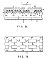
- FIGS. 3A and 3B illustrate an IGBT (Insulated Gate Bipolar Transistor) with a current sensing function according to a first embodiment of the present invention.
- FIG. 3A is a cross-sectional view of the main part of the IGBT, while FIG. 3B is a plan view of an arrangement pattern of base regions of the IGBT of FIG. 3A.
- a plurality of gate electrodes 13 are arranged on the major surface of an N-type semiconductor layer 11 with their respective gate oxide films 12 therebetween.
- P-type base regions 14a and 14b are each formed on the surface of the N-type semiconductor layer 11 and between adjacent gate electrodes 13, by double diffusion using the gate electrodes 13 as masks.
- An emitter region 15 is selectively provided in the surface area of each of the P-type base regions 14a and 14b.
- a P-type semiconductor layer 16 serving as a collector region is formed on the other major surface of the N-type semiconductor layer 11.
- An interlayer insulation film 17 is formed so as to cover each of the gate electrodes 13, and a principal electrode 18, which is connected to both the P-type base region 14a and emitter region 15, and a current sensing electrode 19, which is connected to both the P-type base region 14b and emitter region 15, are formed on the major surface of the N-type semiconductor layer 11 with the interlayer insulation film 17 interposed therebetween.
- the IGBT is thus constituted of a principal current cell region 21 and a current sensing cell region 22 adjacent to each other.
- the gate electrode (first gate electrode) 13 of a cell in the principal current cell region 21 and that (second gate electrode) 13 of a cell in the current sensing cell region 22 have the same width.
- the interval between the gate electrodes 13 of the cell in the principal current cell region 21 and that in the current sensing cell region 22 are different from each other. In other words, the latter interval is greater than the former.
- the widths of the respective P-type base regions 14a and 14b, which are to be formed using the gate electrodes 13 as masks, vary with the opening width of each of the masks, that is, the interval between the gate electrodes 13.
- the P-type base region 14b of the cell in the current detection cell region 22 is broader than the P-type base region 14a of the cell in the principal current cell region 21.
- the temperature characteristics of the parasitic resistor RN - slightly influences the current detection, but the influence can almost be eliminated.
- the temperature characteristic of on-voltage (potential difference in the vertical direction of the principal current cell) in the principal current cell region 21 and that of on-voltage (potential difference in the vertical direction of the current sensing cell) in the current sensing cell region 22 can be caused to differ from each other by varying in width from P-type base region 14a to P-type base region 14b.
- the resistive components of current flowing through the current sensing cell can be made larger than those in the principal current cell thereby to prevent the current from increasing in the current sensing cell due to the temperature characteristic of the parasitic resistor RN - . Consequently, even though the temperature of the IGBT increases, the fixed amount of current obtained from the current sensing cell can be maintained, and the precision of current detection can be improved between external resistors 31.
- the interval (L) between P-type base regions 14a and 14b is fixed for each cell (see FIG. 3B).
- the curvature of a depletion layer is not acute or the breakdown voltage is not lowered.
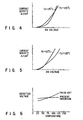
- FIG. 5 shows the relationship between the current density and the on-voltage in the current sensing cell. It is apparent from FIG. 5 that if the current sensing cell has the above constitution, its on-voltage increases at a higher rate than the on-voltage of the principal current cell at the high temperature. It is thus understood that the resistance of current flowing through the current sensing cell is easy to increase.
- the channel width of a MOS gate per unit area (an overlap of the P-type base region with the gate electrode) in the principal current cell is greater than that in the current sensing cell and accordingly, the base current to be supplied to the PNP transistor is increased, with the result that the on-voltage is prevented from increasing at a high rate even while the temperature is high and so is the current density.
- the influence of temperature characteristics of parasitic resistor RN - between the principal current cell and current sensing cell upon current detection can be eliminated by varying in structure from the former cell to the latter cell. More specifically, the temperature of the IGBT at which the on-voltage of the current sensing cell is zero is set higher than that at which the on-voltage of the principal current cell is zero.
- the increase rate of on-voltage in the current sensing cell is higher than that in the principal current cell. Since the decrease rate of current in the current sensing cell is higher when the temperature of the IGBT increases, the increase in current in the current sensing cell, which is caused by the temperature characteristic of parasitic resistor RN - , can be prevented.
- FIG. 6 shows the relationship between the detected voltage and the temperature in both the IGBT of the first embodiment and the prior art IGBT.
- an influence of temperature characteristic of parasitic resistor RN-between the principal current cell and current sensing cell upon current detection can be eliminated.
- the interval (L) between the P-type base regions is fixed for each of the cells.
- the principal current cell region 21 and current sensing cell region 22 differ from each other in interval between gate electrodes 13, the P-type base regions 14a and 14b are formed by double diffusion using the gate electrodes 13 as masks, and the P-type base region 14b in the current sensing cell region 22 is wider than the P-type base region 14a in the principal current cell region 21.
- the present invention is not limited to the constitution of the first embodiment. For example, even though the channel length of the cell in the current sensing cell region 22 is set greater than that in the principal current cell region 21, the same advantage can be expected.
- FIG. 7 illustrates an IGBT with a current sensing function not belonging to the present invention.
- the widths of gate electrodes 13 of cells both in a principal current cell region 21 and in a current sensing region 22 are the same, as is the interval between adjacent gate electrodes 13 in both the regions, whereas the cells vary in channel length from region 21 to region 22.
- the depths of P-type base regions 14a and 14b are the same.
- the channel length y of the cell of the current sensing cell region 22 is greater than the channel length x of the cell of the principal current cell region 21.
- the impurities are implanted in advance into that portion of an N-type semiconductor layer 11 where a long channel is to be formed before the gate electrode 13 is formed, and then diffused by double diffusion using the gate electrode 13 as a mask at the same time when the P-type base regions 14a and 14b are formed.
- the PNP transistor in the principal current cell region 21 becomes dominant, with the result that the on-voltage is prevented from increasing while the temperature of the IGBT and the density of the current are high.
- the value of parasitic resistor RN - becomes smaller as the channel length y increases, so that there is a fear of a slight influence upon current detection, but the precision of the current detection can be improved in substantially the same manner as in the first embodiment.
- FIG. 8 illustrates an IGBT with a current sensing function not belonging to the present invention.
- This IGBT is so constituted that P-type base regions 14a and 14b of the principal current cell region 21 and current sensing cell region 22 differ from each other in depth as well as in channel length. More specifically, the P-type base region 14b is expanded such that the channel length y of the cell thereof is greater than the channel length x of the cell of the P-type base region 14a.
- the P-type base regions 14a and 14b are formed separately, using the gate electrodes 13 as masks, by varying the impurities in amount.
- FIG. 9 illustrates an IGBT with a current sensing function according to a second embodiment of the present invention.
- the width of a gate electrode 13 formed between a principal current cell region 21 and a current sensing cell region 22 is greater than that of another gate electrode 13, while the intervals between adjacent gate electrodes 13 in the cell regions 21 and 22 are the same.
- a P-type base region 14b is extended to that portion of a drift region, connecting adjacent cells of the regions 21 and 22, which is formed directly under the gate electrode 13 and expanded by expanding the gate electrode 13.
- the channel length y of the cell of the current sensing cell region 22 is set longer than the channel length x of the cell of the principal current cell region 21, thereby fixing the interval between the P-type base regions 14a and 14b.
- the impurities are implanted in advance into that portion of an N-type semiconductor layer where a long channel is to be provided before the gate electrode 13 is formed, and then diffused by double diffusion using the gate electrode 13 as a mask at the same time when the P-type base regions 14a and 14b are formed. It is thus possible to maintain substantially the same peak density of impurities on the channel surfaces of cells in both the cell regions 21 and 22.
- the base current supplied to a PNP transistor in the principal current cell is larger than that in the current sensing cell, the PNP transistor in the principal current cell region 21 becomes dominant, with the result that the on-voltage is prevented from increasing while the temperature of the IGBT and the density of the current are high.
- the parasitic resistor RN - is not decreased in value unlike in the IGBTs of Fig. 7 and 8, and the same advantage as that of the first embodiment can be expected even in the above constitution of the second embodiment. More specifically, the current sensed by the current sensing cell can be kept to a constant value even when the temperature of the IGBT increases, and the precision of current detection between external resistors 31 can be improved. Since, moreover, the interval between the P-type base regions 14a and 14b is fixed, the curvature of a depletion layer 11' is not acute or the breakdown voltage is not lowered.
- FIG. 10 illustrates an IGBT with a current sensing function according to a third embodiment of the present invention.
- a gate electrode 13 formed between a principal current cell region 21 and a current sensing cell region 22 is increased in width (the intervals between adjacent gate electrodes 13 are the same), the channel lengtht y of the cell of the cell region 22 directly under the gate electrode 13, is greater than the channel length x of the cell of the cell region 21, and P-type base regions 14a and 14b are arranged so as to maintain a regular interval therebetween. More specifically, the P-type base region 14b is expanded such that it extends to that portion of an N drift region, connecting adjacent cells of the regions 21 and 22, which is expanded by expanding the gate electrode 13.
- the peak densities of the impurities on the channel surfaces of the cells of the cell regions 21 and 22 can be substantially the same.
- the IGBT with a current sensing function has been described as an example of the present invention in the above first to third embodiments.
- the present invention is not limited to the IGBT, but can be applied to various types of semiconductor device having a normal vertical MOS structure.
- the number of current sensing cells is not limited to one.
- the IGBT can be provided with a plurality of cells.
Landscapes
- Engineering & Computer Science (AREA)
- Power Engineering (AREA)
- Microelectronics & Electronic Packaging (AREA)
- Physics & Mathematics (AREA)
- Condensed Matter Physics & Semiconductors (AREA)
- General Physics & Mathematics (AREA)
- Computer Hardware Design (AREA)
- Ceramic Engineering (AREA)
- Metal-Oxide And Bipolar Metal-Oxide Semiconductor Integrated Circuits (AREA)
- Insulated Gate Type Field-Effect Transistor (AREA)
- Semiconductor Integrated Circuits (AREA)
Claims (4)
- Halbleitereinrichtung, umfassend:dadurch gekennzeichnet, dasseine Halbleiterschicht (11) eines ersten Leitungstyps,erste Gate-Elektroden (13), ausgebildet in regelmäßigen Abständen an einer ersten Oberfläche der Halbleiterschicht (11) in einer Hauptstrom-Zellenregion (21),mindestens eine zweite Gate-Elektrode (13), ausgebildet auf der Halbleiterschicht (11) in einer Stromfühl-Zellenregion (22),eine Halbleiterschicht (16) eines zweiten Leitungstyps, ausgebildet auf einer zweiten Oberfläche der Halbleiterschicht (11),erste Basis-Regionen (14a) eines zweiten Leitungstyps, ausgebildet in einer Oberflächenregion der Halbleiterschicht (11) und zwischen den ersten Gate-Elektroden (13) in der Hauptstrom-Zellenregion (21),zweite Basis-Regionen (14b) des zweiten Leitungstyps, ausgebildet in der Oberflächenregion der ersten Halbleiterschicht (11) und zwischen einer der ersten Gate-Elektroden (13) und der mindestens einen zweiten Gate-Elektrode (13),Source-Regionen (15) des ersten Leitungstyps, selektiv ausgebildet in den ersten und zweiten Basis-Regionen (14a, 14b),eine Source-Elektrode (18), verbunden mit den Source-Regionen (15), die ausgebildet sind, in den ersten Basis-Regionen (14a),eine Stromfühlelektrode (19), verbunden mit den Source-Regionen (15), ausgebildet in den zweiten Basis-Regionen (14b), undwobei die ersten Gate-Elektroden (13), die in der Hauptstrom-Zellenregion (21) ausgebildet sind, und die mindestens eine zweite Gate-Elektrode (13), die in der Stromfühl-Zellenregion (22) ausgebildet ist, die selbe Breite haben, und
ein Abstand zwischen der mindestens einen zweiten Gate-Elektrode (13), ausgebildet in der Stromfühl-Zellenregion (22) und der unmittelbar benachbarten ersten Gate-Elektrode (13) größer ist als die regelmäßigen Abstände zwischen den ersten Gate-Elektroden in der Hauptstrom-Zellenregion (21), wobei die zweiten Basis-Regionen (14b) breiter ausgebildet sind als die ersten Basis-Regionen (14a). - Halbleitereinrichtung, umfassend:dadurch gekennzeichnet, dasseine Halbleiterschicht (11) eines ersten Leitungstyps,erste Gate-Elektroden (13), ausgebildet in regelmäßigen Abständen an einer ersten Oberfläche der Halbleiterschicht (11) in einer Hauptstrom-Zellenregion (21),mindestens eine zweite Gate-Elektrode (13), ausgebildet auf der Halbleiterschicht (11) in einer Stromfühl-Zellenregion (22),eine Halbleiterschicht (16) eines zweiten Leitungstyps, ausgebildet auf einer zweiten Oberfläche der Halbleiterschicht (11),erste Basis-Regionen (14a) eines zweiten Leitungstyps, ausgebildet in einer Oberflächenregion der Halbleiterschicht (11) und zwischen den ersten Gate-Elektroden (13) in der Hauptstrom-Zellenregion (21),zweite Basis-Regionen (14b) des zweiten Leitungstyps, ausgebildet in der Oberflächenregion der ersten Halbleiterschicht (11) und zwischen einer der ersten Gate-Elektroden (13) und der mindestens einen zweiten Gate-Elektrode (13),Source-Regionen (15) des ersten Leitungstyps, selektiv ausgebildet in den ersten und zweiten Basis-Regionen (14a, 14b),eine Source-Elektrode (18), verbunden mit den Source-Regionen (15), die ausgebildet sind, in den ersten Basis-Regionen (14a),eine Stromfühlelektrode (19), verbunden mit den Source-Regionen (15), ausgebildet in den zweiten Basis-Regionen (14b), undwobei die Abstände zwischen der mindestens einen zweiten Gate-Elektrode (13) und benachbarten Gate-Elektroden (13) die selben sind wie die regelmäßigen Abstände in der Hauptstrom-Zellenregion (21),
die Breite der mindestens einen zweiten Gate-Elektrode (13), die zwischen der Hauptstrom-Zellenregion (21) und der Stromfühl-Zellenregion (22) ausgebildet ist, größer ist, als die der ersten Gate-Elektroden (13), die zweiten Basis-Regionen (14b) breiter ausgebildet sind als die ersten Basis-Regionen (14a), und eine Kanallänge (y) in den zweiten Basis-Regionen (14b) der Stromfühl-Zellenregion (22) länger ausgebildet ist, als eine Kanallänge (x) in der ersten Basis-Region (14a) der Hauptstrom-Zellenregion (21). - Halbleitereinrichtung nach Anspruch 2, dadurch gekennzeichnet, dass die zweiten Basis-Regionen (14b) tiefer sind als die ersten Basis-Regionen (14a).
- Halbleitereinrichtung nach einem der Ansprüche 1 bis 3, dadurch gekennzeichnet, dass es sich um IGBT handelt.
Applications Claiming Priority (3)
| Application Number | Priority Date | Filing Date | Title |
|---|---|---|---|
| JP31910695 | 1995-12-07 | ||
| JP31910695 | 1995-12-07 | ||
| JP319106/95 | 1995-12-07 |
Publications (3)
| Publication Number | Publication Date |
|---|---|
| EP0778620A2 EP0778620A2 (de) | 1997-06-11 |
| EP0778620A3 EP0778620A3 (de) | 1997-12-29 |
| EP0778620B1 true EP0778620B1 (de) | 2004-08-18 |
Family
ID=18106536
Family Applications (1)
| Application Number | Title | Priority Date | Filing Date |
|---|---|---|---|
| EP96119619A Expired - Lifetime EP0778620B1 (de) | 1995-12-07 | 1996-12-06 | Vertikales MOS-Halbleiterbauelement |
Country Status (4)
| Country | Link |
|---|---|
| US (1) | US6002153A (de) |
| EP (1) | EP0778620B1 (de) |
| KR (1) | KR100253869B1 (de) |
| DE (1) | DE69633167T2 (de) |
Cited By (1)
| Publication number | Priority date | Publication date | Assignee | Title |
|---|---|---|---|---|
| US9466711B2 (en) | 2008-01-29 | 2016-10-11 | Fuji Electric Co., Ltd. | Semiconductor device |
Families Citing this family (10)
| Publication number | Priority date | Publication date | Assignee | Title |
|---|---|---|---|---|
| US6710405B2 (en) * | 2001-01-17 | 2004-03-23 | Ixys Corporation | Non-uniform power semiconductor device |
| JP4572795B2 (ja) * | 2005-02-10 | 2010-11-04 | サンケン電気株式会社 | 絶縁ゲート型バイポーラトランジスタ |
| JP4179292B2 (ja) * | 2005-02-21 | 2008-11-12 | サンケン電気株式会社 | 半導体装置 |
| CN101529491B (zh) * | 2006-08-14 | 2014-05-14 | 伊克西斯股份有限公司 | 视频和内容控制的背光 |
| WO2010137158A1 (ja) | 2009-05-28 | 2010-12-02 | トヨタ自動車株式会社 | 半導体装置 |
| US9911838B2 (en) | 2012-10-26 | 2018-03-06 | Ixys Corporation | IGBT die structure with auxiliary P well terminal |
| US9024413B2 (en) * | 2013-01-17 | 2015-05-05 | Infineon Technologies Ag | Semiconductor device with IGBT cell and desaturation channel structure |
| JP6284336B2 (ja) * | 2013-10-17 | 2018-02-28 | ルネサスエレクトロニクス株式会社 | 半導体装置 |
| DE102015117994B8 (de) | 2015-10-22 | 2018-08-23 | Infineon Technologies Ag | Leistungshalbleitertransistor mit einer vollständig verarmten Kanalregion |
| CN109244134A (zh) * | 2018-09-04 | 2019-01-18 | 深圳市南硕明泰科技有限公司 | 一种场效应晶体管及其制备方法 |
Family Cites Families (6)
| Publication number | Priority date | Publication date | Assignee | Title |
|---|---|---|---|---|
| JPS56110265A (en) * | 1980-02-04 | 1981-09-01 | Toshiba Corp | Semiconductor device and its manufacture |
| JP2715399B2 (ja) * | 1990-07-30 | 1998-02-18 | 株式会社デンソー | 電力用半導体装置 |
| US5563437A (en) * | 1992-02-21 | 1996-10-08 | Motorola, Inc. | Semiconductor device having a large sense voltage |
| JPH05299431A (ja) * | 1992-04-16 | 1993-11-12 | Toyota Autom Loom Works Ltd | 電流検出機能付トランジスタ |
| JPH07161992A (ja) * | 1993-10-14 | 1995-06-23 | Fuji Electric Co Ltd | 絶縁ゲート型バイポーラトランジスタ |
| JP3361874B2 (ja) * | 1994-02-28 | 2003-01-07 | 三菱電機株式会社 | 電界効果型半導体装置 |
-
1996
- 1996-12-05 US US08/760,806 patent/US6002153A/en not_active Expired - Fee Related
- 1996-12-06 EP EP96119619A patent/EP0778620B1/de not_active Expired - Lifetime
- 1996-12-06 KR KR1019960062252A patent/KR100253869B1/ko not_active IP Right Cessation
- 1996-12-06 DE DE69633167T patent/DE69633167T2/de not_active Expired - Lifetime
Cited By (3)
| Publication number | Priority date | Publication date | Assignee | Title |
|---|---|---|---|---|
| US9466711B2 (en) | 2008-01-29 | 2016-10-11 | Fuji Electric Co., Ltd. | Semiconductor device |
| US10916541B2 (en) | 2008-01-29 | 2021-02-09 | Fuji Electric Co., Ltd. | Semiconductor device |
| US11749675B2 (en) | 2008-01-29 | 2023-09-05 | Fuji Electric Co., Ltd. | Semiconductor device |
Also Published As
| Publication number | Publication date |
|---|---|
| US6002153A (en) | 1999-12-14 |
| KR100253869B1 (ko) | 2000-04-15 |
| DE69633167T2 (de) | 2005-08-18 |
| DE69633167D1 (de) | 2004-09-23 |
| EP0778620A3 (de) | 1997-12-29 |
| EP0778620A2 (de) | 1997-06-11 |
Similar Documents
| Publication | Publication Date | Title |
|---|---|---|
| JP5589042B2 (ja) | 半導体装置 | |
| JP6320808B2 (ja) | トレンチmos型半導体装置 | |
| JP3400237B2 (ja) | 半導体装置 | |
| US4697199A (en) | Semiconductor protection device having a bipolar transistor and an auxiliary field effect transistor | |
| US20190341483A1 (en) | Semiconductor device | |
| US4908682A (en) | Power MOSFET having a current sensing element of high accuracy | |
| JP3639596B2 (ja) | 保護形スイッチ | |
| EP0778620B1 (de) | Vertikales MOS-Halbleiterbauelement | |
| US6060744A (en) | Semiconductor device with a main current cell region and a current detecting cell region | |
| JPH0324791B2 (de) | ||
| JP6610696B2 (ja) | トレンチmos型半導体装置 | |
| JP3117023B2 (ja) | プレーナ型半導体装置及びその製造方法 | |
| JP2003188382A (ja) | 半導体装置及びその制御方法 | |
| US4819046A (en) | Integrated circuit with improved protective device | |
| JPH07130996A (ja) | 高耐圧半導体素子 | |
| JP2004356622A (ja) | 接合型電子部品および前記電子部品を含む集積された電力装置 | |
| JP4431761B2 (ja) | Mos型半導体装置 | |
| EP0110320B1 (de) | MOS-Transistor | |
| JP3515298B2 (ja) | 半導体装置 | |
| KR940008225B1 (ko) | 전력스위칭용모스트랜지스터 | |
| JP3349029B2 (ja) | 半導体装置 | |
| EP0064614B1 (de) | Emitterstruktur für Halbleiteranordnungen | |
| JP2018082207A (ja) | トレンチmos型半導体装置 | |
| JP6791337B2 (ja) | トレンチmos型半導体装置 | |
| US3958268A (en) | Thyristor highly proof against time rate of change of voltage |
Legal Events
| Date | Code | Title | Description |
|---|---|---|---|
| PUAI | Public reference made under article 153(3) epc to a published international application that has entered the european phase |
Free format text: ORIGINAL CODE: 0009012 |
|
| 17P | Request for examination filed |
Effective date: 19961206 |
|
| AK | Designated contracting states |
Kind code of ref document: A2 Designated state(s): DE FR GB |
|
| PUAL | Search report despatched |
Free format text: ORIGINAL CODE: 0009013 |
|
| AK | Designated contracting states |
Kind code of ref document: A3 Designated state(s): DE FR GB |
|
| 17Q | First examination report despatched |
Effective date: 19990806 |
|
| GRAH | Despatch of communication of intention to grant a patent |
Free format text: ORIGINAL CODE: EPIDOS IGRA |
|
| GRAH | Despatch of communication of intention to grant a patent |
Free format text: ORIGINAL CODE: EPIDOS IGRA |
|
| GRAA | (expected) grant |
Free format text: ORIGINAL CODE: 0009210 |
|
| AK | Designated contracting states |
Kind code of ref document: B1 Designated state(s): DE FR GB |
|
| PG25 | Lapsed in a contracting state [announced via postgrant information from national office to epo] |
Ref country code: FR Free format text: LAPSE BECAUSE OF FAILURE TO SUBMIT A TRANSLATION OF THE DESCRIPTION OR TO PAY THE FEE WITHIN THE PRESCRIBED TIME-LIMIT Effective date: 20040818 |
|
| REG | Reference to a national code |
Ref country code: GB Ref legal event code: FG4D |
|
| REF | Corresponds to: |
Ref document number: 69633167 Country of ref document: DE Date of ref document: 20040923 Kind code of ref document: P |
|
| PGFP | Annual fee paid to national office [announced via postgrant information from national office to epo] |
Ref country code: FR Payment date: 20041208 Year of fee payment: 9 |
|
| PLBE | No opposition filed within time limit |
Free format text: ORIGINAL CODE: 0009261 |
|
| STAA | Information on the status of an ep patent application or granted ep patent |
Free format text: STATUS: NO OPPOSITION FILED WITHIN TIME LIMIT |
|
| 26N | No opposition filed |
Effective date: 20050519 |
|
| EN | Fr: translation not filed | ||
| PGFP | Annual fee paid to national office [announced via postgrant information from national office to epo] |
Ref country code: GB Payment date: 20081203 Year of fee payment: 13 |
|
| PGFP | Annual fee paid to national office [announced via postgrant information from national office to epo] |
Ref country code: DE Payment date: 20091203 Year of fee payment: 14 |
|
| GBPC | Gb: european patent ceased through non-payment of renewal fee |
Effective date: 20091206 |
|
| PG25 | Lapsed in a contracting state [announced via postgrant information from national office to epo] |
Ref country code: GB Free format text: LAPSE BECAUSE OF NON-PAYMENT OF DUE FEES Effective date: 20091206 |
|
| REG | Reference to a national code |
Ref country code: DE Ref legal event code: R119 Ref document number: 69633167 Country of ref document: DE Effective date: 20110701 |
|
| PG25 | Lapsed in a contracting state [announced via postgrant information from national office to epo] |
Ref country code: DE Free format text: LAPSE BECAUSE OF NON-PAYMENT OF DUE FEES Effective date: 20110701 |