EP0777232A2 - Programmierbare Zeitverzögerung für oder in Beziehung auf Halbleiterspeicher - Google Patents
Programmierbare Zeitverzögerung für oder in Beziehung auf Halbleiterspeicher Download PDFInfo
- Publication number
- EP0777232A2 EP0777232A2 EP96118945A EP96118945A EP0777232A2 EP 0777232 A2 EP0777232 A2 EP 0777232A2 EP 96118945 A EP96118945 A EP 96118945A EP 96118945 A EP96118945 A EP 96118945A EP 0777232 A2 EP0777232 A2 EP 0777232A2
- Authority
- EP
- European Patent Office
- Prior art keywords
- time delay
- coupled
- gate
- signal
- terminal
- Prior art date
- Legal status (The legal status is an assumption and is not a legal conclusion. Google has not performed a legal analysis and makes no representation as to the accuracy of the status listed.)
- Granted
Links
Images


Classifications
-
- H—ELECTRICITY
- H03—ELECTRONIC CIRCUITRY
- H03K—PULSE TECHNIQUE
- H03K5/00—Manipulating of pulses not covered by one of the other main groups of this subclass
- H03K5/13—Arrangements having a single output and transforming input signals into pulses delivered at desired time intervals
- H03K5/131—Digitally controlled
-
- G—PHYSICS
- G11—INFORMATION STORAGE
- G11C—STATIC STORES
- G11C11/00—Digital stores characterised by the use of particular electric or magnetic storage elements; Storage elements therefor
- G11C11/21—Digital stores characterised by the use of particular electric or magnetic storage elements; Storage elements therefor using electric elements
- G11C11/34—Digital stores characterised by the use of particular electric or magnetic storage elements; Storage elements therefor using electric elements using semiconductor devices
- G11C11/40—Digital stores characterised by the use of particular electric or magnetic storage elements; Storage elements therefor using electric elements using semiconductor devices using transistors
- G11C11/401—Digital stores characterised by the use of particular electric or magnetic storage elements; Storage elements therefor using electric elements using semiconductor devices using transistors forming cells needing refreshing or charge regeneration, i.e. dynamic cells
- G11C11/4063—Auxiliary circuits, e.g. for addressing, decoding, driving, writing, sensing or timing
- G11C11/407—Auxiliary circuits, e.g. for addressing, decoding, driving, writing, sensing or timing for memory cells of the field-effect type
-
- G—PHYSICS
- G11—INFORMATION STORAGE
- G11C—STATIC STORES
- G11C7/00—Arrangements for writing information into, or reading information out from, a digital store
- G11C7/22—Read-write [R-W] timing or clocking circuits; Read-write [R-W] control signal generators or management
-
- G—PHYSICS
- G11—INFORMATION STORAGE
- G11C—STATIC STORES
- G11C8/00—Arrangements for selecting an address in a digital store
- G11C8/18—Address timing or clocking circuits; Address control signal generation or management, e.g. for row address strobe [RAS] or column address strobe [CAS] signals
-
- H—ELECTRICITY
- H03—ELECTRONIC CIRCUITRY
- H03K—PULSE TECHNIQUE
- H03K5/00—Manipulating of pulses not covered by one of the other main groups of this subclass
- H03K5/13—Arrangements having a single output and transforming input signals into pulses delivered at desired time intervals
- H03K5/133—Arrangements having a single output and transforming input signals into pulses delivered at desired time intervals using a chain of active delay devices
Definitions
- the present invention relates generally to semiconductor memory units implemented in integrated circuit technology and, more particularly, to the generation of delayed clock pulses in each memory unit which synchronize the operation of the stages of the memory unit.
- the operation of the memory unit stages is typically initiated with a signal, such as a RAS (row address strobe) signal or a clock signal, generated by the associated central processing unit.
- a signal such as a RAS (row address strobe) signal or a clock signal, generated by the associated central processing unit.
- the initiating signal is used to generate delayed activation signals which control the operation of the individual stages of the memory unit.
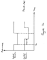
- the signal delay circuit 10 which, in the prior art, is used to generate a delay signal having a predetermined delay time, is shown.
- An input signal, SIGNAL IN is applied to a gate terminal of n-channel field-effect transistor 11 and to a gate terminal of p-channel field-effect transistor 12.
- the source terminal of transistor 12 is coupled to the V DD voltage supply terminal (V DD ), while the source terminal of transistor 11 is coupled to the ground potential.
- the drain terminal of transistor 12 is coupled to the drain terminal of transistor 11, to a first terminal of capacitor 13, and to an input terminal of inverting amplifier 14.
- the second terminal of capacitor 13 is coupled to the ground potential, while the output terminal of inverting amplifier 14 is the output signal, SIGNAL OUT, of the delay circuit.
- a comparison of an idealized input signal, SIGNAL IN, and an idealized output signal, SIGNAL OUT, of the delay circuit 10 is shown.
- the input signal has a negative-going step at a given time t o .
- the output signal provides a negative-going step delayed by a time, D, with respect to the negative-going step of the input signal.
- the time delay, D is a function of the size of capacitor C and the parameters of the semiconductor components.
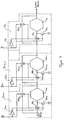
- Fig. 2 shows a configuration wherein a plurality of delay circuits 10' through 10''' are coupled in series.
- Each delay circuit is provided with switches, 21' through 21''' and 22' through 22'''.
- the switches 21' through 21''' and 22' through 22''' can be placed in an open or closed position.
- the state of the switches 21' through 21''' and 22' through 22''' determine which of the delay circuits 10' through 10'''' are electrically coupled in a series connection.
- the delay of SIGNAL OUT signal can be controlled during the fabrication by the removal of conducting paths.
- a relatively simple change in the fabrication process i.e. setting the state of the switches 21' through 21''' and 22' through 22''', can provide a controlled change in the delay time D.
- the setting of the switches in the fabrication process or in the case of setting of the switches through post fabrication processes such as with laser techniques, provides an improvement over the adjustment of parameters of an individual delay circuit, further improvement in the ability to control the delay time D is desirable.
- a plurality of time delay components each having a predetermined time delay, have gate units coupled thereto.
- the gate units in response to the state of an applied control signal, either electrically couple the component in a series configuration or remove the time delay component from the series configuration of the delay components.
- the resulting total time delay is the sum of the time delays of the time delay components coupled in the series configuration as a result of the control signals.
- control signals are applied to gate units coupled to a plurality of parallel-coupled resistors in a time delay component.
- the control signals determine which of the resistors is coupled to a capacitor.
- the delay time of the component between the input signal and the output signal is determined by the rate of charging of the capacitor through the electrically coupled resistors.
- a time delay component has a plurality of parallel-coupled capacitors, each capacitor having a gate element coupled thereto. The response to the an associated control signal, each capacitor is either electrically coupled in series with the other capacitors or electrically removed from the circuit.
- the time delay of the component is determined by the size of the capacitance, i.e., by the number of coupled capacitors being charged through capacitor-charging elements and by the parameters of the capacitor-charging elements.
- a longer time delay can be provided by including any of the embodiments in a ring configuration and using a counter unit to generate a delayed signal after a selected number of time delays by the time delay unit.
- Figs. 1a, 1b and 2 have been discussed with respect to the prior art.
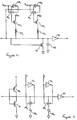
- the delay apparatus comprises a plurality of delay components 30 n through 30 o coupled in series.
- Each delay component 30 x includes a delay circuit 10 x .
- the signal terminals of a gate element 32 x is coupled between an input terminal of delay component 30 x and an output terminal of delay component 30 x .
- the output terminal of delay circuit 10 x is coupled to the output terminal of the delay component 30 x , while the input terminal of delay component 30 x is coupled through the signal terminal of gate element 33 x to an input terminal of delay circuit 10 x .
- the input terminal of gate 10 x is coupled through n-channel field effect transistor 34 x to the ground potential.
- a control signal b x is coupled to an input terminal of inverting amplifier 31 x , to the n-channel control terminal of gate element 32 x , to the p-channel control terminal of gate element 33 x , and to the gate terminal of transistor 34 x .
- the output terminal of inverting amplifier 31 x is coupled to the p-channel control terminal of gate element 32 x and to the n-channel control terminal of gate element 33 x .
- a second implementation of the programmable delay apparatus is shown.
- the INPUT SIGNAL is applied to a gate terminal of n-channel transistor 41.
- the drain terminal of transistor 41 is coupled to the input terminal of inverting amplifier 44, while the source terminal of transistor 41 is coupled to ground potential.
- the input terminal of inverting amplifier 44 is also coupled through capacitor 43 to the ground potential.
- the input terminal of inverting amplifier 44 is coupled to a series of resistors 47 n through 47 o .
- Each of the resistors 47 n through 47 o is coupled to the drain terminals of p-channel field effect transistors 42 n through 42 o , respectively.
- the source terminals of transistors 42 n through 42 o are coupled to the supply voltage V DD , while the gate terminals of each of transistors 42 n through 42 o is coupled to a first signal terminal of gate elements 42 n through 42 o , respectively.
- a second signal terminal of gate elements 46 n through 46 o receives the input signal.
- the control terminals of gate elements 46 n through 46 o are coupled to the input and the output terminals of inverting amplifiers 48 n through 48 o respectively.
- the input terminals of inverting amplifiers 48 n through 48 o have control signals b n through b o , respectively, applied thereto.
- the output terminal of inverting amplifier 44 supplies the OUTPUT SIGNAL.
- the INPUT SIGNAL is applied to a gate terminal of p-channel field effect transistor 52 and to a gate terminal of n-channel field effect transistor 51.
- a drain terminal of transistor 52 is coupled to an input terminal of inverting amplifier 54 and to a drain of transistor 51.
- the source terminal of transistor 51 is coupled to the ground potential.
- Also coupled to the input terminal of inverting amplifier 54 is a first signal terminal of a plurality of gate elements 55 n through 55 o .
- a second signal terminal of each of gate elements 55 n through 55 o is coupled through capacitors 53 n through 53 o , respectively, to the ground potential.
- control terminals of gate elements 55 n through 55 o are coupled to input and output terminals of inverting amplifiers 59 n through 59 o , respectively.
- the input terminals of each of inverting amplifiers 59 n through 59 o is coupled to control signals b n through b o , respectively.
- a programmable delay apparatus 61 has an input terminal coupled to an output terminal of inverting amplifier 62.
- An output terminal of programmable delay apparatus 61 is coupled to an input terminal of inverting amplifier 62, to an input terminal of counter unit 63, and to a reset terminal of latch unit 64.
- the output terminal of the counter unit 63 supplies the OUTPUT SIGNAL.
- the INPUT SIGNAL is applied to the latch unit 64 which initiates the operation, but prevents additional INPUT SIGNALS from affecting the operation until the output signal has reset the latch unit 64.
- each stage of the delay apparatus includes a delay circuit 10 n through 10 o .
- the sets of gate elements, 32 n through 32 o and 33 n through 33 o can either insert the delay circuits 10 n through 10 o in a series configuration or can electrically remove the delay circuits 10 n through 10 o from the series configuration depending on the state of the associated input signals b n through b o associated with each delay circuit.
- the delay time D of the delay apparatus is thus the sum of the delays times D n through D o for each of the delay circuits which are coupled in the series configuration.
- the delay time D of the apparatus is controlled by the resistors 47 n through 47 o through which the capacitor 43 is charged.
- the control signals determine which gate elements are activated.
- the activated gate elements in turn, establish which transistors are activated.
- the activated transistors place the resistors in the charging circuit of the capacitor 43.
- the resistors in the charging circuit determine the time constant of the charging operation and, consequently, determine the delay time D of the OUTPUT SIGNAL.
- the control signals b n through b o activate selected ones of the gate elements 55 n through 55 o .
- the activated gate elements couple selected capacitors 53 n through 53 o , each associated with the activated gate elements, to the input terminal of inverting amplifier 54.
- the coupled capacitors determine the charging time and therefore the delay time of the OUTPUT SIGNAL relative to the INPUT SIGNAL.
- the INPUT SIGNAL initiates the operation of the programmable delay apparatus.
- the output signal of the programmable delay apparatus after being counted by the counter unit, is applied to the input of the programmable delay apparatus.
- another count is entered in the counter unit.
- the OUTPUT SIGNAL is generated by the counter unit and the apparatus initialized in preparation for the next INPUT SIGNAL. In this manner, the delay time D can be expanded, reducing the number of elements required to provide desired range of delay times.
- the programmable delay apparatus of the present invention is provided by selectively coupling a plurality of elements, each providing a prestablished delay time, in response to control signals.
- the control signals can be generated internally or externally and can be stored in a latch circuit or in a register.
- the programmable delay apparatus can therefore be incorporated on every semiconductor chip and the exact value of the delay time selected after the fabrication. This programmable delay time can be used to compensate for variations in circuits resulting from the fabrication process. Further flexibility can be obtained by applying control signals to counter unit in the circuit described in relation to Fig. 6.
- each of the components which can be coupled into the programmable delay circuit need not provide the same delay. Rather the delay times of the individual components can be chosen to provide a requisite delay time accuracy over a predetermined range of delay times. It will also be clear that the delay for a positive signal edge can be provided with appropriate changes in the individual components. While the invention has been described with particular reference to the preferred embodiment, it will be understood by those skilled in the art that various changes may be made and equivalents substituted for elements of the preferred embodiment without departing from the invention. In addition, many modifications may be made to adapt a particular situation and material to a teaching of the present invention without departing from the essential teachings of the present invention.
Landscapes
- Physics & Mathematics (AREA)
- Nonlinear Science (AREA)
- Engineering & Computer Science (AREA)
- Microelectronics & Electronic Packaging (AREA)
- Computer Hardware Design (AREA)
- Pulse Circuits (AREA)
- Dram (AREA)
- Networks Using Active Elements (AREA)
- Logic Circuits (AREA)
Applications Claiming Priority (2)
| Application Number | Priority Date | Filing Date | Title |
|---|---|---|---|
| US767695P | 1995-11-29 | 1995-11-29 | |
| US7676 | 1995-11-29 |
Publications (3)
| Publication Number | Publication Date |
|---|---|
| EP0777232A2 true EP0777232A2 (de) | 1997-06-04 |
| EP0777232A3 EP0777232A3 (de) | 1999-08-04 |
| EP0777232B1 EP0777232B1 (de) | 2003-03-19 |
Family
ID=21727534
Family Applications (1)
| Application Number | Title | Priority Date | Filing Date |
|---|---|---|---|
| EP96118945A Expired - Lifetime EP0777232B1 (de) | 1995-11-29 | 1996-11-27 | Programmierbare Zeitverzögerung für oder in Beziehung auf Halbleiterspeicher |
Country Status (5)
| Country | Link |
|---|---|
| US (2) | US5841707A (de) |
| EP (1) | EP0777232B1 (de) |
| JP (2) | JPH09180445A (de) |
| KR (1) | KR970029840A (de) |
| DE (1) | DE69626752T2 (de) |
Families Citing this family (33)
| Publication number | Priority date | Publication date | Assignee | Title |
|---|---|---|---|---|
| IL96808A (en) * | 1990-04-18 | 1996-03-31 | Rambus Inc | Introductory / Origin Circuit Agreed Using High-Performance Brokerage |
| JP4198201B2 (ja) * | 1995-06-02 | 2008-12-17 | 株式会社ルネサステクノロジ | 半導体装置 |
| US6088774A (en) | 1996-09-20 | 2000-07-11 | Advanced Memory International, Inc. | Read/write timing for maximum utilization of bidirectional read/write bus |
| US5917760A (en) * | 1996-09-20 | 1999-06-29 | Sldram, Inc. | De-skewing data signals in a memory system |
| US5953263A (en) * | 1997-02-10 | 1999-09-14 | Rambus Inc. | Synchronous memory device having a programmable register and method of controlling same |
| US5940608A (en) | 1997-02-11 | 1999-08-17 | Micron Technology, Inc. | Method and apparatus for generating an internal clock signal that is synchronized to an external clock signal |
| US6912680B1 (en) | 1997-02-11 | 2005-06-28 | Micron Technology, Inc. | Memory system with dynamic timing correction |
| US5946244A (en) | 1997-03-05 | 1999-08-31 | Micron Technology, Inc. | Delay-locked loop with binary-coupled capacitor |
| US6173432B1 (en) | 1997-06-20 | 2001-01-09 | Micron Technology, Inc. | Method and apparatus for generating a sequence of clock signals |
| KR100261215B1 (ko) * | 1997-07-29 | 2000-07-01 | 윤종용 | 클럭 버퍼 및 이를 포함하는 메모리 로직 복합 반도체장치 |
| US6101197A (en) | 1997-09-18 | 2000-08-08 | Micron Technology, Inc. | Method and apparatus for adjusting the timing of signals over fine and coarse ranges |
| JPH11154398A (ja) * | 1997-11-20 | 1999-06-08 | Oki Electric Ind Co Ltd | 半導体記憶装置 |
| US6269451B1 (en) | 1998-02-27 | 2001-07-31 | Micron Technology, Inc. | Method and apparatus for adjusting data timing by delaying clock signal |
| US5923613A (en) * | 1998-03-18 | 1999-07-13 | Etron Technology, Inc. | Latched type clock synchronizer with additional 180°-phase shift clock |
| US6052746A (en) * | 1998-04-14 | 2000-04-18 | Motorola, Inc. | Integrated circuit having programmable pull device configured to enable/disable first function in favor of second function according to predetermined scheme before/after reset |
| US6338127B1 (en) | 1998-08-28 | 2002-01-08 | Micron Technology, Inc. | Method and apparatus for resynchronizing a plurality of clock signals used to latch respective digital signals, and memory device using same |
| US6279090B1 (en) | 1998-09-03 | 2001-08-21 | Micron Technology, Inc. | Method and apparatus for resynchronizing a plurality of clock signals used in latching respective digital signals applied to a packetized memory device |
| US6349399B1 (en) | 1998-09-03 | 2002-02-19 | Micron Technology, Inc. | Method and apparatus for generating expect data from a captured bit pattern, and memory device using same |
| US6430696B1 (en) | 1998-11-30 | 2002-08-06 | Micron Technology, Inc. | Method and apparatus for high speed data capture utilizing bit-to-bit timing correction, and memory device using same |
| US6374360B1 (en) | 1998-12-11 | 2002-04-16 | Micron Technology, Inc. | Method and apparatus for bit-to-bit timing correction of a high speed memory bus |
| US6470060B1 (en) | 1999-03-01 | 2002-10-22 | Micron Technology, Inc. | Method and apparatus for generating a phase dependent control signal |
| US6111812A (en) | 1999-07-23 | 2000-08-29 | Micron Technology, Inc. | Method and apparatus for adjusting control signal timing in a memory device |
| KR100355229B1 (ko) * | 2000-01-28 | 2002-10-11 | 삼성전자 주식회사 | 카스 명령의 동작 지연 기능을 구비한 반도체 메모리 장치및 이에 적용되는 버퍼와 신호전송 회로 |
| JP3647364B2 (ja) | 2000-07-21 | 2005-05-11 | Necエレクトロニクス株式会社 | クロック制御方法及び回路 |
| US6801989B2 (en) | 2001-06-28 | 2004-10-05 | Micron Technology, Inc. | Method and system for adjusting the timing offset between a clock signal and respective digital signals transmitted along with that clock signal, and memory device and computer system using same |
| KR100446291B1 (ko) * | 2001-11-07 | 2004-09-01 | 삼성전자주식회사 | 카스 레이턴시를 이용하여 락킹 레졸루션 조절이 가능한지연동기 루프 회로 |
| US7168027B2 (en) | 2003-06-12 | 2007-01-23 | Micron Technology, Inc. | Dynamic synchronization of data capture on an optical or other high speed communications link |
| US7068564B2 (en) * | 2003-06-29 | 2006-06-27 | International Business Machines Corporation | Timer lockout circuit for synchronous applications |
| US7234070B2 (en) | 2003-10-27 | 2007-06-19 | Micron Technology, Inc. | System and method for using a learning sequence to establish communications on a high-speed nonsynchronous interface in the absence of clock forwarding |
| US7283005B2 (en) * | 2004-02-10 | 2007-10-16 | Stmicroelectronics S.R.L. | Clock-pulse generator circuit |
| JP4960807B2 (ja) * | 2007-08-28 | 2012-06-27 | セイコーインスツル株式会社 | 可変周波数発振回路 |
| KR101144864B1 (ko) * | 2010-10-12 | 2012-05-14 | 알에프코어 주식회사 | 실시간 지연 장치 |
| CN114374377A (zh) * | 2022-01-11 | 2022-04-19 | 长鑫存储技术有限公司 | 延时电路 |
Family Cites Families (17)
| Publication number | Priority date | Publication date | Assignee | Title |
|---|---|---|---|---|
| JPS6059814A (ja) * | 1983-09-12 | 1985-04-06 | Hitachi Ltd | プログラマブル遅延回路およびこれを用いた半導体集積回路装置 |
| JPS61237512A (ja) * | 1985-04-12 | 1986-10-22 | Nec Ic Microcomput Syst Ltd | 半導体集積回路 |
| US4894626A (en) * | 1988-09-30 | 1990-01-16 | Advanced Micro Devices, Inc. | Variable length shift register |
| US5068553A (en) * | 1988-10-31 | 1991-11-26 | Texas Instruments Incorporated | Delay stage with reduced Vdd dependence |
| US5028824A (en) * | 1989-05-05 | 1991-07-02 | Harris Corporation | Programmable delay circuit |
| JPH03219719A (ja) * | 1990-01-24 | 1991-09-27 | Mitsubishi Electric Corp | 遅延回路及びそれを用いた半導体装置 |
| US5051630A (en) * | 1990-03-12 | 1991-09-24 | Tektronix, Inc. | Accurate delay generator having a compensation feature for power supply voltage and semiconductor process variations |
| US5202642A (en) * | 1991-05-09 | 1993-04-13 | Iomega Corporation | Apparatus and method for fractional frequency division |
| US5465076A (en) * | 1991-10-04 | 1995-11-07 | Nippondenso Co., Ltd. | Programmable delay line programmable delay circuit and digital controlled oscillator |
| JP2982928B2 (ja) * | 1992-04-01 | 1999-11-29 | 三菱電機株式会社 | 半導体記憶装置 |
| JPH0612877A (ja) * | 1992-06-18 | 1994-01-21 | Toshiba Corp | 半導体集積回路 |
| US5281927A (en) * | 1993-05-20 | 1994-01-25 | Codex Corp. | Circuit and method of controlling a VCO with capacitive loads |
| US5459422A (en) * | 1993-06-02 | 1995-10-17 | Advanced Micro Devices, Inc. | Edge selective delay circuit |
| FR2718903B1 (fr) * | 1994-04-13 | 1996-05-24 | Bull Sa | Circuit à retard réglable. |
| KR0138208B1 (ko) * | 1994-12-08 | 1998-04-28 | 문정환 | 반도체 메모리 소자 |
| JPH0969292A (ja) * | 1995-08-30 | 1997-03-11 | Nec Corp | 半導体記憶装置 |
| JPH1064275A (ja) * | 1996-08-27 | 1998-03-06 | Nkk Corp | 遅延回路、atdパルス発生回路、及びそれを用いた半導体記憶装置 |
-
1996
- 1996-11-25 US US08/758,138 patent/US5841707A/en not_active Expired - Lifetime
- 1996-11-27 EP EP96118945A patent/EP0777232B1/de not_active Expired - Lifetime
- 1996-11-27 DE DE69626752T patent/DE69626752T2/de not_active Expired - Lifetime
- 1996-11-28 KR KR1019960058916A patent/KR970029840A/ko not_active Ceased
- 1996-11-29 JP JP8320402A patent/JPH09180445A/ja not_active Withdrawn
-
1998
- 1998-07-31 US US09/127,391 patent/US6002286A/en not_active Expired - Lifetime
-
2007
- 2007-04-09 JP JP2007101792A patent/JP4279888B2/ja not_active Expired - Lifetime
Non-Patent Citations (1)
| Title |
|---|
| None |
Also Published As
| Publication number | Publication date |
|---|---|
| KR970029840A (ko) | 1997-06-26 |
| JP4279888B2 (ja) | 2009-06-17 |
| JPH09180445A (ja) | 1997-07-11 |
| JP2007228617A (ja) | 2007-09-06 |
| DE69626752D1 (de) | 2003-04-24 |
| DE69626752T2 (de) | 2003-11-20 |
| EP0777232B1 (de) | 2003-03-19 |
| EP0777232A3 (de) | 1999-08-04 |
| US5841707A (en) | 1998-11-24 |
| US6002286A (en) | 1999-12-14 |
Similar Documents
| Publication | Publication Date | Title |
|---|---|---|
| US6002286A (en) | Apparatus and method for a programmable interval timing generator in a semiconductor memory | |
| US5506534A (en) | Digitally adjustable picosecond delay circuit | |
| US5121014A (en) | CMOS delay circuit with controllable delay | |
| US4746823A (en) | Voltage-insensitive and temperature-compensated delay circuit for a monolithic integrated circuit | |
| US6204710B1 (en) | Precision trim circuit for delay lines | |
| US4800304A (en) | Time delay circuit for a semiconductor device | |
| EP0150480A2 (de) | Impulsgenerator zur Grundzustandseinstellung bei Netzeinschaltung | |
| WO1998058449A2 (en) | Programmable delay circuit having calibratable delays | |
| US4985639A (en) | Logic edge timing generation | |
| US5920221A (en) | RC delay circuit for integrated circuits | |
| KR100440448B1 (ko) | 온도 변화에 무관한 지연 시간을 확보할 수 있는 반도체집적 회로장치 | |
| JPH0812755B2 (ja) | 制御回路プリチャージ回路 | |
| US6476655B2 (en) | Semiconductor device | |
| US4924115A (en) | Integrated circuit RC filters with very large time constants | |
| US6346835B1 (en) | Power-on reset signal preparing circuit | |
| US5519666A (en) | Apparatus and method for an address transition detector | |
| US6867629B2 (en) | Integrated circuit and method of adjusting capacitance of a node of an integrated circuit | |
| JP4404756B2 (ja) | 半導体集積回路 | |
| US12301193B2 (en) | Pulse filter | |
| KR900007929B1 (ko) | 전압 램프 속도(Ramp Speed) 제어회로 | |
| KR100210847B1 (ko) | 노이즈 제거폭 가변형 회로 | |
| EP0735453A2 (de) | Verzögerungsschaltung und Verfahren | |
| JPH0520881A (ja) | 半導体出力回路 | |
| KR930009425B1 (ko) | 시스템 초기리세트회로 | |
| JP2806960B2 (ja) | 遅延回路 |
Legal Events
| Date | Code | Title | Description |
|---|---|---|---|
| PUAI | Public reference made under article 153(3) epc to a published international application that has entered the european phase |
Free format text: ORIGINAL CODE: 0009012 |
|
| AK | Designated contracting states |
Kind code of ref document: A2 Designated state(s): DE FR GB IT NL |
|
| PUAL | Search report despatched |
Free format text: ORIGINAL CODE: 0009013 |
|
| AK | Designated contracting states |
Kind code of ref document: A3 Designated state(s): DE FR GB IT NL |
|
| RIC1 | Information provided on ipc code assigned before grant |
Free format text: 6G 11C 7/00 A, 6G 11C 8/00 B, 6H 03K 5/13 B |
|
| 17P | Request for examination filed |
Effective date: 20000204 |
|
| 17Q | First examination report despatched |
Effective date: 20010412 |
|
| GRAH | Despatch of communication of intention to grant a patent |
Free format text: ORIGINAL CODE: EPIDOS IGRA |
|
| GRAH | Despatch of communication of intention to grant a patent |
Free format text: ORIGINAL CODE: EPIDOS IGRA |
|
| GRAA | (expected) grant |
Free format text: ORIGINAL CODE: 0009210 |
|
| AK | Designated contracting states |
Designated state(s): DE FR GB IT NL |
|
| PG25 | Lapsed in a contracting state [announced via postgrant information from national office to epo] |
Ref country code: NL Free format text: LAPSE BECAUSE OF FAILURE TO SUBMIT A TRANSLATION OF THE DESCRIPTION OR TO PAY THE FEE WITHIN THE PRESCRIBED TIME-LIMIT Effective date: 20030319 Ref country code: IT Free format text: LAPSE BECAUSE OF FAILURE TO SUBMIT A TRANSLATION OF THE DESCRIPTION OR TO PAY THE FEE WITHIN THE PRESCRIBED TIME-LIMIT;WARNING: LAPSES OF ITALIAN PATENTS WITH EFFECTIVE DATE BEFORE 2007 MAY HAVE OCCURRED AT ANY TIME BEFORE 2007. THE CORRECT EFFECTIVE DATE MAY BE DIFFERENT FROM THE ONE RECORDED. Effective date: 20030319 |
|
| REG | Reference to a national code |
Ref country code: GB Ref legal event code: FG4D |
|
| REF | Corresponds to: |
Ref document number: 69626752 Country of ref document: DE Date of ref document: 20030424 Kind code of ref document: P |
|
| NLV1 | Nl: lapsed or annulled due to failure to fulfill the requirements of art. 29p and 29m of the patents act | ||
| ET | Fr: translation filed | ||
| PLBE | No opposition filed within time limit |
Free format text: ORIGINAL CODE: 0009261 |
|
| STAA | Information on the status of an ep patent application or granted ep patent |
Free format text: STATUS: NO OPPOSITION FILED WITHIN TIME LIMIT |
|
| 26N | No opposition filed |
Effective date: 20031222 |
|
| PGFP | Annual fee paid to national office [announced via postgrant information from national office to epo] |
Ref country code: GB Payment date: 20101022 Year of fee payment: 15 |
|
| PGFP | Annual fee paid to national office [announced via postgrant information from national office to epo] |
Ref country code: FR Payment date: 20111103 Year of fee payment: 16 |
|
| PGFP | Annual fee paid to national office [announced via postgrant information from national office to epo] |
Ref country code: DE Payment date: 20111130 Year of fee payment: 16 |
|
| GBPC | Gb: european patent ceased through non-payment of renewal fee |
Effective date: 20121127 |
|
| REG | Reference to a national code |
Ref country code: FR Ref legal event code: ST Effective date: 20130731 |
|
| REG | Reference to a national code |
Ref country code: DE Ref legal event code: R119 Ref document number: 69626752 Country of ref document: DE Effective date: 20130601 |
|
| PG25 | Lapsed in a contracting state [announced via postgrant information from national office to epo] |
Ref country code: DE Free format text: LAPSE BECAUSE OF NON-PAYMENT OF DUE FEES Effective date: 20130601 |
|
| PG25 | Lapsed in a contracting state [announced via postgrant information from national office to epo] |
Ref country code: GB Free format text: LAPSE BECAUSE OF NON-PAYMENT OF DUE FEES Effective date: 20121127 Ref country code: FR Free format text: LAPSE BECAUSE OF NON-PAYMENT OF DUE FEES Effective date: 20121130 |