EP0762496A2 - Leistungshalbleitermodul - Google Patents
Leistungshalbleitermodul Download PDFInfo
- Publication number
- EP0762496A2 EP0762496A2 EP96810501A EP96810501A EP0762496A2 EP 0762496 A2 EP0762496 A2 EP 0762496A2 EP 96810501 A EP96810501 A EP 96810501A EP 96810501 A EP96810501 A EP 96810501A EP 0762496 A2 EP0762496 A2 EP 0762496A2
- Authority
- EP
- European Patent Office
- Prior art keywords
- contact
- main connection
- contact stamp
- main
- stamp
- Prior art date
- Legal status (The legal status is an assumption and is not a legal conclusion. Google has not performed a legal analysis and makes no representation as to the accuracy of the status listed.)
- Granted
Links
Images

Classifications
-
- H—ELECTRICITY
- H01—ELECTRIC ELEMENTS
- H01L—SEMICONDUCTOR DEVICES NOT COVERED BY CLASS H10
- H01L24/00—Arrangements for connecting or disconnecting semiconductor or solid-state bodies; Methods or apparatus related thereto
- H01L24/71—Means for bonding not being attached to, or not being formed on, the surface to be connected
- H01L24/72—Detachable connecting means consisting of mechanical auxiliary parts connecting the device, e.g. pressure contacts using springs or clips
-
- H—ELECTRICITY
- H01—ELECTRIC ELEMENTS
- H01L—SEMICONDUCTOR DEVICES NOT COVERED BY CLASS H10
- H01L25/00—Assemblies consisting of a plurality of semiconductor or other solid state devices
- H01L25/03—Assemblies consisting of a plurality of semiconductor or other solid state devices all the devices being of a type provided for in a single subclass of subclasses H10B, H10D, H10F, H10H, H10K or H10N, e.g. assemblies of rectifier diodes
- H01L25/04—Assemblies consisting of a plurality of semiconductor or other solid state devices all the devices being of a type provided for in a single subclass of subclasses H10B, H10D, H10F, H10H, H10K or H10N, e.g. assemblies of rectifier diodes the devices not having separate containers
- H01L25/07—Assemblies consisting of a plurality of semiconductor or other solid state devices all the devices being of a type provided for in a single subclass of subclasses H10B, H10D, H10F, H10H, H10K or H10N, e.g. assemblies of rectifier diodes the devices not having separate containers the devices being of a type provided for in group subclass H10D
- H01L25/072—Assemblies consisting of a plurality of semiconductor or other solid state devices all the devices being of a type provided for in a single subclass of subclasses H10B, H10D, H10F, H10H, H10K or H10N, e.g. assemblies of rectifier diodes the devices not having separate containers the devices being of a type provided for in group subclass H10D the devices being arranged next to each other
-
- H—ELECTRICITY
- H01—ELECTRIC ELEMENTS
- H01L—SEMICONDUCTOR DEVICES NOT COVERED BY CLASS H10
- H01L2224/00—Indexing scheme for arrangements for connecting or disconnecting semiconductor or solid-state bodies and methods related thereto as covered by H01L24/00
- H01L2224/01—Means for bonding being attached to, or being formed on, the surface to be connected, e.g. chip-to-package, die-attach, "first-level" interconnects; Manufacturing methods related thereto
- H01L2224/42—Wire connectors; Manufacturing methods related thereto
- H01L2224/47—Structure, shape, material or disposition of the wire connectors after the connecting process
- H01L2224/48—Structure, shape, material or disposition of the wire connectors after the connecting process of an individual wire connector
- H01L2224/4805—Shape
- H01L2224/4809—Loop shape
- H01L2224/48091—Arched
-
- H—ELECTRICITY
- H01—ELECTRIC ELEMENTS
- H01L—SEMICONDUCTOR DEVICES NOT COVERED BY CLASS H10
- H01L2224/00—Indexing scheme for arrangements for connecting or disconnecting semiconductor or solid-state bodies and methods related thereto as covered by H01L24/00
- H01L2224/01—Means for bonding being attached to, or being formed on, the surface to be connected, e.g. chip-to-package, die-attach, "first-level" interconnects; Manufacturing methods related thereto
- H01L2224/42—Wire connectors; Manufacturing methods related thereto
- H01L2224/47—Structure, shape, material or disposition of the wire connectors after the connecting process
- H01L2224/48—Structure, shape, material or disposition of the wire connectors after the connecting process of an individual wire connector
- H01L2224/481—Disposition
- H01L2224/48151—Connecting between a semiconductor or solid-state body and an item not being a semiconductor or solid-state body, e.g. chip-to-substrate, chip-to-passive
- H01L2224/48221—Connecting between a semiconductor or solid-state body and an item not being a semiconductor or solid-state body, e.g. chip-to-substrate, chip-to-passive the body and the item being stacked
- H01L2224/48245—Connecting between a semiconductor or solid-state body and an item not being a semiconductor or solid-state body, e.g. chip-to-substrate, chip-to-passive the body and the item being stacked the item being metallic
- H01L2224/48247—Connecting between a semiconductor or solid-state body and an item not being a semiconductor or solid-state body, e.g. chip-to-substrate, chip-to-passive the body and the item being stacked the item being metallic connecting the wire to a bond pad of the item
-
- H—ELECTRICITY
- H01—ELECTRIC ELEMENTS
- H01L—SEMICONDUCTOR DEVICES NOT COVERED BY CLASS H10
- H01L2924/00—Indexing scheme for arrangements or methods for connecting or disconnecting semiconductor or solid-state bodies as covered by H01L24/00
- H01L2924/01—Chemical elements
- H01L2924/01004—Beryllium [Be]
-
- H—ELECTRICITY
- H01—ELECTRIC ELEMENTS
- H01L—SEMICONDUCTOR DEVICES NOT COVERED BY CLASS H10
- H01L2924/00—Indexing scheme for arrangements or methods for connecting or disconnecting semiconductor or solid-state bodies as covered by H01L24/00
- H01L2924/01—Chemical elements
- H01L2924/01005—Boron [B]
-
- H—ELECTRICITY
- H01—ELECTRIC ELEMENTS
- H01L—SEMICONDUCTOR DEVICES NOT COVERED BY CLASS H10
- H01L2924/00—Indexing scheme for arrangements or methods for connecting or disconnecting semiconductor or solid-state bodies as covered by H01L24/00
- H01L2924/01—Chemical elements
- H01L2924/01029—Copper [Cu]
-
- H—ELECTRICITY
- H01—ELECTRIC ELEMENTS
- H01L—SEMICONDUCTOR DEVICES NOT COVERED BY CLASS H10
- H01L2924/00—Indexing scheme for arrangements or methods for connecting or disconnecting semiconductor or solid-state bodies as covered by H01L24/00
- H01L2924/01—Chemical elements
- H01L2924/01033—Arsenic [As]
-
- H—ELECTRICITY
- H01—ELECTRIC ELEMENTS
- H01L—SEMICONDUCTOR DEVICES NOT COVERED BY CLASS H10
- H01L2924/00—Indexing scheme for arrangements or methods for connecting or disconnecting semiconductor or solid-state bodies as covered by H01L24/00
- H01L2924/01—Chemical elements
- H01L2924/01042—Molybdenum [Mo]
-
- H—ELECTRICITY
- H01—ELECTRIC ELEMENTS
- H01L—SEMICONDUCTOR DEVICES NOT COVERED BY CLASS H10
- H01L2924/00—Indexing scheme for arrangements or methods for connecting or disconnecting semiconductor or solid-state bodies as covered by H01L24/00
- H01L2924/01—Chemical elements
- H01L2924/01068—Erbium [Er]
-
- H—ELECTRICITY
- H01—ELECTRIC ELEMENTS
- H01L—SEMICONDUCTOR DEVICES NOT COVERED BY CLASS H10
- H01L2924/00—Indexing scheme for arrangements or methods for connecting or disconnecting semiconductor or solid-state bodies as covered by H01L24/00
- H01L2924/01—Chemical elements
- H01L2924/01082—Lead [Pb]
-
- H—ELECTRICITY
- H01—ELECTRIC ELEMENTS
- H01L—SEMICONDUCTOR DEVICES NOT COVERED BY CLASS H10
- H01L2924/00—Indexing scheme for arrangements or methods for connecting or disconnecting semiconductor or solid-state bodies as covered by H01L24/00
- H01L2924/10—Details of semiconductor or other solid state devices to be connected
- H01L2924/11—Device type
- H01L2924/13—Discrete devices, e.g. 3 terminal devices
- H01L2924/1304—Transistor
- H01L2924/1305—Bipolar Junction Transistor [BJT]
- H01L2924/13055—Insulated gate bipolar transistor [IGBT]
Definitions
- the invention relates to the field of power electronics. It is based on a power semiconductor module according to the preamble of the first claim.
- Such a power semiconductor module is already described in US Pat. No. 5,221,851. It is a so-called pressure contact semiconductor module, in which several semiconductor chips are applied with their first main electrode to a base plate. The second main electrodes of the chips are contacted by a plurality of contact stamps. The base plate is connected to a first main connection and the contact stamps are connected to a second main connection. The main connections can be disc-shaped and held together by means of flanges. The pressure contact is in the form of a copper stamp, which presses on the individual chips.
- the problem with this arrangement is the requirement for the plane parallelism of the chip surfaces or the copper stamp.
- the plane parallelism required for a pressure contact is, for example, only a few micrometers for a circular disc with a diameter of 7 cm. It is very difficult to comply with this requirement in the case of an arrangement with a plurality of chips, since the individual chips with conventional soldering technology can hardly be soldered at a common height, let alone the plane-parallel soldering.
- the essence of the invention is therefore that the position of the or each contact stamp can be set individually in accordance with the distance from the or each semiconductor chip to the second main connection. Since the position of the contact stamps can be set individually for each semiconductor chip, the plane parallelism no longer plays such a large role.
- the contact stamps are movably mounted. Trained means are provided for adjusting the position. These can include, for example, a solder layer or a spring with any sliding contacts.
- the solder layer surrounds the contact stamp in bores provided for this purpose and serves both to mechanically fix the contact stamp and to make electrical contact.
- these are arranged in the bores which are provided for receiving the contact stamp.
- a sliding contact for example in the form of a sliding spring, can also be used to improve the electrical contact with a large number of individual lamellae made of electrically highly conductive material, can be provided along the side walls of the bores.
- Semiconductor modules in which the contact stamps are fixed by means of soldering are best produced in such a way that the semiconductor chips are first soldered onto the base plate.
- the base plate with the semiconductor chips is then inserted into the second main connection, which is equipped with at least one bore and with at least one contact stamp and solder layer interposed therebetween.
- the position of the base plate in relation to the second main connection is now fixed, and the semiconductor module is soldered with the second main connection pointing upward in a soldering furnace.
- the solder layer melts between the contact stamp and the second main connection and fixes the individual position of the contact stamp. This was set automatically due to gravity before the soldering process.
- the advantage of the invention is therefore that such high demands on the plane parallelism are no longer necessary.
- this allows the modules to be manufactured at low cost.
- the contacting of the chips by means of contact pins be they soldered on or pressurized by springs, ensures permanent and individual pressure on each individual chip.
- a permanent low-resistance contact resistance is achieved between the housing contacts and the chip.
- the bond wires melt through. This can lead to complete destruction of the component.
- the type of contacting according to the invention additionally offers the advantage that, if one of the internally connected chips fails, the entire nominal but also the short-circuit current can be conducted with low resistance over the defective chip.
- Figure 1 shows a first example of how the invention can be implemented.
- 1 designates a power semiconductor module which has a first and a second main connection 6, 7.
- the main connections 6, 7 can consist of a solid copper block.
- a base plate 5 is applied to the first main connection 6.
- This can be, for example, a molybdenum plate 14, a ceramic plate or a plate made of other suitable materials, which is fastened with a solder layer 16 on the first main connection 6.
- the cross section of the base plate is not important for the invention. It can be round or angular.
- Several, more generally at least one semiconductor chip 2 are soldered onto the base plate 5.
- the semiconductor chips are preferably IGBT chips or diode chips or a combination of these types of chips.
- the chips 2 have at least two main electrodes 3 and 4, which are contacted by the corresponding main connections 6 and 7.
- a control electrode which is connected to a control connection 1 via a connecting wire 13.
- the connecting wire 13 is bonded, for example, to the control electrode of the chip 2.
- One main electrode 4 is formed by the underside of the chip 2 and is in direct connection with the base plate 5.
- the other main electrode 3 of the semiconductor chips 2 is contacted by a number of contact stamps 8 corresponding to the number of chips.
- a problem with the power semiconductor modules is that it is difficult to solder the chips 2 to the same height.
- the high degree of plane parallelism is necessary for problem-free pressure contact.
- the differently thick solder layers 15 are shown exaggerated in FIG.
- the stacks consist of different heights consisting of solder layers, at most molybdenum disks and semiconductor chips inserted between them.
- the contact stamps 8 are movably arranged in their bores in the second main connection 7 before the actual assembly.
- a solder layer 9 is provided between the bore and the contact stamp 8 according to the first embodiment. During assembly, this solder layer is melted in a soldering furnace so that the contact stamps are fixed.
- An automatic adaptation of the contact stamp length to the individual distance between the second main connection 7 and the semiconductor chips 2 is easiest and preferably achieved by soldering the semiconductor module to the second main connection 7 upwards. The contact stamps 8 fall down due to gravity and contact the chips.
- a further solder layer 10 is provided between the chips 2 and the contact stamps 8, at most with a molybdenum disk interposed therebetween.
- This solder layer 10 is in the same step as the solder layer 9 soldered in the soldering furnace.
- the arrangement is surrounded by a fixing device which, after adjustment, ensures a precisely aligned connection of the contact stamps 8 on the chips 2 during the soldering process.
- a power semiconductor module constructed as described above can be installed, for example, in a pressure contact housing known from GTO technology.
- a support ring 12 is provided between the first and the second main connections 6 and 7. This relieves pressure on the chip's solder joints and contact stamps. Any control connection 11 provided is then best passed through the support ring 12.
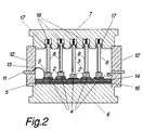
- FIG. 2 shows a further exemplary embodiment of a power semiconductor module according to the invention.
- the structure corresponds essentially to that of Figure 1, and corresponding parts are provided with the same reference numerals.
- a combination of springs 18 and a sliding contact 17 are provided.
- the springs are arranged in bores of the second main connection 7 and apply pressure to the contact stamps 8. In this way, the length of the contact stamp is set.
- sliding contact springs 17 can also be provided. These are arranged along the bore walls between the contact punches and the main connection.
- the spring sliding contacts can have a large number of individual lamellae.
- the contact stamps 8 loaded with spring pressure now press onto the chips 2.
- direct contacting of the chips 2 with the contact stamps is sufficient here 8 out.
- the power semiconductor module With the power semiconductor module according to the invention, it is also possible to construct different types of modules. Will like for example In the US patent mentioned at the outset, a combination of IGBT chips and diode chips is used to obtain a switch module in which the anti-parallel diode is integrated. However, it is also conceivable to integrate entire half or quarter bridge modules of converters in such a power semiconductor module or simply to build a high-performance diode.
- the invention is also not limited to IGBTs, but is used with advantage for all types of power semiconductor chips. Although the above description is based on a circular cross section of the module, the invention is not restricted to such cross sections.
- the invention results in a power semiconductor module in which the requirements for plane parallelism are less high than in the prior art and which can thus be manufactured and constructed more easily.
Landscapes
- Engineering & Computer Science (AREA)
- Power Engineering (AREA)
- Microelectronics & Electronic Packaging (AREA)
- Computer Hardware Design (AREA)
- Physics & Mathematics (AREA)
- Condensed Matter Physics & Semiconductors (AREA)
- General Physics & Mathematics (AREA)
- Die Bonding (AREA)
Abstract
Description
- Die Erfindung bezieht sich auf das Gebiet der Leistungselektronik. Sie geht aus von einem Leistungshalbleitermodul nach dem Oberbegriff des ersten Anspruchs.
- Ein solches Leistungshalbleitermodul wird schon im US Patent mit der Nummer 5,221,851 beschrieben. Es handelt sich dabei um sogenanntes Druckkontakt-Halbleitermodul, bei welchem mehrere Halbleiterchips mit ihrer ersten Hauptelektrode auf einer Grundplatte aufgebracht sind. Die zweiten Hauptelektroden der Chips werden von einer Mehrzahl von Kontaktstempeln kontaktiert. Die Grundplatte ist mit einem ersten Hauptanschluss und die Kontaktstempel sind mit einem zweiten Hauptanschluss verbunden. Die Hauptanschlüsse können scheibenförmig ausgebildet sein und mittels Flanschen zusammengehalten werden. Der Druckkontakt ist also in Form eines Kupferstempels ausgebildet, welcher auf die einzelnen Chips drückt.
- Problematisch bei dieser Anordnung sind jedoch die Anforderung an die Planparallelität der Chipoberflächen bzw. der Kupferstempel. Die für einen Druckkontakt benötigte Planparallelität beträgt beispielsweise bei einer kreisrunden Scheibe mit einem Durchmesser von 7 cm nur wenige Mikrometer. Diese Anforderung bei einer Anordnung mit einer Mehrzahl von Chips einzuhalten ist sehr schwierig, da die einzelnen Chips mit konventioneller Löttechnik praktisch kaum auf einer gemeinsamen Höhe geschweige den planparallel gelötet werden können.
- Aufgabe der vorliegenden Erfindung ist es deshalb, ein Leistungshalbleitermodul anzugeben, bei welchem weniger hohe Anforderungen an die Planparallelität gestellt werden.
- Diese Aufgabe wird bei einem Leistungshalbleitermodul der eingangs genannten Art durch die Merkmale des ersten Anspruchs gelöst.
- Kern der Erfindung ist es also, dass die Lage des oder jedes Kontaktstempels entsprechend dem Abstand von dem oder jedem Halbleiterchip zum zweiten Hauptanschluss individuell eingestellt werden kann. Da die Lage der Kontaktstempel für jeden Halbleiterchip individuell eingestellt werden kann, spielt die Planparallelität keine derart grosse Rolle mehr.
- Die Kontaktstempel sind beweglich gelagert. Zur Einstellung der Position sind dafür ausgebildete Mittel vorgesehen. Diese können beispielsweise eine Lotschicht oder eine Feder mit allfälligen Gleitkontakten umfassen. Die Lotschicht umgibt den Kontaktstempel in dafür vorgesehenen Bohrungen und dient sowohl der mechanischen Fixierung der Kontaktstempel als auch der elektrischen Kontaktierung. Bei der Variante mit den Federn sind diese in den Bohrungen angeordnet, welche für die Aufnahme der Kontaktstempel vorgesehen sind. Zur Verbesserung des elektrischen Kontaktes können ausserdem ein Gleitkontakt, z.B. in Form einer Gleitfeder mit einer Vielzahl von Einzellamellen aus elektrisch gut leitendem Material, entlang der Seitenwände der Bohrungen vorgesehen werden.
- Halbleitermodule, bei welchen die Kontaktstempel mittels Lötung fixiert werden, werden am besten so hergestellt, dass zunächst die Halbleiterchips auf die Grundplatte aufgelötet werden. Anschliessend wird die Grundplatte mit den Halbleiterchips in den mit mindestens einer Bohrung und mit mindestens einem Kontaktstempel und dazwischen gefügter Lotschicht bestückten zweiten Hauptanschluss eingesetzt. Die Lage der Grundplatte zum zweiten Hauptanschluss wird nun fixiert, und das Halbleitermodul mit nach oben weisendem zweiten Hauptanschluss in einem Lötofen verlötet. Dabei schmilzt die Lotschicht zwischen dem Kontaktstempel und dem zweiten Hauptanschluss und fixiert die individuelle Position der Kontaktstempel. Diese wurde aufgrund der Schwerkraft vor dem Lötvorgang automatisch eingestellt.
- Der Vorteil der Erfindung liegt also darin, dass keine derart hohen Anforderungen an die Planparallelität mehr notwendig sind. Dies erlaubt insbesondere eine kostengünstige Herstellung der Module. Ausserdem gewährleistet die Kontaktierung der Chips mittels Kontaktbolzen, seien diese angelötet oder mittels Federn mit Druck beaufschlagt, für einen permanenten und individuellen Druck auf jeden einzelnen Chip. Insbesondere im Falle, dass das Modul oder Teile davon im Falle eines Fehlers aufschmelzen, wird dadurch ein permanenter niederohmige Übergangswiderstand zwischen den Gehäusekontakten und dem Chip erreicht. Beim Stand der Technik schmelzen die Bonddrähte durch. Dies kann zu einer vollständigen Zerstörung des Bauelements führen. Somit bietet die erfindungsgemässe Art der Kontaktierung zusätzlich den Vorteil, dass bei Ausfall eines der intern parallelgeschalteten Chips der ganze Nominal- aber auch der Kurzschlussstrom niederohmig über den defekten Chip geleitet werden kann.
- Weitere Ausführungsbeispiele ergeben sich aus den entsprechenden abhängigen Ansprüchen.
- Nachfolgend wird die Erfindung anhand von Ausführungsbeispielen im Zusammenhang mit den Zeichnungen näher erläutert.
- Es zeigen:
- Fig. 1
- Einen Schnitt durch ein erfindungsgemässes Leistungshalbleitermodul nach einer ersten Ausführungsform; und
- Fig. 2
- Einen Schnitt durch ein erfindungsgemässes Leistungshalbleitermodul nach einer zweiten Ausführungsform.
- Die in den Zeichnungen verwendeten Bezugszeichen und deren Bedeutung sind in der Bezeichnungsliste zusammengefasst aufgelistet. Grundsätzlich sind in den Figuren gleiche Teile mit gleichen Bezugszeichen versehen.
- Figur 1 zeigt ein erstes Beispiel, wie die Erfindung realisiert werden kann. Mit 1 ist ein Leistungshalbleitermodul bezeichnet, welches einen ersten und einen zweiten Hauptanschluss 6, 7 aufweist. Die Hauptanschlüsse 6,7 können aus einem massiven Kupferblock bestehen. Auf den ersten Hauptanschluss 6 ist eine Grundplatte 5 aufgebracht. Dies kann beispielsweise eine Molybdänplatte 14, eine Keramikplatte oder ein Platte aus anderen geeigneten Materialien sein, welche mit einer Lotschicht 16 auf dem ersten Hauptanschluss 6 befestigt ist. Der Querschnitt der Grundplatte ist für die Erfindung nicht von Bedeutung. Er kann rund oder eckig sein. Auf die Grundplatte 5 sind mehrere, allgemeiner mindestens ein Halbleiterchip 2 aufgelötet. Vorzugsweise handelt es sich bei den Halbleiterchips um IGBT-Chips oder um Diodenchips oder um eine Kombination dieser Arten von Chips. Grundsätzlich weisen die Chips 2 jedoch mindestens zwei Hauptelektroden 3 und 4 auf, welche von den entsprechenden Hauptanschlüssen 6 und 7 kontaktiert werden. Im Falle von IGBT-Chips ist noch eine dritte Elektrode, eine Steuerelektrode vorgesehen, welche über einen Anschlussdraht 13 mit einem Steueranschluss 1 verbunden ist. Der Anschlussdraht 13 wird z.B. auf die Steuerelektrode des Chips 2 gebondet. Die eine Hauptelektrode 4 wird durch die Unterseite des Chips 2 gebildet und steht in direkter Verbindung mit der Grundplatte 5.
- Die andere Hauptelektrode 3 der Halbleiterchips 2 wird von einer der Anzahl Chips entsprechenden Anzahl von Kontaktstempeln 8 kontaktiert. Wie eingangs bereits erläutert wurde, besteht ein Problem bei den Leistungshalbleitermodulen darin, dass es Schwierigkeiten bereitet, die Chips 2 auf dieselbe Höhe anzulöten. Der hohe Grad an Planparallelität ist jedoch für einen problemlosen Druckkontakt notwendig. Um die Problematik deutlich zu machen, sind in Figur 1 die unterschiedlich dicken Lötschichten 15 überzeichnet dargestellt. Auch im Falle von unterschiedlich dicken Chips, z.B. bei einer Kombination von verschiedenen Chiptypen, ergibt sich eine unterschiedliche Höhe der Stapel bestehend aus Lötschichten, allenfalls dazwischen gefügten Molybdänscheiben und Halbleiterchips. Mit der Erfindung gelingt es nun, ein Leistungshalbleitermodul zu bauen, bei welchem diese Unterschied keinen Nachteil mehr darstellen.
- Dies wird dadurch erreicht, dass die Kontaktstempel 8 vor der eigentlichen Montage beweglich in ihren Bohrungen des zweiten Hauptanschlusses 7 angeordnet sind. Um die Kontaktstempel nach der Montage fixieren zu können, ist zwischen der Bohrung und dem Kontaktstempel 8 nach dem ersten Ausführungsbeispiel eine Lotschicht 9 vorgesehen. Bei der Montage wird diese Lotschicht in einem Lötofen zum Schmelzen gebracht, so dass die Kontaktstempel fixiert werden. Eine selbsttätige Anpassung der Kontaktstempel-Länge an den individuellen Abstand zwischen dem zweiten Hauptanschluss 7 und den Halbleiterchips 2 erreicht man am einfachsten und vorzugsweise dadurch, dass das Halbleitermodul mit dem zweiten Hauptanschluss 7 nach oben verlötet wird. Die Kontaktstempel 8 fallen durch die Schwerkraft nach unten und kontaktieren die Chips. Zwischen den Chips 2 und den Kontaktstempeln 8 ist eine weitere Lotschicht 10, allenfalls mit dazwischengefügter Molybdänscheibe vorgesehen. Diese Lotschicht 10 wird im gleichen Arbeitsschritt wie die Lotschicht 9 im Lötofen verlötet. Um die Lage des ersten Hauptanschlusses gegenüber dem zweiten Hauptanschluss zu fixieren, wird die Anordnung mit einer Fixiervorrichtung umgeben, welche nach erfolgter Justierung eine präzise ausgerichtete Verbindung der Kontaktstempel 8 auf den Chips 2 während des Lötvorganges gewährleistet.
- Ein wie oben beschrieben aufgebautes Leistungshalbleitermodul kann beispielsweise in ein von der GTO-Technologie bekanntes Druckkontaktgehäuse eingebaut werden. In diesem Fall ist es von Vorteil, wenn zwischen dem ersten und dem zweiten Hauptanschluss 6 und 7 ein Stützring 12 vorgesehen ist. Dieser entlastet die Lötstellen des Chips und die Kontaktstempel vom Druck. Ein allfällig vorgesehener Steueranschluss 11 wird dann am besten durch den Stützring 12 hindurchgeführt.
- Figur 2 zeigt ein weiteres Ausführungsbeispiel eines erfindungsgemässen Leistungshalbleitermoduls. Der Aufbau entspricht im wesentlichen demjenigen nach Figur 1, und entsprechende Teile sind mit denselben Bezugszeichen versehen. Zur Fixierung und Einstellung der Länge der Kontaktstempel 8 sind hier aber nicht Lotschichten 9, sondern eine Kombination von Federn 18 und einem Gleitkontakt 17 vorgesehen. Die Federn sind in Bohrungen des zweiten Hauptanschlusses 7 angeordnet und beaufschlagen die Kontaktstempel 8 mit Druck. Auf diese Art wird die Länge der Kontaktstempel eingestellt. Zur Verbesserung des elektrischen Kontaktes zwischen den Kontaktstempeln 8 und dem zweiten Hauptanschluss 7 können ausserdem Gleitkontaktfedern 17 vorgesehen werden. Diese sind entlang der Bohrungswände zwischen den Kontaktstempeln und dem Hauptanschluss angeordnet. Die Federgleitkontakte können eine Vielzahl von Einzellamellen aufweisen.
- Die mit Federdruck beaufschlagten Kontaktstempel 8 pressen nun auf die Chips 2. Im Gegensatz zum ersten Ausführungsbeispiel, in welchem zur Kontaktierung der Chips 2 eine Kombination von Lotschichten 10 und Mo-Plättchen 14 benötigt wird, reicht hier eine direkte Kontaktierung der Chips 2 mit den Kontaktstempeln 8 aus.
- Mit dem erfindungsgemässen Leistungshalbleitermodul ist es auch möglich, verschiedene Typen von Modulen aufzubauen. Wird wie beispielsweise in der eingangs genannte US Patentschrift eine Kombination von IGBT-Chips und Dioden-Chips verwendet, so erhält man ein Schaltermodul, bei welchem die Antiparalleldiode integriert ist. Es jedoch auch denkbar, ganze Halb- oder Viertelbrückenmodule von Umrichtern in einem solchen Leistungshalbleitermodul zu integrieren oder einfach nur eine Hochleistungsdiode zu bauen. Die Erfindung ist im übrigen auch nicht auf IGBTs beschränkt, sondern wird für alle Arten von Leistungshalbleiterchips mit Vorteil eingesetzt. Obwohl die vorstehende Beschreibung von einem kreisrunden Querschnitt des Moduls ausgeht, ist die Erfindung nicht auf solche Querschnitte beschränkt.
- Insgesamt ergibt sich mit der Erfindung ein Leistungshalbleitermodul, bei welchem die Anforderungen an die Planparallelität weniger hoch sind als beim Stand der Technik und welches somit einfacher hergestellt und aufgebaut werden kann.
-
- 1
- Leistungshalbleitermodul
- 2
- Halbleiterchips
- 3, 4
- Elektroden
- 5
- Grundplatte
- 6. 7
- Hauptanschlüsse
- 8
- Kontaktstempel
- 9, 10
- Lotschicht
- 11
- Steueranschluss
- 12
- Stützring
- 13
- Anschlussdraht
- 14
- Molybdänplatte
- 15, 16
- Lotschicht
- 17
- Gleitkontakt
- 18
- Feder
Claims (5)
- Leistungshalbleitermodul (1) mit mindestens einem Halbleiterchip (2), welcher oder welche mindestens zwei Elektroden, nämlich eine erste (4) und eine zweite Hauptelektrode (3), aufweisen und welcher oder welche Halbleiterchips (2) mit der ersten Hauptelektrode (4) auf einer Grundplatte (5) angebracht sind, und mit einem ersten und einem zweiten, mit den entsprechenden ersten und zweiten Hauptelektroden (4 bzw. 3) in elektrischer Verbindung stehenden Hauptanschluss (6 bzw. 7), wobei der erste Hauptanschluss (6) mit der Grundplatte (5) elektrisch zusammenwirkt und der zweite Hauptanschluss (7) mindestens einen Kontaktstempel (8) aufweist, welcher oder welche mit der zweiten (3) Hauptelektrode des oder jedes Halbleiterchips (2) elektrisch zusammenwirken, dadurch gekennzeichnet, dass eine Lage des oder jedes Kontaktstempels (8) entsprechend dem Abstand von dem oder jedem Halbleiterchip (2) zum zweiten Hauptanschluss (7) eingestellt werden kann und dass Mittel (9, 10; 17, 18) zur Fixierung der Lage des oder jedes Kontaktstempels (8) vorgesehen sind.
- Leistungshalbleitermodul nach Anspruch 1, dadurch gekennzeichnet, dass die Mittel zur Fixierung des oder jedes Kontaktstempels (8) zwei Lotschichten (9, 10) umfassen, welche einerseits zwischen dem oder jedem Halbleiterchip (2) und dem oder jedem Kontaktstempel (8) und andererseits zwischen dem oder jedem Kontaktstempel (8) und einer den oder jeden Kontaktstempel aufnehmenden Bohrung im zweiten Hauptanschluss (7) vorgesehen sind.
- Leistungshalbleitermodul nach Anspruch 1, dadurch gekennzeichnet, dass die Mittel zur Fixierung des oder jedes Kontaktstempels (8) für jeden Kontaktstempel eine Feder (18) umfassen, welche in einer den oder jeden Kontaktstempel aufnehmenden Bohrung im zweiten Hauptanschluss (7) angeordnet ist.
- Leistungshalbleitermodul nach Anspruch 3, dadurch gekennzeichnet, dass zwischen den Kontaktstempeln (8) und den Seitenwänden der Bohrungen elektrisch leitende Gleitfedern vorgesehen sind.
- Verfahren zur Herstellung eines Halbleitermoduls nach Anspruch 2, dadurch gekennzeichnet, dass- in einem ersten Schritt der oder jeder Halbleiterchip (2) auf die Grundplatte (5) gelötet wird;- die Grundplatte (5) auf den mit mindestens einer Bohrung, in welche je ein Kontaktstempel (8) eingefügt ist, versehenen zweiten Hauptanschluss (7) aufgesetzt und bezüglich des zweiten Hauptanschlusses (7) fixiert wird, wobei einerseits zwischen dem oder jedem Kontaktstempel (8) und dem oder jedem Halbleiterchip (2) und andererseits in jeder Bohrung zwischen dem oder jedem Kontaktstempel (8) und dem zweiten Hauptanschluss (7) je eine Lotschicht (10 bzw. 9) eingelegt wird;- das Halbleitermodul anschliessend mit dem zweiten Hauptanschluss (7) nach oben in einem Lötofen verlötet wird.
Applications Claiming Priority (2)
| Application Number | Priority Date | Filing Date | Title |
|---|---|---|---|
| DE19530264 | 1995-08-17 | ||
| DE19530264A DE19530264A1 (de) | 1995-08-17 | 1995-08-17 | Leistungshalbleitermodul |
Publications (3)
| Publication Number | Publication Date |
|---|---|
| EP0762496A2 true EP0762496A2 (de) | 1997-03-12 |
| EP0762496A3 EP0762496A3 (de) | 1999-05-06 |
| EP0762496B1 EP0762496B1 (de) | 2005-07-13 |
Family
ID=7769712
Family Applications (1)
| Application Number | Title | Priority Date | Filing Date |
|---|---|---|---|
| EP96810501A Expired - Lifetime EP0762496B1 (de) | 1995-08-17 | 1996-07-26 | Leistungshalbleitermodul |
Country Status (6)
| Country | Link |
|---|---|
| US (1) | US5705853A (de) |
| EP (1) | EP0762496B1 (de) |
| JP (1) | JP4020990B2 (de) |
| CN (1) | CN1089493C (de) |
| DE (2) | DE19530264A1 (de) |
| IN (1) | IN192638B (de) |
Cited By (6)
| Publication number | Priority date | Publication date | Assignee | Title |
|---|---|---|---|---|
| EP1209742A1 (de) * | 2000-11-22 | 2002-05-29 | ABB Schweiz AG | Hochleistungshalbleitermodul sowie Anwendung eines solchen Hochleistungshalbleitermoduls |
| EP1318545A1 (de) * | 2001-12-06 | 2003-06-11 | Abb Research Ltd. | Leistungshalbleiter-Submodul und Leistungshalbleiter-Modul |
| US6738258B2 (en) | 2001-12-06 | 2004-05-18 | Abb Research Ltd | Power semiconductor module |
| WO2004109801A1 (de) * | 2003-06-10 | 2004-12-16 | Eupec | Leistungshalbleitermodul |
| US7656672B2 (en) | 2003-11-11 | 2010-02-02 | Infineon Technologies Ag | Power module |
| EP3926670A1 (de) | 2020-06-15 | 2021-12-22 | Siemens Aktiengesellschaft | Leistungshalbleitermodul mit zumindest einem leistungshalbleiterelement |
Families Citing this family (44)
| Publication number | Priority date | Publication date | Assignee | Title |
|---|---|---|---|---|
| KR100214560B1 (ko) * | 1997-03-05 | 1999-08-02 | 구본준 | 반도체 멀티칩 모듈 |
| DE19726534A1 (de) * | 1997-06-23 | 1998-12-24 | Asea Brown Boveri | Leistungshalbleitermodul mit geschlossenen Submodulen |
| GB9725960D0 (en) * | 1997-12-08 | 1998-02-04 | Westinghouse Brake & Signal | Encapsulating semiconductor chips |
| DE19834800C1 (de) * | 1998-08-01 | 1999-10-28 | Semikron Elektronik Gmbh | Leistungshalbleiterschaltungsanordnung |
| JP3955396B2 (ja) * | 1998-09-17 | 2007-08-08 | 株式会社ルネサステクノロジ | 半導体サージ吸収素子 |
| DE19843309A1 (de) * | 1998-09-22 | 2000-03-23 | Asea Brown Boveri | Kurzschlussfestes IGBT Modul |
| DE19903245A1 (de) * | 1999-01-27 | 2000-08-03 | Asea Brown Boveri | Leistungshalbleitermodul |
| US6018194A (en) * | 1999-06-07 | 2000-01-25 | Lucent Technologies Inc. | Transistor clamping fixture |
| DE10064194B4 (de) * | 2000-12-22 | 2006-12-07 | Infineon Technologies Ag | Leistungshalbleiter-Modul und Kühlkörper zur Aufnahme des Leistungshalbleiter-Moduls |
| EP1263045A1 (de) * | 2001-06-01 | 2002-12-04 | ABB Schweiz AG | Leistungshalbleitermodul |
| EP1263046A1 (de) * | 2001-06-01 | 2002-12-04 | ABB Schweiz AG | Kontaktanordnung |
| DE10149886A1 (de) * | 2001-10-10 | 2003-04-30 | Eupec Gmbh & Co Kg | Leistunghalbleitermodul |
| DE10244748A1 (de) * | 2002-09-25 | 2003-09-11 | Siemens Ag | Leistungshalbleitermodul und Verfahren zur Herstellung desselben |
| DE102004018476B4 (de) * | 2004-04-16 | 2009-06-18 | Infineon Technologies Ag | Leistungshalbleiteranordnung mit kontaktierender Folie und Anpressvorrichtung |
| JP4977828B2 (ja) * | 2005-03-30 | 2012-07-18 | エスティー‐エリクソン、ソシエテ、アノニム | 携帯型物体接続可能パッケージ |
| DE102007003587B4 (de) * | 2007-01-24 | 2009-06-10 | Semikron Elektronik Gmbh & Co. Kg | Leistungshalbleitermodul mit Druckkörper |
| CA2718935C (en) | 2008-03-20 | 2016-05-10 | Abb Technology Ag | A voltage source converter |
| BRPI0822496A2 (pt) * | 2008-03-20 | 2015-06-16 | Abb Res Ag | Conversor de fonte de voltagem |
| DE102008033852B3 (de) * | 2008-07-19 | 2009-09-10 | Semikron Elektronik Gmbh & Co. Kg | Anordnung mit einem Leistungshalbleitermodul und Verfahren zu deren Herstellung |
| US7817422B2 (en) * | 2008-08-18 | 2010-10-19 | General Electric Company | Heat sink and cooling and packaging stack for press-packages |
| US8120915B2 (en) * | 2008-08-18 | 2012-02-21 | General Electric Company | Integral heat sink with spiral manifolds |
| US20100038774A1 (en) * | 2008-08-18 | 2010-02-18 | General Electric Company | Advanced and integrated cooling for press-packages |
| JP4634498B2 (ja) * | 2008-11-28 | 2011-02-16 | 三菱電機株式会社 | 電力用半導体モジュール |
| US8742814B2 (en) | 2009-07-15 | 2014-06-03 | Yehuda Binder | Sequentially operated modules |
| US8602833B2 (en) | 2009-08-06 | 2013-12-10 | May Patents Ltd. | Puzzle with conductive path |
| US8218320B2 (en) | 2010-06-29 | 2012-07-10 | General Electric Company | Heat sinks with C-shaped manifolds and millichannel cooling |
| US9597607B2 (en) | 2011-08-26 | 2017-03-21 | Littlebits Electronics Inc. | Modular electronic building systems with magnetic interconnections and methods of using the same |
| US11330714B2 (en) | 2011-08-26 | 2022-05-10 | Sphero, Inc. | Modular electronic building systems with magnetic interconnections and methods of using the same |
| US9019718B2 (en) | 2011-08-26 | 2015-04-28 | Littlebits Electronics Inc. | Modular electronic building systems with magnetic interconnections and methods of using the same |
| EP2769410B8 (de) * | 2011-10-21 | 2022-01-05 | Hitachi Energy Switzerland AG | Leistungshalbleitermodul und leistungshalbleitermodulanordnung mit mehreren leistungshalbleitermodulen |
| FR2994333B1 (fr) | 2012-08-03 | 2014-08-01 | Ge Energy Power Conversion Technology Ltd | Dispositif electronique semi-conducteur destine a etre monte dans un ensemble a empilement presse et ensemble a empilement presse comportant un tel dispositif |
| US8987876B2 (en) * | 2013-03-14 | 2015-03-24 | General Electric Company | Power overlay structure and method of making same |
| JP6043238B2 (ja) * | 2013-04-26 | 2016-12-14 | 株式会社豊田中央研究所 | 半導体モジュール |
| JP5819880B2 (ja) * | 2013-05-08 | 2015-11-24 | 本田技研工業株式会社 | 平行度調整装置および平行度調整方法 |
| JP6480098B2 (ja) | 2013-10-31 | 2019-03-06 | 三菱電機株式会社 | 半導体装置 |
| JP6189798B2 (ja) * | 2014-07-08 | 2017-08-30 | 日立オートモティブシステムズ株式会社 | 電力変換装置 |
| CN105336723B (zh) | 2014-07-28 | 2018-09-14 | 通用电气公司 | 半导体模块、半导体模块组件及半导体装置 |
| WO2016189953A1 (ja) * | 2015-05-26 | 2016-12-01 | 三菱電機株式会社 | 圧接型半導体装置 |
| JP6699737B2 (ja) * | 2016-09-09 | 2020-05-27 | 三菱電機株式会社 | 半導体装置 |
| DE112016007212B4 (de) | 2016-09-13 | 2025-03-27 | Mitsubishi Electric Corporation | Halbleitermodul |
| JP6688198B2 (ja) * | 2016-09-27 | 2020-04-28 | 日本発條株式会社 | 圧接ユニットおよび電力用半導体装置 |
| CN108428677B (zh) * | 2018-03-16 | 2020-09-11 | 全球能源互联网研究院有限公司 | 一种压接型igbt弹性压装结构及压接型igbt封装结构 |
| EP3696854A1 (de) * | 2019-02-13 | 2020-08-19 | Siemens Aktiengesellschaft | Leistungshalbleitermodul und verfahren zur herstellung eines leistungshalbleitermoduls |
| US11616844B2 (en) | 2019-03-14 | 2023-03-28 | Sphero, Inc. | Modular electronic and digital building systems and methods of using the same |
Family Cites Families (23)
| Publication number | Priority date | Publication date | Assignee | Title |
|---|---|---|---|---|
| CA804796A (en) * | 1969-01-21 | Emeis Reimer | Encapsulated electronic semiconductor device | |
| US3064341A (en) * | 1956-12-26 | 1962-11-20 | Ibm | Semiconductor devices |
| NL293539A (de) * | 1962-06-09 | |||
| DE1295696B (de) * | 1963-03-06 | 1969-05-22 | Walter Brandt Gmbh | Anordnung mit zwischen Kuehlplatten liegenden Halbleiterbauelementen |
| GB1054422A (de) * | 1963-03-16 | 1900-01-01 | ||
| GB1055673A (en) * | 1964-03-31 | 1967-01-18 | Ckd Praha Narodnt Podnik | Improved electrode connections in a semi-conductor housing |
| US3972012A (en) * | 1974-12-23 | 1976-07-27 | Rca Corporation | Apparatus for mounting a diode in a microwave circuit |
| US4179802A (en) * | 1978-03-27 | 1979-12-25 | International Business Machines Corporation | Studded chip attachment process |
| DE2832040A1 (de) * | 1978-07-21 | 1980-01-31 | Licentia Gmbh | Eingehaeuster, mit licht zuendbarer thyristor |
| US4278990A (en) * | 1979-03-19 | 1981-07-14 | General Electric Company | Low thermal resistance, low stress semiconductor package |
| DE2936816A1 (de) * | 1979-08-17 | 1981-03-26 | BBC Aktiengesellschaft Brown, Boveri & Cie., Baden, Aargau | Buerstenkontakt fuer leistungshalbleiterbauelemente |
| US4574299A (en) * | 1981-03-02 | 1986-03-04 | General Electric Company | Thyristor packaging system |
| US4646131A (en) * | 1983-01-28 | 1987-02-24 | Mitsubishi Denki Kabushiki Kaisha | Rectifier device |
| DE3322593A1 (de) * | 1983-06-23 | 1985-01-10 | Klöckner-Moeller Elektrizitäts GmbH, 5300 Bonn | Halbleiteranordnung und verfahren zu ihrer herstellung |
| JPS6089946A (ja) * | 1983-10-24 | 1985-05-20 | Fujitsu Ltd | 半導体素子の冷却構造 |
| JPS60150670A (ja) * | 1984-01-17 | 1985-08-08 | Mitsubishi Electric Corp | 半導体装置 |
| JPS61113249A (ja) * | 1984-11-08 | 1986-05-31 | Mitsubishi Electric Corp | 半導体装置 |
| US5098305A (en) * | 1987-05-21 | 1992-03-24 | Cray Research, Inc. | Memory metal electrical connector |
| JPH0732218B2 (ja) * | 1988-06-10 | 1995-04-10 | 日本電気株式会社 | 集積回路用冷却装置 |
| US5016088A (en) * | 1989-11-02 | 1991-05-14 | Institut Imeni V. I. Lenina | Unit of semiconductor elements |
| DE59107655D1 (de) * | 1991-02-22 | 1996-05-09 | Asea Brown Boveri | Abschaltbares Hochleistungs-Halbleiterbauelement |
| JP2940328B2 (ja) * | 1993-02-05 | 1999-08-25 | 富士電機株式会社 | 電力用半導体素子 |
| DE4314913C1 (de) * | 1993-05-05 | 1994-08-25 | Siemens Ag | Verfahren zur Herstellung eines Halbleiterbauelements mit einer Kontaktstrukturierung für vertikale Kontaktierung mit weiteren Halbleiterbauelementen |
-
1995
- 1995-08-17 DE DE19530264A patent/DE19530264A1/de not_active Withdrawn
-
1996
- 1996-05-30 IN IN916MA1996 patent/IN192638B/en unknown
- 1996-07-26 EP EP96810501A patent/EP0762496B1/de not_active Expired - Lifetime
- 1996-07-26 DE DE59611245T patent/DE59611245D1/de not_active Expired - Lifetime
- 1996-08-07 JP JP20858596A patent/JP4020990B2/ja not_active Expired - Lifetime
- 1996-08-16 CN CN96109993A patent/CN1089493C/zh not_active Expired - Lifetime
- 1996-08-19 US US08/699,430 patent/US5705853A/en not_active Expired - Lifetime
Cited By (9)
| Publication number | Priority date | Publication date | Assignee | Title |
|---|---|---|---|---|
| EP1209742A1 (de) * | 2000-11-22 | 2002-05-29 | ABB Schweiz AG | Hochleistungshalbleitermodul sowie Anwendung eines solchen Hochleistungshalbleitermoduls |
| EP1318545A1 (de) * | 2001-12-06 | 2003-06-11 | Abb Research Ltd. | Leistungshalbleiter-Submodul und Leistungshalbleiter-Modul |
| US6738258B2 (en) | 2001-12-06 | 2004-05-18 | Abb Research Ltd | Power semiconductor module |
| EP1318547B1 (de) * | 2001-12-06 | 2013-04-17 | ABB Research Ltd. | Leistungshalbleiter-Modul |
| WO2004109801A1 (de) * | 2003-06-10 | 2004-12-16 | Eupec | Leistungshalbleitermodul |
| US7291914B2 (en) | 2003-06-10 | 2007-11-06 | Eupec Europaeische Gesellschaft Fur Leistungshalbleiter Mbh | Power semiconductor module |
| US7656672B2 (en) | 2003-11-11 | 2010-02-02 | Infineon Technologies Ag | Power module |
| EP3926670A1 (de) | 2020-06-15 | 2021-12-22 | Siemens Aktiengesellschaft | Leistungshalbleitermodul mit zumindest einem leistungshalbleiterelement |
| WO2021254679A1 (de) | 2020-06-15 | 2021-12-23 | Siemens Aktiengesellschaft | Leistungshalbleitermodul mit zumindest einem leistungshalbleiterelement |
Also Published As
| Publication number | Publication date |
|---|---|
| JP4020990B2 (ja) | 2007-12-12 |
| EP0762496A3 (de) | 1999-05-06 |
| CN1149202A (zh) | 1997-05-07 |
| US5705853A (en) | 1998-01-06 |
| IN192638B (de) | 2004-05-08 |
| DE59611245D1 (de) | 2005-08-18 |
| CN1089493C (zh) | 2002-08-21 |
| DE19530264A1 (de) | 1997-02-20 |
| JPH09107068A (ja) | 1997-04-22 |
| EP0762496B1 (de) | 2005-07-13 |
Similar Documents
| Publication | Publication Date | Title |
|---|---|---|
| EP0762496B1 (de) | Leistungshalbleitermodul | |
| EP1024530B1 (de) | Leistungshalbleitermodul | |
| EP0149232B2 (de) | Halbleiterbauelement mit einem metallischen Sockel | |
| DE2257650C3 (de) | Prüftaster | |
| EP0268969B1 (de) | Adapter für ein Leiterplattenprüfgerät | |
| EP1318545A1 (de) | Leistungshalbleiter-Submodul und Leistungshalbleiter-Modul | |
| DE1294558B (de) | Hochspannungsgleichrichter und Verfahren zum Herstellen | |
| EP0427052B1 (de) | Verfahren zur Herstellung von Hybridschaltungen mit einem Array aus gleichen elektronischen Elementen | |
| DE3223619C2 (de) | Halbleiterschaltungsanordnung mit aus polykristallinem Silizium bestehenden Sicherungen | |
| EP0058852A2 (de) | Halbleiteranordnung mit aus Blech ausgeschnittenen Anschlussleitern | |
| DE10251527B4 (de) | Verfahren zur Herstellung einer Stapelanordnung eines Speichermoduls | |
| DE3427603C2 (de) | Vorrichtung zum Abschneiden und Biegen von Anschlußdrähten | |
| EP0729179B1 (de) | Druckkontaktgehäuse für Halbleiterbauelemente | |
| DE3629864A1 (de) | Vorrichtung und verfahren zum schweissen von draehten geringer dicke | |
| EP0299136A2 (de) | Verfahren zur Herstellung einer Schaltungsplatte | |
| EP0068493B1 (de) | Kontaktsonden-Anordnung für integrierte Schaltungselemente | |
| DE3702184A1 (de) | Pruefeinrichtung zur wafer-pruefung | |
| DE3328736A1 (de) | Schaltungsplatte | |
| DE19615112A1 (de) | Leistungshalbleiterbauelement | |
| DE2505882A1 (de) | Veraenderbarer kondensator | |
| DE4112407A1 (de) | Heisskathoden-ionisationsmanometer | |
| EP0233511A1 (de) | Prüfeinrichtung zur Wafer-Prüfung | |
| WO1992022996A1 (de) | Elektrisches gerät mit wenigstens einem kontaktstift und einer leiterbahnfolie | |
| WO1999035690A1 (de) | Verfahren zum herstellen eines halbleiterbauelementes und ein derart hergestelltes halbleiterbauelement | |
| DE2607243C3 (de) | Einrichtung zum Anzeigen der Anpreßkraft einer Blattfeder |
Legal Events
| Date | Code | Title | Description |
|---|---|---|---|
| PUAI | Public reference made under article 153(3) epc to a published international application that has entered the european phase |
Free format text: ORIGINAL CODE: 0009012 |
|
| AK | Designated contracting states |
Kind code of ref document: A2 Designated state(s): DE FR GB IT |
|
| PUAL | Search report despatched |
Free format text: ORIGINAL CODE: 0009013 |
|
| AK | Designated contracting states |
Kind code of ref document: A3 Designated state(s): DE FR GB IT |
|
| 17P | Request for examination filed |
Effective date: 19991013 |
|
| 17Q | First examination report despatched |
Effective date: 20031104 |
|
| GRAP | Despatch of communication of intention to grant a patent |
Free format text: ORIGINAL CODE: EPIDOSNIGR1 |
|
| GRAS | Grant fee paid |
Free format text: ORIGINAL CODE: EPIDOSNIGR3 |
|
| GRAA | (expected) grant |
Free format text: ORIGINAL CODE: 0009210 |
|
| AK | Designated contracting states |
Kind code of ref document: B1 Designated state(s): DE FR GB IT |
|
| PG25 | Lapsed in a contracting state [announced via postgrant information from national office to epo] |
Ref country code: IT Free format text: LAPSE BECAUSE OF FAILURE TO SUBMIT A TRANSLATION OF THE DESCRIPTION OR TO PAY THE FEE WITHIN THE PRESCRIBED TIME-LIMIT;WARNING: LAPSES OF ITALIAN PATENTS WITH EFFECTIVE DATE BEFORE 2007 MAY HAVE OCCURRED AT ANY TIME BEFORE 2007. THE CORRECT EFFECTIVE DATE MAY BE DIFFERENT FROM THE ONE RECORDED. Effective date: 20050713 |
|
| REG | Reference to a national code |
Ref country code: GB Ref legal event code: FG4D Free format text: NOT ENGLISH |
|
| REF | Corresponds to: |
Ref document number: 59611245 Country of ref document: DE Date of ref document: 20050818 Kind code of ref document: P |
|
| GBT | Gb: translation of ep patent filed (gb section 77(6)(a)/1977) |
Effective date: 20051005 |
|
| ET | Fr: translation filed | ||
| PLBE | No opposition filed within time limit |
Free format text: ORIGINAL CODE: 0009261 |
|
| STAA | Information on the status of an ep patent application or granted ep patent |
Free format text: STATUS: NO OPPOSITION FILED WITHIN TIME LIMIT |
|
| 26N | No opposition filed |
Effective date: 20060418 |
|
| REG | Reference to a national code |
Ref country code: FR Ref legal event code: PLFP Year of fee payment: 20 |
|
| PGFP | Annual fee paid to national office [announced via postgrant information from national office to epo] |
Ref country code: FR Payment date: 20150626 Year of fee payment: 20 |
|
| PGFP | Annual fee paid to national office [announced via postgrant information from national office to epo] |
Ref country code: DE Payment date: 20150721 Year of fee payment: 20 Ref country code: GB Payment date: 20150721 Year of fee payment: 20 |
|
| REG | Reference to a national code |
Ref country code: DE Ref legal event code: R071 Ref document number: 59611245 Country of ref document: DE |
|
| REG | Reference to a national code |
Ref country code: GB Ref legal event code: PE20 Expiry date: 20160725 |
|
| PG25 | Lapsed in a contracting state [announced via postgrant information from national office to epo] |
Ref country code: GB Free format text: LAPSE BECAUSE OF EXPIRATION OF PROTECTION Effective date: 20160725 |