JP6480098B2 - 半導体装置 - Google Patents
半導体装置 Download PDFInfo
- Publication number
- JP6480098B2 JP6480098B2 JP2013226712A JP2013226712A JP6480098B2 JP 6480098 B2 JP6480098 B2 JP 6480098B2 JP 2013226712 A JP2013226712 A JP 2013226712A JP 2013226712 A JP2013226712 A JP 2013226712A JP 6480098 B2 JP6480098 B2 JP 6480098B2
- Authority
- JP
- Japan
- Prior art keywords
- insulating substrate
- semiconductor device
- metal support
- pressing portion
- case
- Prior art date
- Legal status (The legal status is an assumption and is not a legal conclusion. Google has not performed a legal analysis and makes no representation as to the accuracy of the status listed.)
- Active
Links
Images
Classifications
-
- H—ELECTRICITY
- H10—SEMICONDUCTOR DEVICES; ELECTRIC SOLID-STATE DEVICES NOT OTHERWISE PROVIDED FOR
- H10W—GENERIC PACKAGES, INTERCONNECTIONS, CONNECTORS OR OTHER CONSTRUCTIONAL DETAILS OF DEVICES COVERED BY CLASS H10
- H10W76/00—Containers; Fillings or auxiliary members therefor; Seals
- H10W76/10—Containers or parts thereof
- H10W76/12—Containers or parts thereof characterised by their shape
-
- H—ELECTRICITY
- H10—SEMICONDUCTOR DEVICES; ELECTRIC SOLID-STATE DEVICES NOT OTHERWISE PROVIDED FOR
- H10D—INORGANIC ELECTRIC SEMICONDUCTOR DEVICES
- H10D62/00—Semiconductor bodies, or regions thereof, of devices having potential barriers
- H10D62/80—Semiconductor bodies, or regions thereof, of devices having potential barriers characterised by the materials
- H10D62/83—Semiconductor bodies, or regions thereof, of devices having potential barriers characterised by the materials being Group IV materials, e.g. B-doped Si or undoped Ge
- H10D62/8303—Diamond
-
- H—ELECTRICITY
- H10—SEMICONDUCTOR DEVICES; ELECTRIC SOLID-STATE DEVICES NOT OTHERWISE PROVIDED FOR
- H10D—INORGANIC ELECTRIC SEMICONDUCTOR DEVICES
- H10D62/00—Semiconductor bodies, or regions thereof, of devices having potential barriers
- H10D62/80—Semiconductor bodies, or regions thereof, of devices having potential barriers characterised by the materials
- H10D62/85—Semiconductor bodies, or regions thereof, of devices having potential barriers characterised by the materials being Group III-V materials, e.g. GaAs
- H10D62/8503—Nitride Group III-V materials, e.g. AlN or GaN
-
- H—ELECTRICITY
- H10—SEMICONDUCTOR DEVICES; ELECTRIC SOLID-STATE DEVICES NOT OTHERWISE PROVIDED FOR
- H10W—GENERIC PACKAGES, INTERCONNECTIONS, CONNECTORS OR OTHER CONSTRUCTIONAL DETAILS OF DEVICES COVERED BY CLASS H10
- H10W42/00—Arrangements for protection of devices
- H10W42/121—Arrangements for protection of devices protecting against mechanical damage
-
- H—ELECTRICITY
- H10—SEMICONDUCTOR DEVICES; ELECTRIC SOLID-STATE DEVICES NOT OTHERWISE PROVIDED FOR
- H10W—GENERIC PACKAGES, INTERCONNECTIONS, CONNECTORS OR OTHER CONSTRUCTIONAL DETAILS OF DEVICES COVERED BY CLASS H10
- H10W72/00—Interconnections or connectors in packages
-
- H—ELECTRICITY
- H10—SEMICONDUCTOR DEVICES; ELECTRIC SOLID-STATE DEVICES NOT OTHERWISE PROVIDED FOR
- H10W—GENERIC PACKAGES, INTERCONNECTIONS, CONNECTORS OR OTHER CONSTRUCTIONAL DETAILS OF DEVICES COVERED BY CLASS H10
- H10W78/00—Detachable holders for supporting packaged chips in operation
-
- H—ELECTRICITY
- H10—SEMICONDUCTOR DEVICES; ELECTRIC SOLID-STATE DEVICES NOT OTHERWISE PROVIDED FOR
- H10W—GENERIC PACKAGES, INTERCONNECTIONS, CONNECTORS OR OTHER CONSTRUCTIONAL DETAILS OF DEVICES COVERED BY CLASS H10
- H10W72/00—Interconnections or connectors in packages
- H10W72/50—Bond wires
- H10W72/531—Shapes of wire connectors
- H10W72/5363—Shapes of wire connectors the connected ends being wedge-shaped
-
- H—ELECTRICITY
- H10—SEMICONDUCTOR DEVICES; ELECTRIC SOLID-STATE DEVICES NOT OTHERWISE PROVIDED FOR
- H10W—GENERIC PACKAGES, INTERCONNECTIONS, CONNECTORS OR OTHER CONSTRUCTIONAL DETAILS OF DEVICES COVERED BY CLASS H10
- H10W72/00—Interconnections or connectors in packages
- H10W72/851—Dispositions of multiple connectors or interconnections
- H10W72/874—On different surfaces
- H10W72/884—Die-attach connectors and bond wires
-
- H—ELECTRICITY
- H10—SEMICONDUCTOR DEVICES; ELECTRIC SOLID-STATE DEVICES NOT OTHERWISE PROVIDED FOR
- H10W—GENERIC PACKAGES, INTERCONNECTIONS, CONNECTORS OR OTHER CONSTRUCTIONAL DETAILS OF DEVICES COVERED BY CLASS H10
- H10W90/00—Package configurations
- H10W90/701—Package configurations characterised by the relative positions of pads or connectors relative to package parts
- H10W90/731—Package configurations characterised by the relative positions of pads or connectors relative to package parts of die-attach connectors
- H10W90/734—Package configurations characterised by the relative positions of pads or connectors relative to package parts of die-attach connectors between a chip and a stacked insulating package substrate, interposer or RDL
Landscapes
- Cooling Or The Like Of Semiconductors Or Solid State Devices (AREA)
Description
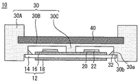
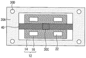
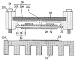
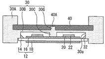
図1は、本発明の実施の形態1に係る半導体装置10の断面図である。半導体装置10は絶縁基板12を備えている。絶縁基板12は、セラミック基板14、セラミック基板14の上面側に形成された金属パターン16、及びセラミック基板14の下面側に形成された金属膜18を備えている。金属パターン16と金属膜18は例えばアルミで形成されている。このように、絶縁基板12は、セラミック基板14の両面にアルミを形成した構成である。
図5は、本発明の実施の形態2に係る半導体装置の断面図である。この半導体装置は、押さえ部30Eと押さえ部30Fを備えている。押さえ部30Eと押さえ部30Fが絶縁基板12に接することで、絶縁基板12が上に凸に反ることを防止する。このように、押さえ部を複数備えることで絶縁基板12が上に凸に反ることを確実に防止できる。
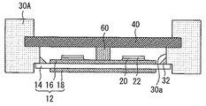
図6は、本発明の実施の形態3に係る半導体装置の断面図である。押さえ部60は、例えばゴムなどの弾性体で形成されている。押さえ部60はケース30とは別部材である。押さえ部60により絶縁基板12が上に凸に反ることを抑制できる。また、絶縁基板12を上に凸に反らせる力が非常に強い場合、押さえ部により絶縁基板の変位を完全に防止してしまうと、絶縁基板のクラックの原因となる。しかし、弾性体により絶縁基板の僅かな反りを許容することで、クラックを防止できる。
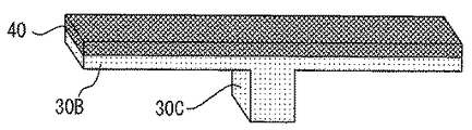
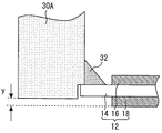
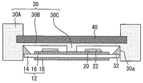
図7は、本発明の実施の形態4に係る半導体装置の断面図である。絶縁基板12は、押さえ部30Cにより下方に押圧されることで下に凸に反っている。また、絶縁基板12の下面はケース30の下面よりも下に位置している。
図10は、本発明の実施の形態5に係る半導体装置の断面図である。金属支持体40は凹部40Aを有している。そして、凹部40Aはケース30の樹脂30Gで満たされている。樹脂30Gはインサート成形で形成できる。凹部40Aに樹脂30Gを満たすことで、金属支持体40とケース30の接合面積を増やすことができるので、押さえ部30Cの剛性を高めることができる。よって、絶縁基板12が上に凸に反ることを確実に防止できる。
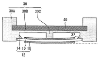
図11は、本発明の実施の形態6に係る半導体装置の断面図である。絶縁基板12は接着剤32のみを介して包囲部30Aと接している。そのため、絶縁基板12と包囲部30Aは直接接触していない。絶縁基板12の外周部がケース30よりもヤング率の小さい接着剤32のみと接することで、絶縁基板12の変位の応力が緩和され絶縁基板12が割れにくくなる。
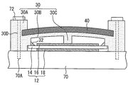
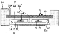
図12は、本発明の実施の形態7に係る半導体装置の断面図である。この半導体装置は、金属支持体40に接続された電極80を備えている。また、金属支持体40と電極80を同一部材で形成しても良い。そして、金属支持体40はワイヤ82、84により半導体素子22に接続されている。そのため、金属支持体40は、押さえ部30Cを固定する機能に加えて、半導体素子22の電極としての機能も有する。従って、半導体装置内における部品の実装密度を高め半導体装置内部の空間を効率的に利用できる。これは、半導体装置の小型化に寄与する。
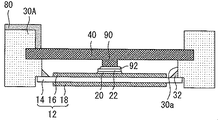
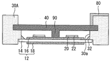
図13は、本発明の実施の形態8に係る半導体装置の断面図である。押さえ部90は金属支持体40と一体的に金属で形成されている。そして、押さえ部90は、はんだ92により半導体素子22の電極に固定されている。従って、電極80と半導体素子22をワイヤなどで接続する必要がないので、製造コストを低減できる。なお、更に製造コストを低減するために、電極80、金属支持体40、及び押さえ部90を一体的に金属で形成しても良い。
図14は、本発明の実施の形態9に係る半導体装置の断面図である。押さえ部90は金属支持体40と一体的に金属で形成されている。そして、押さえ部90は、半導体素子22の裏面電極と電気的に接続された金属パターン16に固定されている。押さえ部90の応力、絶縁基板12が上に凸に反ろうとする力、又はこれら両方の力により、はんだを用いることなく、押さえ部90と金属パターン16が接触している。押さえ部90と金属パターン16の固定を確実にするためにはんだを用いてもよい。
Claims (8)
- 絶縁基板と、
前記絶縁基板の上面に固定された半導体素子と、
前記半導体素子を囲む包囲部を有する、樹脂で形成されたケースと、
端部が前記包囲部に固定され、前記絶縁基板の上に位置する金属支持体と、
前記絶縁基板が上に凸に反らないように、前記金属支持体から下方に伸びる押さえ部と、
前記絶縁基板と前記ケースを接着する接着剤と、を備え、
前記絶縁基板は、前記金属支持体の復元力が付与された前記押さえ部により下方に押圧されることで下に凸に反り、
前記絶縁基板の下面は前記ケースの下面よりも下に位置することを特徴とする半導体装置。 - 前記押さえ部を複数備えたことを特徴とする請求項1に記載の半導体装置。
- 前記押さえ部を弾性体で形成したことを特徴とする請求項1に記載の半導体装置。
- 前記金属支持体は銅で形成され、
前記樹脂はPPS樹脂であることを特徴とする請求項1〜3のいずれか1項に記載の半導体装置。 - 前記絶縁基板は前記接着剤のみを介して前記包囲部と接したことを特徴とする請求項1〜4のいずれか1項に記載の半導体装置。
- 前記絶縁基板は、セラミック基板の両面にアルミを形成した構成であることを特徴とする請求項1〜5のいずれか1項に記載の半導体装置。
- 前記半導体素子は、ワイドバンドギャップ半導体によって形成されたことを特徴とする請求項1〜6のいずれか1項に記載の半導体装置。
- 前記ワイドバンドギャップ半導体は、炭化珪素、窒化ガリウム系材料、又はダイヤモンドであることを特徴とする請求項7に記載の半導体装置。
Priority Applications (4)
| Application Number | Priority Date | Filing Date | Title |
|---|---|---|---|
| JP2013226712A JP6480098B2 (ja) | 2013-10-31 | 2013-10-31 | 半導体装置 |
| US14/296,778 US9633918B2 (en) | 2013-10-31 | 2014-06-05 | Semiconductor device |
| DE102014217266.7A DE102014217266B4 (de) | 2013-10-31 | 2014-08-29 | Halbleitervorrichtung |
| CN201410475125.XA CN104600038B (zh) | 2013-10-31 | 2014-09-17 | 半导体装置 |
Applications Claiming Priority (1)
| Application Number | Priority Date | Filing Date | Title |
|---|---|---|---|
| JP2013226712A JP6480098B2 (ja) | 2013-10-31 | 2013-10-31 | 半導体装置 |
Related Child Applications (1)
| Application Number | Title | Priority Date | Filing Date |
|---|---|---|---|
| JP2017196550A Division JP6421859B2 (ja) | 2017-10-10 | 2017-10-10 | 半導体装置 |
Publications (2)
| Publication Number | Publication Date |
|---|---|
| JP2015088653A JP2015088653A (ja) | 2015-05-07 |
| JP6480098B2 true JP6480098B2 (ja) | 2019-03-06 |
Family
ID=52811967
Family Applications (1)
| Application Number | Title | Priority Date | Filing Date |
|---|---|---|---|
| JP2013226712A Active JP6480098B2 (ja) | 2013-10-31 | 2013-10-31 | 半導体装置 |
Country Status (4)
| Country | Link |
|---|---|
| US (1) | US9633918B2 (ja) |
| JP (1) | JP6480098B2 (ja) |
| CN (1) | CN104600038B (ja) |
| DE (1) | DE102014217266B4 (ja) |
Families Citing this family (7)
| Publication number | Priority date | Publication date | Assignee | Title |
|---|---|---|---|---|
| US10510642B2 (en) * | 2016-06-03 | 2019-12-17 | Mitsubishi Electric Corporation | Semiconductor device module |
| EP3340291B1 (en) * | 2016-12-23 | 2024-10-30 | Infineon Technologies AG | Method for producing an electronic module assembly and electronic module assembly |
| JP7006706B2 (ja) * | 2018-01-05 | 2022-01-24 | 三菱電機株式会社 | 半導体装置 |
| JP7006812B2 (ja) * | 2018-12-10 | 2022-01-24 | 富士電機株式会社 | 半導体装置 |
| DE112020007724T5 (de) * | 2020-10-23 | 2023-08-10 | Mitsubishi Electric Corporation | Halbleitervorrichtung und Verfahren zur Fertigung der Halbleitervorrichtung |
| JP2023031825A (ja) | 2021-08-25 | 2023-03-09 | 富士電機株式会社 | 半導体装置及び半導体装置の製造方法 |
| JP7794027B2 (ja) * | 2022-03-04 | 2026-01-06 | 富士電機株式会社 | 半導体装置の製造方法 |
Family Cites Families (19)
| Publication number | Priority date | Publication date | Assignee | Title |
|---|---|---|---|---|
| JP3316714B2 (ja) | 1994-05-31 | 2002-08-19 | 三菱電機株式会社 | 半導体装置 |
| DE19530264A1 (de) | 1995-08-17 | 1997-02-20 | Abb Management Ag | Leistungshalbleitermodul |
| US6218730B1 (en) * | 1999-01-06 | 2001-04-17 | International Business Machines Corporation | Apparatus for controlling thermal interface gap distance |
| JP3519299B2 (ja) * | 1999-01-06 | 2004-04-12 | 芝府エンジニアリング株式会社 | 半導体装置 |
| JP2003303933A (ja) * | 2002-04-12 | 2003-10-24 | Toyota Motor Corp | 半導体装置の製造方法 |
| JP2004179584A (ja) * | 2002-11-29 | 2004-06-24 | Toyo Jushi Kk | トランジスタパッケージ及びその製造方法 |
| DE102006006425B4 (de) | 2006-02-13 | 2009-06-10 | Semikron Elektronik Gmbh & Co. Kg | Leistungshalbleitermodul in Druckkontaktausführung |
| JP2008244394A (ja) * | 2007-03-29 | 2008-10-09 | Sumitomo Electric Ind Ltd | 半導体装置 |
| DE102008051560A1 (de) | 2007-10-18 | 2009-04-23 | Infineon Technologies Ag | Leistungshalbleitermodul |
| US7944033B2 (en) * | 2007-10-18 | 2011-05-17 | Infineon Technologies Ag | Power semiconductor module |
| US7851267B2 (en) | 2007-10-18 | 2010-12-14 | Infineon Technologies Ag | Power semiconductor module method |
| DE102009002191B4 (de) * | 2009-04-03 | 2012-07-12 | Infineon Technologies Ag | Leistungshalbleitermodul, Leistungshalbleitermodulanordnung und Verfahren zur Herstellung einer Leistungshalbleitermodulanordnung |
| DE102009026558B3 (de) | 2009-05-28 | 2010-12-02 | Infineon Technologies Ag | Leistungshalbleitermodul mit beweglich gelagerten Schaltungsträgern und Verfahren zur Herstellung eines solchen Leistungshalbleitermoduls |
| DE102009046258B3 (de) * | 2009-10-30 | 2011-07-07 | Infineon Technologies AG, 85579 | Leistungshalbleitermodul und Verfahren zum Betrieb eines Leistungshalbleitermoduls |
| JP5450192B2 (ja) * | 2010-03-24 | 2014-03-26 | 日立オートモティブシステムズ株式会社 | パワーモジュールとその製造方法 |
| WO2011136070A1 (ja) * | 2010-04-27 | 2011-11-03 | 京セラ株式会社 | 弾性波装置およびその製造方法 |
| DE102010041892A1 (de) | 2010-10-01 | 2012-04-05 | Semikron Elektronik Gmbh & Co. Kg | Leistungshalbleitermodul mit einem Grundmodul und einem Verbindungsmodul |
| JP5669657B2 (ja) * | 2011-04-11 | 2015-02-12 | 三菱電機株式会社 | 半導体装置 |
| JP5665729B2 (ja) * | 2011-12-27 | 2015-02-04 | 三菱電機株式会社 | 電力用半導体装置 |
-
2013
- 2013-10-31 JP JP2013226712A patent/JP6480098B2/ja active Active
-
2014
- 2014-06-05 US US14/296,778 patent/US9633918B2/en active Active
- 2014-08-29 DE DE102014217266.7A patent/DE102014217266B4/de active Active
- 2014-09-17 CN CN201410475125.XA patent/CN104600038B/zh active Active
Also Published As
| Publication number | Publication date |
|---|---|
| CN104600038B (zh) | 2017-07-18 |
| CN104600038A (zh) | 2015-05-06 |
| US9633918B2 (en) | 2017-04-25 |
| DE102014217266A1 (de) | 2015-04-30 |
| JP2015088653A (ja) | 2015-05-07 |
| US20150115282A1 (en) | 2015-04-30 |
| DE102014217266B4 (de) | 2023-11-16 |
Similar Documents
| Publication | Publication Date | Title |
|---|---|---|
| JP6480098B2 (ja) | 半導体装置 | |
| JP6323325B2 (ja) | 半導体装置、半導体装置の製造方法 | |
| JP6526323B2 (ja) | パワーモジュール、パワー半導体装置及びパワーモジュール製造方法 | |
| JP6743916B2 (ja) | 半導体装置及び半導体装置の製造方法 | |
| JP6768612B2 (ja) | 半導体装置 | |
| JP6421859B2 (ja) | 半導体装置 | |
| JP6813259B2 (ja) | 半導体装置 | |
| JP6548146B2 (ja) | 回路構成体 | |
| JP7247574B2 (ja) | 半導体装置 | |
| JP6391527B2 (ja) | パワー半導体モジュール | |
| JP6907670B2 (ja) | 半導体装置および半導体装置の製造方法 | |
| JP2010050395A (ja) | 半導体装置およびその製造方法 | |
| JP6364556B1 (ja) | 電子装置 | |
| JP2015090965A (ja) | 半導体装置 | |
| JP2016054249A (ja) | 半導体装置 | |
| JP6702431B2 (ja) | 半導体装置 | |
| JP4046623B2 (ja) | パワー半導体モジュールおよびその固定方法 | |
| JP5693395B2 (ja) | 半導体装置 | |
| JP6080929B2 (ja) | 半導体モジュール | |
| JP3191112U (ja) | 半導体装置及び半導体装置用ケース | |
| JP6771581B2 (ja) | 半導体モジュール及び半導体装置 | |
| JP5124329B2 (ja) | 半導体装置 | |
| JP5062189B2 (ja) | 半導体装置の実装構造 | |
| JP4994025B2 (ja) | 樹脂封止型電子機器 | |
| JP2014093342A (ja) | 絶縁基板および半導体装置 |
Legal Events
| Date | Code | Title | Description |
|---|---|---|---|
| A621 | Written request for application examination |
Free format text: JAPANESE INTERMEDIATE CODE: A621 Effective date: 20151217 |
|
| A131 | Notification of reasons for refusal |
Free format text: JAPANESE INTERMEDIATE CODE: A131 Effective date: 20161004 |
|
| A521 | Request for written amendment filed |
Free format text: JAPANESE INTERMEDIATE CODE: A523 Effective date: 20161026 |
|
| A131 | Notification of reasons for refusal |
Free format text: JAPANESE INTERMEDIATE CODE: A131 Effective date: 20170207 |
|
| A521 | Request for written amendment filed |
Free format text: JAPANESE INTERMEDIATE CODE: A523 Effective date: 20170309 |
|
| A02 | Decision of refusal |
Free format text: JAPANESE INTERMEDIATE CODE: A02 Effective date: 20170725 |
|
| A521 | Request for written amendment filed |
Free format text: JAPANESE INTERMEDIATE CODE: A523 Effective date: 20171010 |
|
| A911 | Transfer to examiner for re-examination before appeal (zenchi) |
Free format text: JAPANESE INTERMEDIATE CODE: A911 Effective date: 20171019 |
|
| A912 | Re-examination (zenchi) completed and case transferred to appeal board |
Free format text: JAPANESE INTERMEDIATE CODE: A912 Effective date: 20171215 |
|
| A521 | Request for written amendment filed |
Free format text: JAPANESE INTERMEDIATE CODE: A523 Effective date: 20181130 |
|
| A61 | First payment of annual fees (during grant procedure) |
Free format text: JAPANESE INTERMEDIATE CODE: A61 Effective date: 20190207 |
|
| R150 | Certificate of patent or registration of utility model |
Ref document number: 6480098 Country of ref document: JP Free format text: JAPANESE INTERMEDIATE CODE: R150 |
|
| R250 | Receipt of annual fees |
Free format text: JAPANESE INTERMEDIATE CODE: R250 |
|
| R250 | Receipt of annual fees |
Free format text: JAPANESE INTERMEDIATE CODE: R250 |
|
| R250 | Receipt of annual fees |
Free format text: JAPANESE INTERMEDIATE CODE: R250 |
|
| R250 | Receipt of annual fees |
Free format text: JAPANESE INTERMEDIATE CODE: R250 |
|
| R250 | Receipt of annual fees |
Free format text: JAPANESE INTERMEDIATE CODE: R250 |