EP0756244A2 - Unité électronique et procédé de fabrication de cette unité - Google Patents
Unité électronique et procédé de fabrication de cette unité Download PDFInfo
- Publication number
- EP0756244A2 EP0756244A2 EP96112037A EP96112037A EP0756244A2 EP 0756244 A2 EP0756244 A2 EP 0756244A2 EP 96112037 A EP96112037 A EP 96112037A EP 96112037 A EP96112037 A EP 96112037A EP 0756244 A2 EP0756244 A2 EP 0756244A2
- Authority
- EP
- European Patent Office
- Prior art keywords
- coil
- carrier substrate
- layers
- circuit unit
- layer
- Prior art date
- Legal status (The legal status is an assumption and is not a legal conclusion. Google has not performed a legal analysis and makes no representation as to the accuracy of the status listed.)
- Granted
Links
Images

Classifications
-
- G—PHYSICS
- G06—COMPUTING; CALCULATING OR COUNTING
- G06K—GRAPHICAL DATA READING; PRESENTATION OF DATA; RECORD CARRIERS; HANDLING RECORD CARRIERS
- G06K19/00—Record carriers for use with machines and with at least a part designed to carry digital markings
- G06K19/06—Record carriers for use with machines and with at least a part designed to carry digital markings characterised by the kind of the digital marking, e.g. shape, nature, code
- G06K19/067—Record carriers with conductive marks, printed circuits or semiconductor circuit elements, e.g. credit or identity cards also with resonating or responding marks without active components
- G06K19/07—Record carriers with conductive marks, printed circuits or semiconductor circuit elements, e.g. credit or identity cards also with resonating or responding marks without active components with integrated circuit chips
- G06K19/077—Constructional details, e.g. mounting of circuits in the carrier
- G06K19/07749—Constructional details, e.g. mounting of circuits in the carrier the record carrier being capable of non-contact communication, e.g. constructional details of the antenna of a non-contact smart card
- G06K19/0775—Constructional details, e.g. mounting of circuits in the carrier the record carrier being capable of non-contact communication, e.g. constructional details of the antenna of a non-contact smart card arrangements for connecting the integrated circuit to the antenna
-
- G—PHYSICS
- G06—COMPUTING; CALCULATING OR COUNTING
- G06K—GRAPHICAL DATA READING; PRESENTATION OF DATA; RECORD CARRIERS; HANDLING RECORD CARRIERS
- G06K19/00—Record carriers for use with machines and with at least a part designed to carry digital markings
- G06K19/06—Record carriers for use with machines and with at least a part designed to carry digital markings characterised by the kind of the digital marking, e.g. shape, nature, code
- G06K19/067—Record carriers with conductive marks, printed circuits or semiconductor circuit elements, e.g. credit or identity cards also with resonating or responding marks without active components
- G06K19/07—Record carriers with conductive marks, printed circuits or semiconductor circuit elements, e.g. credit or identity cards also with resonating or responding marks without active components with integrated circuit chips
- G06K19/077—Constructional details, e.g. mounting of circuits in the carrier
- G06K19/07749—Constructional details, e.g. mounting of circuits in the carrier the record carrier being capable of non-contact communication, e.g. constructional details of the antenna of a non-contact smart card
- G06K19/07773—Antenna details
- G06K19/07777—Antenna details the antenna being of the inductive type
- G06K19/07779—Antenna details the antenna being of the inductive type the inductive antenna being a coil
- G06K19/07783—Antenna details the antenna being of the inductive type the inductive antenna being a coil the coil being planar
-
- G—PHYSICS
- G06—COMPUTING; CALCULATING OR COUNTING
- G06K—GRAPHICAL DATA READING; PRESENTATION OF DATA; RECORD CARRIERS; HANDLING RECORD CARRIERS
- G06K19/00—Record carriers for use with machines and with at least a part designed to carry digital markings
- G06K19/06—Record carriers for use with machines and with at least a part designed to carry digital markings characterised by the kind of the digital marking, e.g. shape, nature, code
- G06K19/067—Record carriers with conductive marks, printed circuits or semiconductor circuit elements, e.g. credit or identity cards also with resonating or responding marks without active components
- G06K19/07—Record carriers with conductive marks, printed circuits or semiconductor circuit elements, e.g. credit or identity cards also with resonating or responding marks without active components with integrated circuit chips
- G06K19/077—Constructional details, e.g. mounting of circuits in the carrier
- G06K19/07749—Constructional details, e.g. mounting of circuits in the carrier the record carrier being capable of non-contact communication, e.g. constructional details of the antenna of a non-contact smart card
- G06K19/07773—Antenna details
- G06K19/07777—Antenna details the antenna being of the inductive type
- G06K19/07784—Antenna details the antenna being of the inductive type the inductive antenna consisting of a plurality of coils stacked on top of one another
-
- H—ELECTRICITY
- H01—ELECTRIC ELEMENTS
- H01L—SEMICONDUCTOR DEVICES NOT COVERED BY CLASS H10
- H01L2224/00—Indexing scheme for arrangements for connecting or disconnecting semiconductor or solid-state bodies and methods related thereto as covered by H01L24/00
- H01L2224/01—Means for bonding being attached to, or being formed on, the surface to be connected, e.g. chip-to-package, die-attach, "first-level" interconnects; Manufacturing methods related thereto
- H01L2224/42—Wire connectors; Manufacturing methods related thereto
- H01L2224/47—Structure, shape, material or disposition of the wire connectors after the connecting process
- H01L2224/48—Structure, shape, material or disposition of the wire connectors after the connecting process of an individual wire connector
- H01L2224/4805—Shape
- H01L2224/4809—Loop shape
- H01L2224/48091—Arched
-
- H—ELECTRICITY
- H01—ELECTRIC ELEMENTS
- H01L—SEMICONDUCTOR DEVICES NOT COVERED BY CLASS H10
- H01L2224/00—Indexing scheme for arrangements for connecting or disconnecting semiconductor or solid-state bodies and methods related thereto as covered by H01L24/00
- H01L2224/01—Means for bonding being attached to, or being formed on, the surface to be connected, e.g. chip-to-package, die-attach, "first-level" interconnects; Manufacturing methods related thereto
- H01L2224/42—Wire connectors; Manufacturing methods related thereto
- H01L2224/47—Structure, shape, material or disposition of the wire connectors after the connecting process
- H01L2224/48—Structure, shape, material or disposition of the wire connectors after the connecting process of an individual wire connector
- H01L2224/481—Disposition
- H01L2224/48151—Connecting between a semiconductor or solid-state body and an item not being a semiconductor or solid-state body, e.g. chip-to-substrate, chip-to-passive
- H01L2224/48221—Connecting between a semiconductor or solid-state body and an item not being a semiconductor or solid-state body, e.g. chip-to-substrate, chip-to-passive the body and the item being stacked
- H01L2224/48225—Connecting between a semiconductor or solid-state body and an item not being a semiconductor or solid-state body, e.g. chip-to-substrate, chip-to-passive the body and the item being stacked the item being non-metallic, e.g. insulating substrate with or without metallisation
- H01L2224/48227—Connecting between a semiconductor or solid-state body and an item not being a semiconductor or solid-state body, e.g. chip-to-substrate, chip-to-passive the body and the item being stacked the item being non-metallic, e.g. insulating substrate with or without metallisation connecting the wire to a bond pad of the item
-
- Y—GENERAL TAGGING OF NEW TECHNOLOGICAL DEVELOPMENTS; GENERAL TAGGING OF CROSS-SECTIONAL TECHNOLOGIES SPANNING OVER SEVERAL SECTIONS OF THE IPC; TECHNICAL SUBJECTS COVERED BY FORMER USPC CROSS-REFERENCE ART COLLECTIONS [XRACs] AND DIGESTS
- Y10—TECHNICAL SUBJECTS COVERED BY FORMER USPC
- Y10T—TECHNICAL SUBJECTS COVERED BY FORMER US CLASSIFICATION
- Y10T29/00—Metal working
- Y10T29/49—Method of mechanical manufacture
- Y10T29/49002—Electrical device making
- Y10T29/4902—Electromagnet, transformer or inductor
- Y10T29/49073—Electromagnet, transformer or inductor by assembling coil and core
-
- Y—GENERAL TAGGING OF NEW TECHNOLOGICAL DEVELOPMENTS; GENERAL TAGGING OF CROSS-SECTIONAL TECHNOLOGIES SPANNING OVER SEVERAL SECTIONS OF THE IPC; TECHNICAL SUBJECTS COVERED BY FORMER USPC CROSS-REFERENCE ART COLLECTIONS [XRACs] AND DIGESTS
- Y10—TECHNICAL SUBJECTS COVERED BY FORMER USPC
- Y10T—TECHNICAL SUBJECTS COVERED BY FORMER US CLASSIFICATION
- Y10T29/00—Metal working
- Y10T29/49—Method of mechanical manufacture
- Y10T29/49002—Electrical device making
- Y10T29/49117—Conductor or circuit manufacturing
- Y10T29/49124—On flat or curved insulated base, e.g., printed circuit, etc.
- Y10T29/49155—Manufacturing circuit on or in base
- Y10T29/49165—Manufacturing circuit on or in base by forming conductive walled aperture in base
Definitions
- the invention relates to a circuit unit which comprises at least one insulating carrier substrate, on which a conductive coil is located, and an integrated circuit, the connection points of which are conductively connected to the coil ends.
- the invention further relates to a method for producing such a circuit unit.
- Circuit units of the above-mentioned type are already known from the prior art and are designed, for example, as a compact electronic module which is inserted into a chip card for contactless data exchange with a terminal.
- a circuit unit in the form of an electronic module with an insulating carrier substrate is known, on which an annular wound coil is glued.
- the coil ends are guided into the receiving space created by the ring-shaped coil, where they are conductively connected to the connection points of an integrated circuit.
- the receiving space for the integrated circuit and the coil ends is cast with a casting compound to protect these sensitive components from mechanical loads.
- the electronic module known from US Pat. No. 4,999,742 has a compact structure, but the coil has to be wound in a separate process step and glued to the insulating carrier substrate in a further process step.
- a circuit unit in the form of a chip card is known from the as yet unpublished German patent application P 44 16 697.4, a coil on one of the card layers of the multi-layer card body is printed from a conductive varnish, the coil ends are conductively connected to the connection points of an integrated circuit.
- the structure of the circuit unit known from patent application 44 16 697.4 has the advantage that the coil is printed directly onto a card layer and thus the process step of applying a separately manufactured coil to an insulating carrier substrate is omitted.
- the coil it is desirable that the coil have a higher number of coil turns than can be realized with the construction explained above.
- the manufacturing process of the circuit unit should be further optimized with a view to inexpensive mass production.
- An advantage of the invention is the fact that a higher number of turns can be realized than on the structure known from German patent application 44 16 197.4.
- the coil can continue to be applied directly to the carrier substrate of the circuit unit, so that an additional process step for the application of a separately manufactured coil is not required.
- This is made possible by the fact that coil layers and insulating layers are alternately applied to the insulating carrier substrate, the individual coil layers being conductively connected to one another via plated-through holes, so that a coil is formed.
- the coil layers and the insulating layers are preferably printed on. Alternatively, it is also possible for the insulating layers to consist of thin insulating foils on which the coil layers are printed on one or both sides.
- the through-plating through the insulating layers can take place by providing windows or holes in the insulating layers through which the conductive material of the coil layers penetrates when the coil layers are printed on or when the layers are laminated together.
- additional conductive material can also be applied for the plated-through hole or additional conductive elements can be provided.
- circuit unit can be manufactured particularly easily using the multiple-use process, since when applying the coil layers and, depending on the embodiment, also the insulating layers, the printing technology can be used in which multiple-use production is common .
- the invention has the advantage that the coil ends can be adapted in a particularly simple manner to the different possibilities of establishing the conductive connection between the coil ends and the connection points of the integrated circuit.
- the invention permits the embossing of the circuit unit without restriction, without the risk of interruption of one or more coil turns.
- the Coil turns are outside the embossed area of the circuit unit or between the individual embossed lines, whereby the width of the coil turns to compensate for manufacturing tolerances can be greater than the line spacing or the coil turns are in the area of the embossed characters, but are wider than the character size.
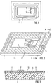
- the circuit unit contains an insulating carrier substrate 1 in the form of a card layer on which the coil 3 lies, the coil ends 15 and 19 of which are conductively connected to the connection points of an integrated circuit 7.
- the integrated circuit can also be cast into a module which, for easier contacting of the integrated circuit 7, has contact surfaces which are conductively connected to the connection points of the integrated circuit 7.
- the coil turns of the coil 3 run along the outer edge of the card layer, so that a large-area coil is created in favor of high energy coupling.
- FIG. 2 shows a circuit unit according to the invention which is not to scale and in a perspective view and which is produced as described below.
- a first coil layer 9 which is shown in broken lines in FIG. 2 and can contain several coil turns, is first applied (the coil layer 9 shown contains, in order to keep the drawing clearer, only a coil turn).
- the coil layer 9 is preferably printed with a conductive lacquer, but it is also possible to spray the coil layer on using a corresponding mask or to etch it out from a conductive coating which is located on the carrier substrate. Other manufacturing techniques are conceivable.
- an insulating layer 11 is applied to the insulating carrier substrate 1, which is shown hatched in FIG. 2 and covers the coil turns of the coil layer 9.
- the isolating Layer 11 has a window 13 and is applied to the coil layer 9 such that the coil end 15 of the coil layer 9 is not covered by it and that at least the coil end of the last coil turn of the coil layer 9 is accessible through the window 13.
- the insulating layer 11 is preferably also printed, but here too it is possible to spray it on using an appropriate mask or to use a thin insulating film as the insulating layer 11, etc.
- a further coil layer 17 is applied to the insulating layer 11, for which purpose the same techniques are used as for the application of the coil layer 9.
- the further coil layer 17 is preferably also printed on.
- the coil layer 17 is conductively connected to the coil layer 9 through the window 13 in the insulating layer 11, so that a coil 3 consisting of the coil layers 9 and 17 is formed.
- the establishment of a conductive connection between the coil layers 9 and 17 can be facilitated in that the coil ends, which are conductively connected to one another, are widened with respect to the coil turns, as is also shown in FIG. 2. Such a broadening is easy to implement in terms of printing technology. Details of the connection technology are described below.
- the coil end 19 of the last applied coil layer is applied in such a way that the production of a conductive connection from the coil ends 15 and 19 to the integrated circuit 7 is particularly simple.
- the coil layers and the insulating layers are applied to the insulating carrier substrate 1 in a kind of frame.
- the coil ends 15 and 19 are guided into the interior of the frame on the insulating carrier substrate 1.
- a superposition of coil turns in a coil layer is avoided in that the inner coil end of the respective coil layer is guided into the part enclosed by the frame, as is also shown in FIG. 2.
- a suitable choice of the coil ends, which are conductively connected to the integrated circuit, can always avoid overlapping of coil turns in a coil position. For example, if the coil end 19 is to be outside the frame, the inner coil end of the coil layer 17 is connected to the coil layer 9 and the outer coil end of the coil layer 17 is guided to the outside.
- an insulating layer with a window to the last coil layer, the free coil end of which is connected to the integrated circuit.
- the free end of the coil can then be guided through the window in any direction over the layer of coils, since there can be no short circuit between the coil turns due to the covering layer.
- the integrated circuit 7 is applied to the uncovered part of the insulating carrier substrate 1, the connection points of which are e.g. can be conductively connected to the coil ends 15 and 19 of the resulting coil by means of bonding wires 21.
- the production of the conductive connections from the integrated circuit 7 to the coil ends 15 and 19 can be simplified by making the coil ends wider than the individual coil turns.
- the printing templates or, in the case of sprayed-on coil layers, the masks used only need to be adapted accordingly. Separate process steps for producing widened coil ends are therefore not necessary.
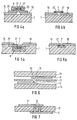
- FIG. 3 shows a cross section along the line A - A of FIG. 2 in order to clarify the layer sequence.
- the coil layer 9 is applied to the insulating carrier substrate 1 and is covered by the insulating layer 11, which contains a window 13 through which the further coil layer 17 is conductively connected to the coil layer 9.
- Other insulating layers and coil layers can alternate.
- connection between the integrated circuit 7 and the coil ends 15 and 19 is not established via bonding wires, but rather by placing the integrated circuit 7 directly on the coil ends 15 and 19.
- the integrated circuit 7 or a module 23 the contains the integrated circuit 7, either be placed on the already applied coil ends 15 and 19 or the Circuit 7 or module 23 is first inserted into carrier substrate 1 and then overprinted with coil ends 15 and 19.
- Fig. 4 shows cross sections of two embodiments of the circuit unit according to the invention, in which the coil ends 15 and 19 were first printed on the carrier substrate 1 and then the module 23 or the integrated circuit 7 is placed on the coil ends 15 and 19.
- the module 23 or the integrated circuit 7 can optionally be put on immediately after the printing process or only after a short period in which the printed conductive lacquer dries at least partially.
- FIG. 4a shows the carrier substrate 1 with printed coil ends 15 and 19 and the module 23.
- the module 23 contains the integrated circuit 7, which is encased in a sealing compound 8 and the connection points 27 of which are conductively connected to contacts 25 of the module 23 via bonding wires.
- the module 23 is placed on the coil ends 15 and 19 such that the contacts 25 of the module 23 touch the coil ends 15 and 19, respectively.
- the arrangement shown in FIG. 4a can be covered by a cover film, not shown in the figure, which may contain a recess for the module 23.
- the module 23 is placed on the coil ends 15 and 19 so that the sealing compound 8 points away from the coil ends 15 and 19.
- a corresponding recess is to be provided in the carrier substrate 1, which partially accommodates the sealing compound 8. This variant is used in particular when a low overall height of the circuit unit is to be achieved.
- FIG. 4b again shows a carrier substrate 1 with printed coil ends 15 and 19.
- the integrated circuit 7 is placed on the coil ends 15 and 19 such that the connection points 27 of the integrated circuit 7 touch the coil ends 15 and 19, respectively.
- the structure shown in FIG. 4b can also be protected by a cover film, not shown, which can optionally contain a cutout for the integrated circuit 7.
- FIG. 5 shows cross sections of two embodiments of the circuit unit according to the invention, in which the module 23 or the integrated circuit 7 is overprinted for contacting the coil ends 15 and 19.
- the module 23 is fitted into the carrier substrate 1 such that the surface of the module 23 is flush with the surface of the carrier substrate 1.
- the printed after the insertion of the module 23 in the carrier substrate 1 coil ends 15 and 19 extend so far over the surface of the module 23 that they partially cover the contacts 25 of the module 23, so that a conductive connection between the contacts 25 and the coil ends 15 and 19 arises.
- the integrated circuit 7 is inserted into the carrier substrate 1 such that the surface of the integrated circuit 7 is flush with the surface of the carrier substrate 1 and the connection points 27 of the integrated circuit 7 point upwards.
- the coil ends 15 and 19 are printed on the carrier substrate 1 in such a way that they extend beyond the connection points 27 of the integrated circuit 7. In this way, a conductive connection is established between the connection points 27 and the coil ends 15 and 19.
- To embed the integrated circuit 7 in the carrier substrate 1 can either a corresponding recess is provided or the chip can be pressed into the carrier substrate 1 using heat and pressure.
- FIG. 6 shows an embodiment of the circuit unit according to the invention in cross section, in which the through-plating takes place when the individual layers of the circuit unit are laminated together. The layer sequence of the circuit unit before the lamination process is shown.
- a carrier substrate 1a with a coil layer 17 and a carrier substrate 1b with a coil layer 9 are separated from one another by an insulating film 11.
- a window 13 is made in the film 11 by punching out, piercing or by means of a laser beam at a point at which the coil layers 9 and 17 face each other.
- a laminate is produced from the individual layers 1a, 1b and 11 by lamination.
- the lamination process ensures that an electrically conductive connection between the coil layer 9 and the coil layer 17 is created through the window 13. This can be further supported by applying a small portion of conductive adhesive 29 to at least one of the coil layers 9 and 17 opposite the window 13, which flows into the window 13 during lamination and thus creates an electrically conductive connection between the coil layers 9 and 17.
- Fig. 7 shows an embodiment of the circuit unit according to the invention in cross section, in which the insulating film 11 is printed on both sides with coil layers 9 and 17, the coil layers 9 and 17 partially overlap.
- the insulating film 11 has one or more windows 13, which are produced, for example, by punching, piercing or by means of a laser beam. These windows 13 are filled with the printing material, for example a conductive varnish, when the coil layers 9 and 17 are screen printed onto the insulating film 11 and thus establish one or more conductive connections between the coil layers 9 and 17.
- FIG. 8 shows a further exemplary embodiment for the plated-through hole.
- coil layers 9 and 17 are applied on the opposite sides of the insulating film so that they partially overlap.
- at least one thin wire 31 is shot in, which pierces the coil layer 17, the insulating film 11 and at least partially also the coil layer 9 and thus creates a conductive connection between the coil layers 9 and 17.
- the wire 31 can also be passed completely through the coil layer 9 and bent at its end by a suitable device. In order to facilitate the passage of the wire 31, it can be heated in a variant of the exemplary embodiment.
- FIG. 9 shows an exemplary embodiment in which the coil layers 9 and 17 are first applied to the opposite sides of the insulating film 11. Subsequently, in the area in which the opposing coil layers 9 and 17 overlap, at least one window 13 is introduced in the coil layers 9 and 17 and the insulating film 11 in between, for example by punching, piercing or by means of a laser beam. The window 13 is finally filled with a conductive adhesive 33 and thus a conductive connection between the coil layers 9 and 17 is made.
- FIG. 10 shows an exemplary embodiment in which a conductive connection between the coil layers 9 and 17 can be established by means of a connecting element 35.
- the 10a shows the layer sequence of the circuit unit before the lamination process.
- the coil layer 9 is applied to the carrier substrate 1.
- the insulating film 11 is arranged above the carrier substrate 1 and supports the coil layer 17 and has the window 13 in an area opposite the coil layer 9 and adjacent to the coil layer 17.
- the connecting element 35 is arranged on an auxiliary carrier film 37 above the window 13 and overlapping with the coil layer 17.
- the connecting element 35 can consist, for example, of a thermally activatable conductive adhesive.
- FIG. 10b shows the layer structure from FIG. 10a after lamination.
- the in-Fig. 10a layers can be joined together by means of a conventional laminating press under pressure and heat to form a composite.
- the stamp of the laminating press pressing against the top of the structure is shaped in such a way that the connecting element 35 is pressed through the window 13 against the coil layer 9 during the laminating process and connects to it.
- the other end of the connecting element 35 is pressed against the coil layer 17 and connects to it. In this way, a conductive connection between the coil layers 9 and 17 is established.
- the auxiliary carrier film 37 detaches from the connecting element 35 during the lamination process and is subsequently removed.
- the window or windows 13 in the insulating layer 11 can be omitted.
- the coil layers are capacitively coupled.
- the capacitive coupling can also be used for coupling the integrated circuit 7 to the coil 3, so that a conductive connection can also be omitted here.
- Another aspect of the invention consists in lifting previously existing restrictions regarding the high embossability of a circuit unit containing a coil 3. This can be done by various measures, which can be used both with single-layer and with multi-layer coils 3.
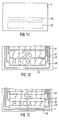
- FIG. 11 shows a top view of a circuit unit, areas 37 and 38 within which embossing is permitted for chip cards in accordance with ISO standard 7811 are each delimited by a dashed line.
- embossing for example, letters and numbers or other characters can be emphasized. If necessary, the embossed characters can be printed on a paper document using a suitable device.
- the embossing can damage the coil 3.
- the lower region 37 is particularly problematic with regard to possible damage to coil turns, since a large-area coil 3 is generally required, and the coil turns therefore run near the edge of the circuit unit.
- FIG. 12 shows an enlarged section of the circuit unit shown in FIG. 11 in a top view.
- a turn 39 between the embossing field 37 and the edge of the carrier substrate 1 arranged. If sufficient space is available, several turns or even all turns of the coil 3 can also run here. Since no embossing takes place in this area, there is also no risk that the turns of the coil 3 will be interrupted by the embossing process. With a multi-layer coil, the space becomes scarce only with higher numbers of turns than with a single-layer coil, since not all turns have to be arranged side by side.
- turns 41 which are so widened in this area that they are wider than the size of the characters embossed there. This ensures that the turns 41 are not interrupted by the embossing process, even if the embossed characters would each cut through a cross section of the turns 41 corresponding to the size of the characters. If there is not enough space for one or more turns 39 outside the high embossing field 37, all the turns 41 can also be guided through the high embossing field 37.
- FIG. 13 also shows an enlarged section of the circuit unit shown in FIG. 11 in a top view.
- the turns of the coil 3 are either guided between the high embossing field 37 and the edge of the circuit unit, turn 39, or following the high embossing lines or between the individual high embossing lines, turns 43.
- the turns 43, the run between the embossing lines or immediately after the embossing lines, are somewhat broadened to compensate for manufacturing tolerances. This ensures that at least a portion of these turns 43 runs on a surface that is not embossed and thus does not involve the risk of interruption of these turns 43 brings itself.
- FIG. 13 shows an enlarged section of the circuit unit shown in FIG. 11 in a top view.
- the properties of the coating material used to produce the windings can be matched as closely as possible to the carrier substrate 1 to which they are applied, so that the coating material does not tear and thus the windings are interrupted when embossed. It is also conceivable to use conductive plastics as coating material which are so elastic that they do not tear when embossed.
- the resistance of the coil 3 may assume inadmissibly high values, since the turns 39 must be very narrow due to the limited space available. This problem can be counteracted by applying the coils 39 in thicker layers, which can be achieved, for example, by multiple printing. Likewise, it is also possible to widen the windings 39 in the areas in which sufficient space is available in order to reduce the resistance.
- the circuit unit can be manufactured both in individual piece production and by means of arches or webs, which are each divided into individual circuit units at the end of production.
- the measures described to improve the circuit unit such as, for example, providing a multilayer coil structure, different through-connection variants being possible, enabling the circuit unit to be embossed by suitable selection of the dimensions and the course, possibly also the material of the coil layers, and direct contacting of the integrated circuit or Modules on the coil can be used individually or in combination.
Applications Claiming Priority (2)
| Application Number | Priority Date | Filing Date | Title |
|---|---|---|---|
| DE19527359 | 1995-07-26 | ||
| DE19527359A DE19527359A1 (de) | 1995-07-26 | 1995-07-26 | Schaltungseinheit und Verfahren zur Herstellung einer Schaltungseinheit |
Publications (3)
| Publication Number | Publication Date |
|---|---|
| EP0756244A2 true EP0756244A2 (fr) | 1997-01-29 |
| EP0756244A3 EP0756244A3 (fr) | 1998-12-09 |
| EP0756244B1 EP0756244B1 (fr) | 2003-03-12 |
Family
ID=7767864
Family Applications (1)
| Application Number | Title | Priority Date | Filing Date |
|---|---|---|---|
| EP96112037A Expired - Lifetime EP0756244B1 (fr) | 1995-07-26 | 1996-07-25 | Unité électronique et procédé de fabrication de cette unité |
Country Status (4)
| Country | Link |
|---|---|
| US (2) | US6049461A (fr) |
| EP (1) | EP0756244B1 (fr) |
| DE (2) | DE19527359A1 (fr) |
| ES (1) | ES2191073T3 (fr) |
Cited By (18)
| Publication number | Priority date | Publication date | Assignee | Title |
|---|---|---|---|---|
| DE19642378A1 (de) * | 1996-10-14 | 1998-04-16 | Fraunhofer Ges Forschung | Kontaktlose Chipkarte |
| DE19733348A1 (de) * | 1997-08-01 | 1998-09-03 | Siemens Ag | Kartenförmiger Datenträger mit einer Spule für eine kontaktlose Datenübertragung und Vorrichtung zum Wickeln einer solchen Spule |
| WO1998048378A2 (fr) * | 1997-04-21 | 1998-10-29 | Siemens Aktiengesellschaft | Revetement pour cartes a puce |
| WO1999003165A1 (fr) * | 1997-07-07 | 1999-01-21 | Siemens Aktiengesellschaft | Carte a puce et procede de mise en contact d'une antenne encastree dans une carte a puce |
| FR2769390A1 (fr) * | 1997-10-08 | 1999-04-09 | Gemplus Card Int | Procede de fabrication de cartes a puce aptes a assurer un fonctionnement a contact et sans contact, et de cartes a puce sans contact |
| WO2000021030A1 (fr) * | 1998-10-06 | 2000-04-13 | Intermec Ip Corp. | Transpondeur a identification de frequences radioelectriques a caracteristiques rf ameliorees |
| DE19840220A1 (de) * | 1998-09-03 | 2000-04-20 | Fraunhofer Ges Forschung | Transpondermodul und Verfahren zur Herstellung desselben |
| DE19847088A1 (de) * | 1998-10-13 | 2000-05-18 | Ksw Microtec Ges Fuer Angewand | Flächig ausgebildeter Träger für Halbleiter-Chips und Verfahren zu seiner Herstellung |
| WO2000043952A1 (fr) * | 1999-01-22 | 2000-07-27 | Intermec Ip Corp. | Transpondeur rfid |
| DE19940480A1 (de) * | 1999-08-26 | 2001-03-08 | Orga Kartensysteme Gmbh | Leiterbahnträgerschicht zur Einlaminierung in eine Chipkarte, Chipkarte mit einer Leiterbahnträgerschicht und Verfahren zur Herstellung einer Chipkarte |
| EP1107175A2 (fr) * | 1999-12-10 | 2001-06-13 | Sony Corporation | Carte à puce embossée et lecteur de cette carte |
| JP2002259920A (ja) * | 2001-02-27 | 2002-09-13 | Sony Corp | エンボス加工可能なicカード、その製造方法、エンボス付きicカード及びそれによる取引処理システム |
| EP1840802A1 (fr) * | 2006-03-30 | 2007-10-03 | Fujitsu Limited | Étiquette Rfid et procédé de fabrication correspondant |
| WO2011047835A1 (fr) | 2009-10-21 | 2011-04-28 | Giesecke & Devrient Gmbh | Fabrication de structures de conducteur sur des films en matière plastique au moyen de nano-encres |
| DE102010015659A1 (de) | 2010-04-20 | 2011-10-20 | Giesecke & Devrient Gmbh | Transferverfahren zur Herstellung von Leiterstrukturen mittels Nanotinten |
| DE102011016512A1 (de) * | 2011-04-08 | 2012-10-11 | Giesecke & Devrient Gmbh | Verfahren zur Durchkontaktierung elektrisch leitfähiger Strukturen an entgegengesetzten Oberflächen eines Substrats |
| DE102015014408A1 (de) * | 2015-11-06 | 2017-05-11 | Giesecke & Devrient Gmbh | Stabile Chipkarte, Spulenanordnung und Verfahren zum Bereitstellen einer Chipkarte |
| DE102009023848B4 (de) | 2009-06-04 | 2021-10-28 | Giesecke+Devrient Mobile Security Gmbh | Verfahren zur drucktechnischen Herstellung einer elektrischen Leiterbahn |
Families Citing this family (70)
| Publication number | Priority date | Publication date | Assignee | Title |
|---|---|---|---|---|
| USRE42773E1 (en) | 1992-06-17 | 2011-10-04 | Round Rock Research, Llc | Method of manufacturing an enclosed transceiver |
| US7158031B2 (en) * | 1992-08-12 | 2007-01-02 | Micron Technology, Inc. | Thin, flexible, RFID label and system for use |
| EP0824301A3 (fr) * | 1996-08-09 | 1999-08-11 | Hitachi, Ltd. | Panneau à circuit imprimé, carte à puce, et leur procédé de fabrication |
| DE19753619A1 (de) * | 1997-10-29 | 1999-05-06 | Meto International Gmbh | Identifizierungselement und Verfahren zu seiner Herstellung |
| DE19701167A1 (de) * | 1997-01-15 | 1998-07-23 | Siemens Ag | Chipkarte |
| US6329213B1 (en) * | 1997-05-01 | 2001-12-11 | Micron Technology, Inc. | Methods for forming integrated circuits within substrates |
| DE19728512A1 (de) * | 1997-07-04 | 1999-01-07 | Aeg Identifikationssys Gmbh | Transponderanordnung und Verfahren zu deren Herstellung |
| DE19730166A1 (de) * | 1997-07-14 | 1999-01-21 | Aeg Identifikationssys Gmbh | Transponderanordnung und Verfahren zu deren Herstellung |
| US6980085B1 (en) * | 1997-08-18 | 2005-12-27 | Micron Technology, Inc. | Wireless communication devices and methods of forming and operating the same |
| US6339385B1 (en) | 1997-08-20 | 2002-01-15 | Micron Technology, Inc. | Electronic communication devices, methods of forming electrical communication devices, and communication methods |
| FR2769389B1 (fr) * | 1997-10-07 | 2000-01-28 | Rue Cartes Et Systemes De | Carte a microcircuit combinant des plages de contact exterieur et une antenne, et procede de fabrication d'une telle carte |
| DE19745648A1 (de) * | 1997-10-15 | 1998-11-26 | Siemens Ag | Trägerelement für einen Halbleiterchip zum Einbau in Chipkarten |
| US6164551A (en) * | 1997-10-29 | 2000-12-26 | Meto International Gmbh | Radio frequency identification transponder having non-encapsulated IC chip |
| US6030423A (en) * | 1998-02-12 | 2000-02-29 | Micron Technology, Inc. | Thin profile battery bonding method and method of conductively interconnecting electronic components |
| US6252777B1 (en) * | 1998-02-13 | 2001-06-26 | Shinko Electric Industries Co., Ltd. | IC card and its frame |
| US6255725B1 (en) * | 1998-05-28 | 2001-07-03 | Shinko Electric Industries Co., Ltd. | IC card and plane coil for IC card |
| DE29814277U1 (de) * | 1998-06-23 | 1999-11-04 | Meto International Gmbh | Sicherungselement für die elektronische Artikelsicherung |
| DE59913807D1 (de) | 1998-06-23 | 2006-10-12 | Meto International Gmbh | Identifizierungselement |
| FR2784210B1 (fr) * | 1998-10-02 | 2001-09-14 | Gemplus Card Int | Carte a puce sans contact comportant des moyens d'inhibition |
| JP2002533913A (ja) * | 1998-12-22 | 2002-10-08 | コーニンクレッカ フィリップス エレクトロニクス エヌ ヴィ | 非接触通信のために配置され、チップと受動成分とを保持するための完全に包囲された保持手段を有するデータ保持器が設けられた、装置 |
| CN102254865A (zh) * | 1999-02-24 | 2011-11-23 | 日立马库塞鲁株式会社 | 集成电路元件的制造方法 |
| US6353420B1 (en) * | 1999-04-28 | 2002-03-05 | Amerasia International Technology, Inc. | Wireless article including a plural-turn loop antenna |
| US6421013B1 (en) | 1999-10-04 | 2002-07-16 | Amerasia International Technology, Inc. | Tamper-resistant wireless article including an antenna |
| DE19962194A1 (de) * | 1999-12-22 | 2001-06-28 | Flexchip Ag | Verfahren zur Herstellung von kontaktierbaren Leiterschleifen für Transponder |
| US7298331B2 (en) * | 2000-03-13 | 2007-11-20 | Rcd Technology, Inc. | Method for forming radio frequency antenna |
| US7268740B2 (en) * | 2000-03-13 | 2007-09-11 | Rcd Technology Inc. | Method for forming radio frequency antenna |
| US6476775B1 (en) * | 2000-03-13 | 2002-11-05 | Rcd Technology Corporation | Method for forming radio frequency antenna |
| JP2002074298A (ja) * | 2000-08-30 | 2002-03-15 | Fujitsu Ltd | 非接触型icカード |
| US7501954B1 (en) | 2000-10-11 | 2009-03-10 | Avante International Technology, Inc. | Dual circuit RF identification tags |
| DE10058804C2 (de) * | 2000-11-27 | 2002-11-28 | Smart Pac Gmbh Technology Serv | Chipmodul sowie Chipkartenmodul zur Herstellung einer Chipkarte |
| KR20010044484A (ko) * | 2001-02-26 | 2001-06-05 | 노명래 | 스마트카드 |
| DE10111948B4 (de) * | 2001-03-13 | 2004-08-26 | Eads Deutschland Gmbh | Formanpassbare Elektrodenstruktur in Schichtbauweise und Verfahren zum Betrieb |
| DE10117994A1 (de) * | 2001-04-10 | 2002-10-24 | Orga Kartensysteme Gmbh | Trägerfolie für elektronische Bauelemente zur Einlaminierung in Chipkarten |
| US6864435B2 (en) * | 2001-04-25 | 2005-03-08 | Alien Technology Corporation | Electrical contacts for flexible displays |
| DE10122414A1 (de) * | 2001-05-09 | 2002-11-14 | Giesecke & Devrient Gmbh | Durchkontaktierung von flexiblen Leiterplatten |
| US6549176B2 (en) | 2001-08-15 | 2003-04-15 | Moore North America, Inc. | RFID tag having integral electrical bridge and method of assembling the same |
| FR2850189B1 (fr) * | 2003-01-16 | 2006-09-22 | Tagsys | Detecteur, systeme pour l'identification d'articles et procede de fabrication du detecteur |
| US7456752B2 (en) * | 2003-05-06 | 2008-11-25 | Rcd Technology, Inc. | Radio frequency identification sensor for fluid level |
| US7336243B2 (en) * | 2003-05-29 | 2008-02-26 | Sky Cross, Inc. | Radio frequency identification tag |
| FR2857483B1 (fr) * | 2003-07-11 | 2005-10-07 | Oberthur Card Syst Sa | Carte a puce anti-intrusion |
| JP4479209B2 (ja) * | 2003-10-10 | 2010-06-09 | パナソニック株式会社 | 電子回路装置およびその製造方法並びに電子回路装置の製造装置 |
| DE102004004289A1 (de) * | 2004-01-28 | 2005-08-25 | Infineon Technologies Ag | Integrierte Schaltungsanordnung |
| KR101161361B1 (ko) * | 2004-03-26 | 2012-06-29 | 가부시키가이샤 한도오따이 에네루기 켄큐쇼 | 반도체장치 |
| FR2869706B1 (fr) * | 2004-04-29 | 2006-07-28 | Oberthur Card Syst Sa | Entite electronique securisee, telle qu'un passeport. |
| US20060205113A1 (en) * | 2005-03-14 | 2006-09-14 | Rcd Technology Corp. | Radio frequency identification (RFID) tag lamination process |
| US7456506B2 (en) * | 2005-03-14 | 2008-11-25 | Rcd Technology Inc. | Radio frequency identification (RFID) tag lamination process using liner |
| WO2006107862A2 (fr) * | 2005-04-04 | 2006-10-12 | Mastercard International Incorporated | Systeme et procede permettant un estampage en quatrieme ligne sur des cartes sans contact |
| TWI260864B (en) * | 2005-04-08 | 2006-08-21 | Delta Electronics Inc | Wireless communication module |
| FR2887357A1 (fr) | 2005-06-20 | 2006-12-22 | Gemplus Sa | Procede de fabrication d'un objet electronique comportant une etape de transfert de donnees et objet obtenu |
| US7388542B2 (en) * | 2005-11-10 | 2008-06-17 | Rcd Technology, Inc. | Method for an element using two resist layers |
| US7377447B2 (en) * | 2005-12-05 | 2008-05-27 | Rcd Technology, Inc. | Tuned radio frequency identification (RFID) circuit used as a security device for wristbands and package security |
| EP1816591A1 (fr) * | 2006-02-03 | 2007-08-08 | Delphi Technologies, Inc. | Dispositif d'antenne |
| US20080129455A1 (en) * | 2006-05-24 | 2008-06-05 | Rcd Technology Inc. | Method for forming rfid tags |
| US7642630B2 (en) * | 2006-11-30 | 2010-01-05 | Gemalto, S.A. | Method for producing a reinforced durable electronic device, such as a plastic card, and the device obtained therefrom |
| JP4910967B2 (ja) * | 2007-10-03 | 2012-04-04 | ソニー株式会社 | 非接触通信装置用アンテナ基板および非接触通信装置 |
| DE102008058398A1 (de) | 2008-11-21 | 2010-06-10 | Giesecke & Devrient Gmbh | Datenträger mit kontaktlos auslesbarem Chip und Antenne |
| FI20095965A0 (fi) * | 2009-09-18 | 2009-09-18 | Valtion Teknillinen | Antennirakenne esimerkiksi RFID-transponderia varten |
| JP5526726B2 (ja) | 2009-11-20 | 2014-06-18 | 富士通株式会社 | 無線タグ |
| JP5501114B2 (ja) * | 2010-06-25 | 2014-05-21 | 東洋アルミニウム株式会社 | Icカード・タグ用アンテナ回路構成体とその製造方法 |
| FR2963137B1 (fr) * | 2010-07-20 | 2016-02-19 | Oberthur Technologies | Insert a transpondeur et dispositif comprenant un tel insert |
| US20120104103A1 (en) * | 2010-10-29 | 2012-05-03 | Nxp B.V. | Integrated pcb uhf rfid matching network/antenna |
| US10381720B2 (en) | 2010-12-08 | 2019-08-13 | Nxp B.V. | Radio frequency identification (RFID) integrated circuit (IC) and matching network/antenna embedded in surface mount devices (SMD) |
| DE102012105037B4 (de) * | 2011-11-24 | 2017-04-06 | Avl Software And Functions Gmbh | Vorrichtung zur berührungslosen Energieübertragung, Leiterplatte mit einer Primärspulenanordnung und eine Ladestation |
| FR3001070B1 (fr) * | 2013-01-17 | 2016-05-06 | Inside Secure | Systeme d'antenne pour microcircuit sans contact |
| DE102014106062B4 (de) * | 2014-04-30 | 2018-11-22 | Infineon Technologies Ag | Chipkartenmodul, Chipkartenkörper, Chipkarte und Chipkartenherstellungsverfahren |
| FR3033435B1 (fr) * | 2015-03-04 | 2018-03-30 | Smart Packaging Solutions | Carte a puce sans contact avec antenne optimisee pour permette l'embossage des caracteres |
| KR101594380B1 (ko) | 2015-03-04 | 2016-02-16 | 엘지전자 주식회사 | 이동 단말기 및 코일 안테나 모듈 |
| FR3073307B1 (fr) * | 2017-11-08 | 2021-05-28 | Oberthur Technologies | Dispositif de securite tel qu'une carte a puce |
| DE102018212594B4 (de) | 2018-07-27 | 2021-11-18 | Textilma Ag | Dualbandtransponder und textiles Etikett mit Dualbandtransponder |
| US11600912B2 (en) * | 2019-12-12 | 2023-03-07 | Au Optronics Corporation | Antenna device and manufacturing method thereof |
Citations (6)
| Publication number | Priority date | Publication date | Assignee | Title |
|---|---|---|---|---|
| FR2621147A1 (fr) * | 1987-09-28 | 1989-03-31 | Mitsubishi Electric Corp | Carte a circuits integres du type sans contact et dispositif de lecture/ecriture de cartes du type sans contact |
| US4999742A (en) * | 1988-12-27 | 1991-03-12 | Eta Sa Fabriques D'ebauches | Electronic module for a small portable object such as a card or a key incorporating an integrated circuit |
| DE9217070U1 (fr) * | 1991-12-16 | 1993-03-04 | Siemens Ag, 8000 Muenchen, De | |
| JPH06336096A (ja) * | 1993-05-28 | 1994-12-06 | Omron Corp | カード形基板 |
| DE4416697A1 (de) * | 1994-05-11 | 1995-11-16 | Giesecke & Devrient Gmbh | Datenträger mit integriertem Schaltkreis |
| DE4428732C1 (de) * | 1994-08-15 | 1996-01-04 | Angewandte Digital Elektronik | Mehrlagige Chipkartenspulen für kontaktfreie Chipkarten |
Family Cites Families (3)
| Publication number | Priority date | Publication date | Assignee | Title |
|---|---|---|---|---|
| JP2615151B2 (ja) * | 1988-08-19 | 1997-05-28 | 株式会社村田製作所 | チップ型コイル及びその製造方法 |
| DE9115582U1 (fr) * | 1991-12-16 | 1992-12-17 | Siemens Ag, 8000 Muenchen, De | |
| HUP9903550A3 (en) * | 1996-07-18 | 2000-09-28 | Nagraid Sa | Method for producing electronic module containing at least one electronic component, and electonic module formed as a chip card produced by the method |
-
1995
- 1995-07-26 DE DE19527359A patent/DE19527359A1/de not_active Withdrawn
-
1996
- 1996-07-25 DE DE59610212T patent/DE59610212D1/de not_active Expired - Lifetime
- 1996-07-25 ES ES96112037T patent/ES2191073T3/es not_active Expired - Lifetime
- 1996-07-25 US US08/686,026 patent/US6049461A/en not_active Expired - Lifetime
- 1996-07-25 EP EP96112037A patent/EP0756244B1/fr not_active Expired - Lifetime
-
1999
- 1999-12-09 US US09/457,701 patent/US6839963B1/en not_active Expired - Fee Related
Patent Citations (7)
| Publication number | Priority date | Publication date | Assignee | Title |
|---|---|---|---|---|
| FR2621147A1 (fr) * | 1987-09-28 | 1989-03-31 | Mitsubishi Electric Corp | Carte a circuits integres du type sans contact et dispositif de lecture/ecriture de cartes du type sans contact |
| US4999742A (en) * | 1988-12-27 | 1991-03-12 | Eta Sa Fabriques D'ebauches | Electronic module for a small portable object such as a card or a key incorporating an integrated circuit |
| DE9217070U1 (fr) * | 1991-12-16 | 1993-03-04 | Siemens Ag, 8000 Muenchen, De | |
| JPH06336096A (ja) * | 1993-05-28 | 1994-12-06 | Omron Corp | カード形基板 |
| DE4416697A1 (de) * | 1994-05-11 | 1995-11-16 | Giesecke & Devrient Gmbh | Datenträger mit integriertem Schaltkreis |
| DE4428732C1 (de) * | 1994-08-15 | 1996-01-04 | Angewandte Digital Elektronik | Mehrlagige Chipkartenspulen für kontaktfreie Chipkarten |
| WO1996005572A1 (fr) * | 1994-08-15 | 1996-02-22 | Angewandte Digital Elektronik Gmbh | Bobines multicouches pour cartes a puces sans contacts |
Non-Patent Citations (1)
| Title |
|---|
| PATENT ABSTRACTS OF JAPAN vol. 95, no. 3, 28. April 1995 & JP 06 336096 A (OMRON CORP), 6. Dezember 1994 * |
Cited By (35)
| Publication number | Priority date | Publication date | Assignee | Title |
|---|---|---|---|---|
| DE19642378C2 (de) * | 1996-10-14 | 2000-06-08 | Fraunhofer Ges Forschung | Kontaktlose Chipkarte |
| DE19642378A1 (de) * | 1996-10-14 | 1998-04-16 | Fraunhofer Ges Forschung | Kontaktlose Chipkarte |
| WO1998048378A2 (fr) * | 1997-04-21 | 1998-10-29 | Siemens Aktiengesellschaft | Revetement pour cartes a puce |
| WO1998048378A3 (fr) * | 1997-04-21 | 1999-01-28 | Siemens Ag | Revetement pour cartes a puce |
| WO1999003165A1 (fr) * | 1997-07-07 | 1999-01-21 | Siemens Aktiengesellschaft | Carte a puce et procede de mise en contact d'une antenne encastree dans une carte a puce |
| DE19733348A1 (de) * | 1997-08-01 | 1998-09-03 | Siemens Ag | Kartenförmiger Datenträger mit einer Spule für eine kontaktlose Datenübertragung und Vorrichtung zum Wickeln einer solchen Spule |
| FR2769390A1 (fr) * | 1997-10-08 | 1999-04-09 | Gemplus Card Int | Procede de fabrication de cartes a puce aptes a assurer un fonctionnement a contact et sans contact, et de cartes a puce sans contact |
| US7663564B2 (en) | 1997-10-08 | 2010-02-16 | Gemalto, S.A. | Method for making smart cards capable of operating with and without contact |
| US7740180B2 (en) | 1997-10-08 | 2010-06-22 | Gemalto, S.A. | Method for making smart cards capable of operating with and without contact |
| CN100437636C (zh) * | 1997-10-08 | 2008-11-26 | 格姆普拉斯公司 | 能以接触和非接触方式操作的智能卡制造方法 |
| WO1999018541A1 (fr) * | 1997-10-08 | 1999-04-15 | Gemplus S.C.A. | Procede de fabrication de cartes a puce aptes a assurer un fonctionnement a contact, et sans contact |
| EP1927941A1 (fr) | 1997-10-08 | 2008-06-04 | Gemplus | Carte à puce comportant une antenne et procédé de fabrication |
| US7958622B1 (en) | 1997-10-08 | 2011-06-14 | Gemalto S.A. | Method for making smart cards |
| DE19840220A1 (de) * | 1998-09-03 | 2000-04-20 | Fraunhofer Ges Forschung | Transpondermodul und Verfahren zur Herstellung desselben |
| WO2000021030A1 (fr) * | 1998-10-06 | 2000-04-13 | Intermec Ip Corp. | Transpondeur a identification de frequences radioelectriques a caracteristiques rf ameliorees |
| DE19847088A1 (de) * | 1998-10-13 | 2000-05-18 | Ksw Microtec Ges Fuer Angewand | Flächig ausgebildeter Träger für Halbleiter-Chips und Verfahren zu seiner Herstellung |
| WO2000043952A1 (fr) * | 1999-01-22 | 2000-07-27 | Intermec Ip Corp. | Transpondeur rfid |
| DE19940480C2 (de) * | 1999-08-26 | 2001-06-13 | Orga Kartensysteme Gmbh | Leiterbahnträgerschicht zur Einlaminierung in eine Chipkarte, Chipkarte mit einer Leiterbahnträgerschicht und Verfahren zur Herstellung einer Chipkarte |
| DE19940480A1 (de) * | 1999-08-26 | 2001-03-08 | Orga Kartensysteme Gmbh | Leiterbahnträgerschicht zur Einlaminierung in eine Chipkarte, Chipkarte mit einer Leiterbahnträgerschicht und Verfahren zur Herstellung einer Chipkarte |
| EP1107175A2 (fr) * | 1999-12-10 | 2001-06-13 | Sony Corporation | Carte à puce embossée et lecteur de cette carte |
| EP1107175A3 (fr) * | 1999-12-10 | 2002-05-22 | Sony Corporation | Carte à puce embossée et lecteur de cette carte |
| JP2002259920A (ja) * | 2001-02-27 | 2002-09-13 | Sony Corp | エンボス加工可能なicカード、その製造方法、エンボス付きicカード及びそれによる取引処理システム |
| EP1840802A1 (fr) * | 2006-03-30 | 2007-10-03 | Fujitsu Limited | Étiquette Rfid et procédé de fabrication correspondant |
| US7598873B2 (en) | 2006-03-30 | 2009-10-06 | Fujitsu Limited | RFID tag and manufacturing method thereof |
| DE102009023848B4 (de) | 2009-06-04 | 2021-10-28 | Giesecke+Devrient Mobile Security Gmbh | Verfahren zur drucktechnischen Herstellung einer elektrischen Leiterbahn |
| WO2011047835A1 (fr) | 2009-10-21 | 2011-04-28 | Giesecke & Devrient Gmbh | Fabrication de structures de conducteur sur des films en matière plastique au moyen de nano-encres |
| DE102009050199A1 (de) | 2009-10-21 | 2011-04-28 | Giesecke & Devrient Gmbh | Herstellung von Leiterstrukturen auf Kunststoff-Folien mittels Nanotinten |
| US11278959B2 (en) | 2010-04-20 | 2022-03-22 | Giesecke+Devrient Mobile Security Gmbh | Transfer method for manufacturing conductor structures by means of nano-inks |
| DE102010015659A1 (de) | 2010-04-20 | 2011-10-20 | Giesecke & Devrient Gmbh | Transferverfahren zur Herstellung von Leiterstrukturen mittels Nanotinten |
| WO2011131353A1 (fr) | 2010-04-20 | 2011-10-27 | Giesecke & Devrient Gmbh | Procédé de transfert permettant la fabrication de structures conductrices au moyen de nano-encres |
| US9403211B2 (en) | 2010-04-20 | 2016-08-02 | Giesecke & Devrient Gmbh | Transfer method for manufacturing conductor structures by means of nano-inks |
| US9550234B2 (en) | 2010-04-20 | 2017-01-24 | Giesecke & Devrient Gmbh | Transfer method for manufacturing conductor structures by means of nano-inks |
| US11278958B2 (en) | 2010-04-20 | 2022-03-22 | Giesecke+Devrient Mobile Security Gmbh | Transfer method for manufacturing conductor structures by means of nano-inks |
| DE102011016512A1 (de) * | 2011-04-08 | 2012-10-11 | Giesecke & Devrient Gmbh | Verfahren zur Durchkontaktierung elektrisch leitfähiger Strukturen an entgegengesetzten Oberflächen eines Substrats |
| DE102015014408A1 (de) * | 2015-11-06 | 2017-05-11 | Giesecke & Devrient Gmbh | Stabile Chipkarte, Spulenanordnung und Verfahren zum Bereitstellen einer Chipkarte |
Also Published As
| Publication number | Publication date |
|---|---|
| DE59610212D1 (de) | 2003-04-17 |
| DE19527359A1 (de) | 1997-02-13 |
| EP0756244B1 (fr) | 2003-03-12 |
| ES2191073T3 (es) | 2003-09-01 |
| US6839963B1 (en) | 2005-01-11 |
| EP0756244A3 (fr) | 1998-12-09 |
| US6049461A (en) | 2000-04-11 |
Similar Documents
| Publication | Publication Date | Title |
|---|---|---|
| EP0756244A2 (fr) | Unité électronique et procédé de fabrication de cette unité | |
| EP0723244B1 (fr) | Support d'information à module électronique | |
| EP1271399B1 (fr) | Porteur de données avec circuit intégré | |
| DE2659573C2 (de) | Karte nach Art einer genormten Kreditkarte zur Verarbeitung von elektrischen Signalen und Verfahren zur Herstellung der Karte | |
| EP1924947B1 (fr) | Protection contre les manipulations et les perforations pour un dispositif a relier avec un circuit electrique | |
| EP0710919A2 (fr) | Module sans contact | |
| EP2350928B1 (fr) | Procédé de fabrication d un produit de transpondeur rfid et produit de transpondeur fabriqué selon le procédé | |
| EP0852040A2 (fr) | Module carte de ci pour la fabrication d'une carte de ci et procede de fabrication d'une carte de ci | |
| WO2001086588A1 (fr) | Carte a puce | |
| WO1999005647A1 (fr) | Support de donnees exploitable sans contact | |
| WO2009127395A1 (fr) | Carte à puce et son procédé de fabrication | |
| EP2409261B1 (fr) | Procédé de fabrication d'une carte à puce présentant une interface sans contact et une interface à contacts | |
| EP0810547B1 (fr) | Procédé de fabrication d'un porteur de données en forme de carte | |
| EP1527413A1 (fr) | Support de donnees avec solenoide de transpondeur | |
| EP1065624B1 (fr) | Module puce à monter dans un support de carte à puce | |
| DE60004844T2 (de) | Verfahren zur herstellung einer kontaktlosen karte | |
| DE102005033218A1 (de) | Dreidimensionale Schaltung | |
| WO1997023843A1 (fr) | Procede de production d'une carte a puces pour utilisations sans contact | |
| EP0891602A1 (fr) | Boitier pour circuit electronique utilisable dans une carte electronique, et procede de fabrication d'une telle carte | |
| DE69924072T2 (de) | Chipkarte und flachspule dafür | |
| DE10236666A1 (de) | Verfahren zum Herstellen von Kontaktlosen und/oder gemischten Chipkarten | |
| DE10105069C2 (de) | Kopplungselement für Dual-Interface-Karte | |
| EP2766855B1 (fr) | Module à puce et corps de support de données | |
| WO2004008386A1 (fr) | Transpondeur pour des articles plats | |
| EP1019984B1 (fr) | Coupleur de derivation destine a des lignes electriques |
Legal Events
| Date | Code | Title | Description |
|---|---|---|---|
| PUAI | Public reference made under article 153(3) epc to a published international application that has entered the european phase |
Free format text: ORIGINAL CODE: 0009012 |
|
| AK | Designated contracting states |
Kind code of ref document: A2 Designated state(s): BE DE ES FR GB GR IT NL |
|
| PUAL | Search report despatched |
Free format text: ORIGINAL CODE: 0009013 |
|
| AK | Designated contracting states |
Kind code of ref document: A3 Designated state(s): BE DE ES FR GB GR IT NL |
|
| 17P | Request for examination filed |
Effective date: 19990518 |
|
| 17Q | First examination report despatched |
Effective date: 20000911 |
|
| GRAG | Despatch of communication of intention to grant |
Free format text: ORIGINAL CODE: EPIDOS AGRA |
|
| GRAG | Despatch of communication of intention to grant |
Free format text: ORIGINAL CODE: EPIDOS AGRA |
|
| GRAH | Despatch of communication of intention to grant a patent |
Free format text: ORIGINAL CODE: EPIDOS IGRA |
|
| GRAH | Despatch of communication of intention to grant a patent |
Free format text: ORIGINAL CODE: EPIDOS IGRA |
|
| GRAA | (expected) grant |
Free format text: ORIGINAL CODE: 0009210 |
|
| AK | Designated contracting states |
Designated state(s): BE DE ES FR GB GR IT NL |
|
| PG25 | Lapsed in a contracting state [announced via postgrant information from national office to epo] |
Ref country code: NL Free format text: LAPSE BECAUSE OF FAILURE TO SUBMIT A TRANSLATION OF THE DESCRIPTION OR TO PAY THE FEE WITHIN THE PRESCRIBED TIME-LIMIT Effective date: 20030312 Ref country code: GR Free format text: LAPSE BECAUSE OF FAILURE TO SUBMIT A TRANSLATION OF THE DESCRIPTION OR TO PAY THE FEE WITHIN THE PRESCRIBED TIME-LIMIT Effective date: 20030312 |
|
| REG | Reference to a national code |
Ref country code: GB Ref legal event code: FG4D Free format text: NOT ENGLISH |
|
| GBT | Gb: translation of ep patent filed (gb section 77(6)(a)/1977) |
Effective date: 20030312 |
|
| REF | Corresponds to: |
Ref document number: 59610212 Country of ref document: DE Date of ref document: 20030417 Kind code of ref document: P |
|
| ET | Fr: translation filed | ||
| NLV1 | Nl: lapsed or annulled due to failure to fulfill the requirements of art. 29p and 29m of the patents act | ||
| REG | Reference to a national code |
Ref country code: ES Ref legal event code: FG2A Ref document number: 2191073 Country of ref document: ES Kind code of ref document: T3 |
|
| PLBE | No opposition filed within time limit |
Free format text: ORIGINAL CODE: 0009261 |
|
| STAA | Information on the status of an ep patent application or granted ep patent |
Free format text: STATUS: NO OPPOSITION FILED WITHIN TIME LIMIT |
|
| 26N | No opposition filed |
Effective date: 20031215 |
|
| PGFP | Annual fee paid to national office [announced via postgrant information from national office to epo] |
Ref country code: BE Payment date: 20060727 Year of fee payment: 11 |
|
| PGFP | Annual fee paid to national office [announced via postgrant information from national office to epo] |
Ref country code: IT Payment date: 20060731 Year of fee payment: 11 |
|
| BERE | Be: lapsed |
Owner name: *GIESECKE & DEVRIENT G.M.B.H. Effective date: 20070731 |
|
| PG25 | Lapsed in a contracting state [announced via postgrant information from national office to epo] |
Ref country code: BE Free format text: LAPSE BECAUSE OF NON-PAYMENT OF DUE FEES Effective date: 20070731 |
|
| PG25 | Lapsed in a contracting state [announced via postgrant information from national office to epo] |
Ref country code: IT Free format text: LAPSE BECAUSE OF NON-PAYMENT OF DUE FEES Effective date: 20070725 |
|
| PGFP | Annual fee paid to national office [announced via postgrant information from national office to epo] |
Ref country code: ES Payment date: 20090724 Year of fee payment: 14 |
|
| PGFP | Annual fee paid to national office [announced via postgrant information from national office to epo] |
Ref country code: GB Payment date: 20090724 Year of fee payment: 14 |
|
| GBPC | Gb: european patent ceased through non-payment of renewal fee |
Effective date: 20100725 |
|
| PG25 | Lapsed in a contracting state [announced via postgrant information from national office to epo] |
Ref country code: GB Free format text: LAPSE BECAUSE OF NON-PAYMENT OF DUE FEES Effective date: 20100725 |
|
| REG | Reference to a national code |
Ref country code: ES Ref legal event code: FD2A Effective date: 20110818 |
|
| PG25 | Lapsed in a contracting state [announced via postgrant information from national office to epo] |
Ref country code: ES Free format text: LAPSE BECAUSE OF NON-PAYMENT OF DUE FEES Effective date: 20100726 |
|
| REG | Reference to a national code |
Ref country code: DE Ref legal event code: R082 Ref document number: 59610212 Country of ref document: DE |
|
| PGFP | Annual fee paid to national office [announced via postgrant information from national office to epo] |
Ref country code: DE Payment date: 20140731 Year of fee payment: 19 |
|
| PGFP | Annual fee paid to national office [announced via postgrant information from national office to epo] |
Ref country code: FR Payment date: 20140724 Year of fee payment: 19 |
|
| REG | Reference to a national code |
Ref country code: DE Ref legal event code: R119 Ref document number: 59610212 Country of ref document: DE |
|
| PG25 | Lapsed in a contracting state [announced via postgrant information from national office to epo] |
Ref country code: DE Free format text: LAPSE BECAUSE OF NON-PAYMENT OF DUE FEES Effective date: 20160202 |
|
| REG | Reference to a national code |
Ref country code: FR Ref legal event code: ST Effective date: 20160331 |
|
| PG25 | Lapsed in a contracting state [announced via postgrant information from national office to epo] |
Ref country code: FR Free format text: LAPSE BECAUSE OF NON-PAYMENT OF DUE FEES Effective date: 20150731 |