EP1107175A2 - Carte à puce embossée et lecteur de cette carte - Google Patents
Carte à puce embossée et lecteur de cette carte Download PDFInfo
- Publication number
- EP1107175A2 EP1107175A2 EP00403455A EP00403455A EP1107175A2 EP 1107175 A2 EP1107175 A2 EP 1107175A2 EP 00403455 A EP00403455 A EP 00403455A EP 00403455 A EP00403455 A EP 00403455A EP 1107175 A2 EP1107175 A2 EP 1107175A2
- Authority
- EP
- European Patent Office
- Prior art keywords
- card
- embossable
- embossed
- antenna pattern
- chip
- Prior art date
- Legal status (The legal status is an assumption and is not a legal conclusion. Google has not performed a legal analysis and makes no representation as to the accuracy of the status listed.)
- Withdrawn
Links
Images


Classifications
-
- G—PHYSICS
- G06—COMPUTING; CALCULATING OR COUNTING
- G06K—GRAPHICAL DATA READING; PRESENTATION OF DATA; RECORD CARRIERS; HANDLING RECORD CARRIERS
- G06K19/00—Record carriers for use with machines and with at least a part designed to carry digital markings
- G06K19/06—Record carriers for use with machines and with at least a part designed to carry digital markings characterised by the kind of the digital marking, e.g. shape, nature, code
- G06K19/067—Record carriers with conductive marks, printed circuits or semiconductor circuit elements, e.g. credit or identity cards also with resonating or responding marks without active components
- G06K19/07—Record carriers with conductive marks, printed circuits or semiconductor circuit elements, e.g. credit or identity cards also with resonating or responding marks without active components with integrated circuit chips
- G06K19/077—Constructional details, e.g. mounting of circuits in the carrier
- G06K19/0772—Physical layout of the record carrier
- G06K19/07728—Physical layout of the record carrier the record carrier comprising means for protection against impact or bending, e.g. protective shells or stress-absorbing layers around the integrated circuit
-
- G—PHYSICS
- G06—COMPUTING; CALCULATING OR COUNTING
- G06K—GRAPHICAL DATA READING; PRESENTATION OF DATA; RECORD CARRIERS; HANDLING RECORD CARRIERS
- G06K19/00—Record carriers for use with machines and with at least a part designed to carry digital markings
- G06K19/06—Record carriers for use with machines and with at least a part designed to carry digital markings characterised by the kind of the digital marking, e.g. shape, nature, code
- G06K19/067—Record carriers with conductive marks, printed circuits or semiconductor circuit elements, e.g. credit or identity cards also with resonating or responding marks without active components
- G06K19/07—Record carriers with conductive marks, printed circuits or semiconductor circuit elements, e.g. credit or identity cards also with resonating or responding marks without active components with integrated circuit chips
- G06K19/077—Constructional details, e.g. mounting of circuits in the carrier
- G06K19/07749—Constructional details, e.g. mounting of circuits in the carrier the record carrier being capable of non-contact communication, e.g. constructional details of the antenna of a non-contact smart card
- G06K19/07773—Antenna details
- G06K19/07777—Antenna details the antenna being of the inductive type
- G06K19/07779—Antenna details the antenna being of the inductive type the inductive antenna being a coil
- G06K19/07783—Antenna details the antenna being of the inductive type the inductive antenna being a coil the coil being planar
Definitions
- the present invention relates to a non-contact-type IC cards used as bank cards, cash cards, or credit cards on which letters can be embossed; embossable IC cards suited to IC-card operation systems; manufacturing methods thereof; and information reading and confirming systems therefor.
- Embossed cards (cards which do not include electronic components) on which letters are embossed have been conventionally used as various bank cards, cash cards, and credit cards.
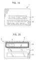
- Fig. 19 is a plan showing an example structure of an embossed card 1 according to a conventional method.
- the embossed card shown in Fig. 19 has embossable areas A1 and A2 assigned at locations on a card member which are specified in advance by a JIS standard.
- embossed symbols such as "0123 456 789" are formed as the membership number and the expiration date of the card owner.
- embossed letters indicating the party who issues the card, such as "ABC Corporation IC Card," and the name of the card owner are formed.
- the letter and symbol information of the card owner formed in the embossable areas A1 and A2 is read by an information transfer means for use solely with an embossment information and the membership number and the expiration date of the card owner are transferred to a predetermined sheet in a so-called card payment systems. With these operations, a proof of the transaction remains, and the transaction amount is charged directly to the account of the card owner later.
- card payment systems are currently used in various banks, golf courses, credit card companies, and others.
- the card Since such an IC card is of a non-contact type electrically, information is read from or written into the card by a special card reader and writer. To this end, the card has an antenna body and an IC chip in it.
- the card reader and writer supplies electrical power to the card in the form of electromagnetic energy and a DC voltage is generated within the card when information is read from or written into the card because, if the card is provided with a power supply, the maintenance thereof is troublesome and increases cost, and the power supply is an obstacle to making the card thinner.
- the IC card In such a card reading system, electromagnetic waves in the short-wave frequency band (13.56 MHz) are used. Because the card size is much smaller than the wavelength of the electromagnetic waves, it is very inefficient and difficult to receive electric-field energy in the IC card having a dipole antenna in it. Therefore, the IC card is provided with a loop antenna to receive electromagnetic energy by electromagnetic coupling. In this case, a card loop-antenna body having a good receiving efficiency is required.
- embossable IC cards are demanded from which letter and symbol information of the card owner is read by both existing information transfer apparatuses for use solely with embossment information and card readers and writers for new systems.
- a loop antenna mounted within the IC card may be broken.
- a method is considered for providing a loop antenna body 5 formed by arranging a thin antenna pattern 5A in a loop manner so as to avoid the embossable areas A1 and A2 disposed at the locations specified by the JIS standard in an embossed card 2 having an electronic component in it, as shown in Fig. 20.
- the receiving efficiency decreases since the area where the loop antenna body 5 is coupled with an electromagnetic field is considerably smaller than the card size, the receiving efficiency decreases.
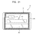
- a method for extending a loop antenna body 6 so as to have almost the same size as the card in an embossed card 3 having an electronic component in it, as shown in Fig. 21.
- This method extends the coupling area with an electromagnetic field, but a thin antenna pattern 6A may be broken if a letter or a symbol is embossed at a portion outside the embossable area A2 since the thin antenna pattern 6A is disposed close to the embossable area A2.
- the function of the loop antenna body 6 is impaired and the reliability of the embossable IC card 3 is impaired.
- the present invention has been made in consideration of the above conditions. Accordingly, it is an object of the present invention to provide an embossable IC card in which an antenna pattern is prevented from being broken even if a letter or a symbol is formed at the antenna pattern outside an embossable area on the card member, and which allows a system which uses the card to operate smoothly; a manufacturing method of the card; and an information reading and confirming system for the card.
- an embossable IC card including a first card member having an embossable area where embossing is to be performed; a second card member disposed opposite the first card member; an IC chip sandwiched by the first and second card members; and an antenna pattern disposed around the IC chip and connected to the IC chip, wherein the width of the antenna pattern is wider than the longitudinal length of the largest letter or symbol to be embossed in the embossable area.
- an embossable IC card of the present invention since the width of the antenna pattern is made wider than the longitudinal length of the largest embossed letter or symbol formed in the embossable area by embossing, even if a letter or a symbol is formed at the antenna pattern outside the embossable area, a part of the antenna pattern is always left. Therefore, even if a letter or a symbol is formed outside the embossable area, the antenna pattern is prevented from being broken.
- a transaction amount is automatically charged at the site according to the letter and symbol information of the card owner read from the IC chip of the IC card.
- embossment information letter and symbol information (hereinafter called embossment information) printed in a stand-out manner on the card is transferred to a slip by using an information transfer apparatus for use solely with embossment information, and the slip is left as proof of the transaction. Therefore, the transaction amount is automatically charged to the bank account of the customer later.
- an IC card including a first card member having an embossed area where embossing has been performed; a second card member disposed opposite the first card member; an IC chip sandwiched by the first and second card members; and an antenna pattern disposed around the IC chip and connected to the IC chip, wherein the width of the antenna pattern is wider than the longitudinal length of the largest embossed letter or symbol formed in the embossed area.
- the foregoing object is achieved in still another aspect of the present invention through the provision of a transaction confirming method by using an IC card, the IC card including a first card member having embossed data formed in an embossed area; a second card member disposed opposite the first card member; an IC chip sandwiched by the first and second card members; and an antenna pattern disposed around the IC chip and connected to the IC chip, wherein the width of the antenna pattern is wider than the longitudinal length of the largest embossed letter or symbol formed in the embossed area, and the transaction confirming method including the steps of: reading the embossed data formed in the IC card; and reading information recorded in the IC chip from the IC card and performing transaction processing.
- the present invention has been made in consideration of a condition in which, when usual embossed cards are exchanged for electronic cards, it is thought that information transfer means for use solely with embossment information being simultaneously changed to data processing means for IC cards during the transition will be very rare, but, rather, the transition to new systems will happen gradually.
- a transaction confirming method by using an IC card of the present invention, at a site where data processing means dedicated to IC cards is installed, the letter and symbol information of the card owner, read from the IC chip is read, and transactional processing is achieved.
- the letter and symbol information of the card owner printed in a stand-out manner in an embossable area is transferred to a slip by using information transfer means dedicated to embossment information, and the slip is left as the proof of the transaction. Therefore, the transactional bill is automatically charged to the bank account of the customer later.
- the width of a portion of an antenna pattern, which is disposed along an embossable area is made wider than the longitudinal length of the largest letter formed by embossing.
- a transaction confirming method by using an IC card according to the present invention is provided with information transfer means for use solely with embossment information, for transferring the information related to the card owner formed in an embossable area to a sheet, or data processing means for IC cards for reading the information related to the card owner recorded in an IC chip and for achieving predetermined transaction processing.
- the information related to the card owner read from the IC chip is read and transaction processing is achieved, and at a site where the data processing means is not installed, the information related to the card owner printed in a stand-out manner in an embossable area is transferred to a slip by the information transfer means and the slip is left as proof of the transaction.
- the present invention is suited to a non-contact-type IC cards used as bank cards, cash cards, and credit cards on which letters can be embossed, and operation systems for the IC cards.
- Fig. 1 is a perspective view showing an example structure of an embossable IC card 100 according to an embodiment of the present invention.
- Fig. 2 is a mounting image view showing an example structure of an embossable card 101 having a built-in electronic component according to a first embodiment.
- Fig. 3 is a plan showing an example structure of an electronic component 11.
- Fig. 4 is a view showing possible relationships between thick antenna patterns 12B and letter and symbol dimensions.
- Fig. 5 is a view showing an example of formed letter and symbol information.
- Fig. 6 is an outlined view showing an example structure of an embossable card 102 having a built-in electronic component according to a second embodiment.
- Fig. 7 is a plan showing an example structure of an electronic component 21.
- Fig. 8 is an outlined view showing an example structure of an embossable card 103 having a built-in electronic component according to a third embodiment.
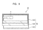
- Fig. 9 is a plan showing an example structure of an electronic component 31.
- Fig. 10 is a perspective view of an example manufacturing process (No. 1) for embossable IC cards, according to an embodiment.
- Fig. 11A and Fig. 11B are a cross-sectional view and a plan view showing an example of a manufacturing process (No. 2) for embossable IC cards, according to the embodiment.
- Fig. 12A, Fig. 12B, and Fig. 12C are a cross-sectional view taken on the line XIIA-XIIA, a plan view, and a cross-sectional view taken on the line XIIC-XIIC showing an example of a manufacturing process (No. 3) for embossable IC cards, according to the embodiment.
- Fig. 13A, Fig. 13B, and Fig. 13C are a cross-sectional view taken on the line XIIIA-XIIIA, a plan view, and a cross-sectional view taken on the line XIIIC-XIIIC showing an example of a manufacturing process (No.4) for embossable IC cards, according to the embodiment.
- Fig. 14A, Fig. 14B, and Fig. 14C are a cross-sectional view taken on the line XIVA-XIVA, a plan view, and a cross-sectional view taken on the line XIVC-XIVC showing an example of a manufacturing process (No. 5) for embossable IC cards, according to the embodiment.
- Fig. 15 is a perspective view showing an example of a structure of an information reading and confirming system 200 for embossed IC cards, according to an embodiment.
- Fig. 16 is a block diagram showing an example of an internal structure of the electronic component 11 of the embossed card 100 having the built-in electronic component according to the embodiment.
- Fig. 17 is a block diagram showing an example of an internal structure of a card reader/writer 33, according to an embodiment.
- Fig. 18 is a flowchart showing an example processing of the information reading and confirming system for embossed cards having a built-in electronic component, according to an embodiment.
- Fig. 19 is a plan showing an example structure of an embossed card 1 according to a conventional method.
- Fig. 20 is a view showing an example structure of an embossed card 2 having a built-in electronic component, according to the conventional method.
- Fig. 21 is a view showing an example structure of an embossed card 3 having a built-in electronic component, according to the conventional method.
- Fig. 1 is a perspective view showing an example structure of an embossable IC card 100 according to an embodiment.
- the width of an antenna pattern disposed along an embossable area of a card member is made wider than the longitudinal length of the largest embossed letter or symbol formed by embossing. Therefore, even if a letter or a symbol is formed at the antenna pattern outside the embossable area, the antenna pattern is prevented from being broken. In addition, the operation of a system using the card is made smooth.
- the embossable IC card 100 is a non-contact electronic card, and has a laminate structure in which an electronic component is sandwiched by front and rear card members 7 and 8 both having a length of L mm and a width of W mm, as shown in Fig. 1.
- embossable areas A1 and A2 are formed at locations specified in advance.
- the two embossable areas A1 and A2 are assigned to one card 100; in the embossable area A1 disposed almost at the center of the card, embossed symbols such as those for the membership number and the expiration date of the card owner are formed.
- embossed letters such as those for the party who issues the card and the name of the card owner are formed.
- embossed letters and embossed symbols are also called hereinafter embossment information.
- the embossed letters and symbols are formed by an embossing apparatus not shown.
- the IC card 100 is sandwiched by metal dies and pressed to form relatively shallow embossed letters and symbols. Unlike coining, since the protrusions and recesses of the dies face each other, the thickness of the card, including an area where letters and symbols are embossed, is little changed.
- the electronic component 11 sandwiched by the front and rear card members 7 and 8 is formed of an IC chip 4, and a loop antenna body 12 disposed around the IC chip 4, for example, disposed so as to surround the IC chip 4, and connected to the IC chip 4.
- the loop antenna body 12 thin antenna patterns 12A and thick antenna patterns 12B are connected in series and in a loop manner, and form, for example, a three-turn antenna pattern.
- Fig. 2 is a mount image view showing an example structure of an embossable card 101 having a built-in electronic component according to a first embodiment.
- the embossed letter or symbol having the maximum longitudinal length is extracted in advance among embossed letters and symbols which can be used in the first and second embossable areas A1 and A2, and the width B of thick antenna patterns 12B passing under the embossable areas A1 and A2 is made wider than the longitudinal length A of the largest embossed letter or symbol.
- the embossable card 101 having a built-in electronic component shown in Fig. 2 has a length of about 90 mm and a width W of 60 mm, and has a laminate structure in which an electronic component 11 is sandwiched by the front and rear card members 7 and 8.
- the electronic component 11 has an IC chip 4 and a loop antenna body 12.
- Fig. 2 to make the card structure easy to understand, only the embossable areas A1 and A2 are shown in the front card member 7.
- one line of a thick antenna pattern 12B is disposed under the first embossable area Al, and two lines of thick antenna patterns 12B are disposed under the second embossable area A2.
- the width B of the thick antenna patterns 12B passing under the embossable areas A1 and A2 is made wider than the longitudinal length A of the largest embossed letter or symbol formed by the embossing apparatus.
- the width B of the thick antenna patterns 12B is set to about 8 mm. The difference ⁇ therebetween is assured by about 1 mm.
- thin antenna patterns 12A about 1 mm wide and thick antenna patterns 12B about 8 mm wide (B) are connected in series and in a loop manner to form, for example, a three-turn antenna pattern. Both ends of the antenna pattern are connected to the IC chip 4 and a capacitor not shown, and these electronic parts have a remote IC function.
- the capacitor is used to make receiving efficiency as high as possible by tuning the loop antenna body 12 into the carrier frequency of an electromagnetic field. When it is allowed that receiving efficiency is lowered, the capacitor may, of course, be omitted.
- the carrier frequency is about 13.56 MHz.
- the IC card 101 Since the IC card 101 is of a non-contact type, it is not provided with a terminal for information input and output.
- This embossable card 101 receives an electromagnetic field in which information has been converted to a predetermined modulated electric wave by the L times W loop antenna body 12 having almost the same size as the IC card. Therefore, almost the same receiving efficiency as that of a thin antenna pattern formed in a loop manner by the conventional method is obtained.
- the predetermined modulated electric wave received by the loop antenna body 12 is demodulated by the IC chip 4 and written into a non-volatile memory, and the information is read from the memory.
- the driving power source of the IC chip is obtained from external electromagnetic energy by the loop antenna body 12.
- the electromagnetic field received by the loop antenna body 12 is converted to induced electromotive force according to the law of electromagnetic induction, the electromotive force is rectified to obtain a DC power source, and the DC voltage is sent to the IC chip 4.
- a power source of 2.2 V at about 1 mA is obtained. Electricity may, of course, be obtained from an external high-frequency electromagnetic energy by the loop antenna body 12 or other elements in addition to this DC power.
- Fig. 4B shows a case in which embossed letters and symbols "ooo” of "ooo ⁇ ⁇ ⁇ " are formed beyond the upper edge of the thick antenna pattern 12B.
- a portion having a width of 1 mm or more of the antenna pattern is left at the lower edge. Therefore, even when embossed letters and symbols are made around the upper side of the thick antenna pattern 12B by an embossing apparatus to go through the antenna pattern, the antenna pattern is still connected at some location and the loop antenna body 12 is prevented from being broken.
- Fig. 4C shows a case in which the embossed letters and symbols "ooo ⁇ ⁇ ⁇ " are formed beyond the lower edge of the thick antenna pattern 12B.
- a portion having a width of 1 mm or more of the antenna pattern is left at the upper edge. Therefore, even when embossed letters and symbols are made around the lower side of the thick antenna pattern 12B by an embossing apparatus to go through the antenna pattern, the antenna pattern is still connected at some location and the loop antenna body 12 is prevented from being broken.
- Fig. 5 shows an example of embossed letters and symbols formed in the embossable areas A1 and A2.
- embossed symbols such as "0123 456 789” are formed as the membership number and the expiration date of the card owner.
- embossed letters are formed such as the party who issues the card, "ooo Corporation Felica IC Card," and the name of the card owner.
- the embossable card 101 having an electronic component in it, of the first embodiment although the thick antenna patterns 12B are formed below the embossable areas A1 and A2, and since the loop antenna body 12 has almost the same size as the IC card, the loop antenna body 12 has the same receiving efficiency as that formed of a usual thin antenna pattern.
- embossed letters and symbols can be formed at any locations in the embossable areas A1 and A2. Therefore, the reliable, embossable IC card 101 is provided.
- FIG. 6 is an outlined view showing an example structure of an embossable card 102 having an electronic component in it, according to a second embodiment.
- a card member 7 is provided with two embossable areas A1 and A2, and an antenna pattern 22C is formed between the embossable areas A1 and A2.
- the number of antenna patterns passing therebetween is not limited to one.
- the embossable card 102 having an electronic component in it, shown in Fig. 6, has the same size as in the first embodiment, and has a laminate structure in which front and rear card members 7 and 8 sandwich an electronic component 21.
- the electronic component 21 is formed of an IC chip 4 and a loop antenna body 22. Also in Fig. 6, to make the card structure easy to understand, only the embossable areas A1 and A2 are shown in the front card member 7.
- one line of a thick antenna pattern 22B is disposed below each of the first and second embossable areas A1 and A2, and the antenna pattern 22C having a predetermined width is disposed between the two embossable areas A1 and A2.
- the thin antenna pattern 12A described in the first embodiment may be of course used as the antenna pattern disposed between the embossable areas A1 and A2. It is preferred that an antenna pattern having a width wider than the distance between the embossable areas be used. This is because, even when embossed letters and symbols are made by an embossing apparatus to go through the antenna pattern 22C, the antenna pattern is still connected at some location and the loop antenna body 22 is prevented from being broken.
- thin antenna patterns 22A about 1 mm wide, the antenna pattern 22C about 2 mm wide, and the thick antenna pattern 22B about 8 mm (B) wide are connected in series and in a loop manner to form, for example, a three-turn antenna pattern. Both ends of the antenna pattern are connected to the IC chip 4 and a capacitor not shown. These electronic elements have a remote IC function. In this embodiment, a power is supplied in the same way as in the first embodiment.
- This loop antenna has almost the same receiving efficiency as that formed of a thin antenna pattern made in a loop manner by the conventional method.
- three antenna patterns may be formed in the two embossable areas A1 and A2. Embossment information can be made without any restrictions. In this case, when the antenna patterns disposed at both sides which sandwich the center one is made wide, the loop antenna body 22 is prevented from being broken even if a positional shift occurs in mounting The antenna patterns disposed at both sides may be located below the embossable areas A1 and A2.
- the antenna pattern 22C having a predetermined width is disposed between the two embossable areas Al and A2, the area where the loop antenna is coupled with the electromagnetic field is reduced.
- the thick antenna pattern 22B is disposed below the embossable area A2 to make the loop antenna body 22 having almost the same size as the IC card. Letters and symbols can be embossed in these embossable areas without reducing the receiving efficiency from that of a three-turn loop antenna body formed of a usual thin antenna pattern. Therefore, the highly reliable, embossable IC card 102 is provided.
- Fig. 8 is an outlined view showing an example structure of an embossable card 103 having a built-in electronic-component according to a third embodiment.
- a card member 7 is provided with embossable areas A1 and A2, and an antenna pattern 32C having a predetermined width is disposed along the card edge under the embossable area A2.
- the number of the antenna pattern 32C passing under the area is not limited to one.
- the embossable card 103 having a built-in electronic component shown in Fig. 8 has the same size as in the first and second embodiments, and has a laminate structure in which front and rear card members 7 and 8 sandwich an electronic component 31.
- the electronic component 31 has an IC chip 4 and a loop antenna body 32. Also in Fig. 8, to make the card structure easy to understand, only the embossable areas A1 and A2 are shown in the front card member 7.
- one line of a thick antenna pattern 32B is disposed below each of the first and second embossable areas A1 and A2, and the antenna pattern 32C having a predetermined width is disposed along the card edge under the embossable area A2.
- the thin antenna pattern described in the first embodiment may be of course used as the antenna pattern 32C disposed below the embossable area A2. It is preferred that an antenna pattern having a width wider than the thin antenna pattern be used. This is because, even when embossed letters and symbols are made by an embossing apparatus to go through the antenna pattern 32C, the antenna pattern is still connected at some location and the loop antenna body 32 is prevented from being broken.
- thin antenna patterns 32A about 1 mm wide
- the antenna pattern 32C about 3 mm wide
- the thick antenna patterns 32B about 8 mm (B) wide are connected in series and in a loop manner to form, for example, a three-turn antenna pattern. Both ends of the antenna pattern are connected to the IC chip 4 and a capacitor not shown. These electronic elements have a remote IC function.
- a power is supplied in the same way as in the first embodiment.
- This loop antenna has almost the same receiving efficiency as that formed of a thin antenna pattern made in a loop manner in the conventional method.
- Three antenna patterns may be formed below the embossable area A2. Embossment information can be made without any restrictions. In this case, when the antenna patterns disposed close to the embossable area A2 is made wide, the loop antenna body 32 is prevented from being broken even if a positional shift occurs in mounting.
- the antenna patterns disposed close to the embossable area A2 may be located below the embossable area A2.
- the antenna pattern 32C having a predetermined width is disposed along the card edge below the embossable area A2, and the loop antenna body 32 having almost the same size as the IC card is formed.
- Letters and symbols can be embossed in these embossable areas A1 and A2 without reducing the receiving efficiency from that of a three-turn loop antenna body formed of a usual thin antenna pattern. Therefore, the highly reliable, embossable IC card 103 is provided.
- Fig. 10 to Fig. 14C are views showing examples of manufacturing processes (No. 1 to No. 5) of embossable IC cards according to an embodiment.
- a card member having embossable areas at predetermined locations thereof is formed; antenna patterns are formed in a loop manner of which portions disposed along the embossable areas have widths wider than the longitudinal length of the largest embossed letter or symbol made by embossing; then, the antenna patterns are connected to an IC chip to form an electronic component; and the electronic component is sandwiched by the card members.
- the IC cards 101 described in the first embodiment are formed in a connected manner on a long sheet, and then, each IC card 101 is punched out from the sheet.
- a front card member 7 having embossable areas A1 and A2 at predetermined locations thereof and a rear card member 8 are formed. These card members 7 and 8 are printed on long-sheet film resin and wound like a role.
- the first and second embossable areas A1 and A2 are specified in printing according to a JIS standard.
- a long-sheet substrate 13 having copper-foil patterns 14A and 14B on both side thereof is prepared, as shown in Fig. 11A.
- the shape of the substrate 13 is of course not limited to a long-sheet shape, but may be a card shape.
- the front and rear copper foil patterns 14A and 14B have a thickness of about several dozen to several hundred micrometers, and are used to form a thick antenna pattern, a thin antenna pattern, an antenna pattern having a predetermined width, and an electrode of a capacitor.
- Fig. 11A is a cross-sectional view of the substrate 13 having the copper foil patterns on both sides thereof, and Fig. 11B is a plan thereof.
- the loop antenna body 1 described in the first embodiment it is better to form in advance through holes 15A and 15B at predetermined positions, as shown in Fig. 11B. These through holes 15A and 15B electrically connect the front and rear copper foil patterns.
- a reticle having an image of the loop antenna body 12 is made. in the reticle, the width of the portions corresponding to antenna patterns disposed along the embossable areas on the front card member 7 is made wider than the longitudinal length of the largest embossed letter or symbol formed by an embossing apparatus.
- the portion corresponding to a thin antenna pattern 12A is about 0.7 to 1.0 mm wide
- the portion corresponding to a thick antenna pattern 12B is about 7 mm to 10 mm wide.
- a resist film not shown is applied to the surface of one of the copper foil patterns with the positions of the through holes 15A and 15B shown in Fig. 11B being used as references.
- the resist film is exposed to light with the reticle being used as a mask.
- the copper foil pattern is removed from the substrate by the use of a predetermined etching solution.
- the substrate is then washed with water to form the loop antenna body 12 formed of a sheet-shaped coil patterns, and an accumulation electrode not shown, on the substrate, as shown in Fig. 12B.
- Etching is also applied to the copper foil pattern 14B formed on the rear side of the substrate to leave a portion 141 serving as the bottom of an IC-chip mounting zone and an antenna pattern 142 for connection which crosses antenna patterns (as shown in Fig. 12A and Fig. 12C).
- the antenna pattern 142 for connection is electrically connected to antenna patterns 121 and 12B formed on the front surface by the through holes 15A and 15B (indicated by black circles in the figure). Then, the front surface of the substrate shown in Fig. 12A is selectively removed to make an opening. It is preferred that an IC-chip-mounting opening section 16 be formed which uses the copper foil pattern 141 formed on the rear surface of the substrate as the bottom.
- FIG. 12A is a cross-sectional view taken on the line XIIA-XIIA of Fig. 12B
- Fig. 12C is a cross-sectional view taken on the line XIIC-XIIC of Fig. 12B.
- Fig. 13A is a cross-sectional view taken on the line XIIIA-XIIIA of Fig. 13B
- Fig. 13C is a cross-sectional view taken on the line XIIIC-XIIIC of Fig. 13B.
- the electronic component 11 is sandwiched by the card members 7 and 8, and sealed.
- epoxy-resin adhesive members are applied to the opposing surfaces of the long-sheet card members 7 and 8.
- the long-sheet electronic component 11 is sandwiched by the card members 7 and 8 and they are pasted with each other at a predetermined temperature and pressure as shown in Fig. 14A.
- the long-sheet IC cards 101 are formed, as shown in Fig. 14C. After the sheet-shaped IC cards 101 is hardened, each IC card 101 is punched. An embossable card having a built-in electronic component is thus manufactured.
- Fig. 14A epoxy-resin adhesive members
- Fig. 14A is a cross-sectional view taken on the line XIVA-XIVA of Fig. 14B
- Fig. 14C is a cross-sectional view taken on the line XIVC-XIVC of Fig. 14B.
- embossable cards having a built-in electronic component are manufactured at a high reproducibility. Even when an embossed letter or symbol is formed at the loop antenna body 1? outside the embossable areas of the card members 7 and 8 to go through the loop antenna body, since a part of the thick antenna patterns 12B always remains, if a letter or a symbol is formed outside the embossable areas, the loop antenna body is prevented from being broken.
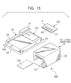
- Fig. 15 is a perspective view showing an example structure of an information reading and confirming system 200 for embossed IC cards, according to an embodiment of the present invention.
- an embossed IC card 100 having an IC chip and an antenna pattern is prepared in advance.
- the information related to the card owner recorded in the IC chip is read and predetermined transaction processing is achieved.
- the information related to the card owner formed in an embossable area is read by information transfer means for use solely with embossment information to transfer it to a sheet. The amount of the transaction is automatically charged later.
- the information reading and confirming system 200 for embossed IC cards shown in Fig. 15 is very suited not only to cash payment systems but also to credit-card payment systems in various transactions.
- the above-described embossed IC cards 100 are used in the system 200.
- Each of these IC cards 100 has the embossable areas A1 and A2 at positions specified in advance of the card member 7 and has the IC chip 4 and the loop antenna body 12 sandwiched by the front and rear card members 7 and 8 (as shown in Fig. 1).
- This system 200 is at least provided with information transfer means 24 for use solely with embossment information.
- the information transfer means 24 is provided with a table (base) 25 for placing a card and papers.
- the IC card 100 is placed on the table 25 and secured.
- a stepped section 25A for placing papers is provided at one end of the table 25, a stepped section 25A for placing papers is provided. Papers 40 are placed such that one side thereof is butted against the stepped section 25A.
- the papers 40 are formed of a plurality of sheets having a predetermined duplicating function.
- the papers 40 have a predetermined recording area.
- the information related to the card owner is transferred from the embossed card and recorded.
- a slider 26 is provided at a side of the table 25.
- a handle 27 which is movable to the right and to the left is mounted to the slider 26. The handle 27 is operated, for example, so as to reciprocate to the right and left along the slider 26 while being pressed downwards.
- the card 100 is placed on the table 25 with the surface on which embossed letters and symbols are formed facing upwards, then the papers 40 having a duplicating function are placed on the card 100 along the stepped section 25A. Under this condition, the handle 27 is operated so as to reciprocate to the right and left along the slider 26 while being pressed downwards. With these operations, the information related to the card owner is duplicated from the embossed card 100 to the predetermined recording area of the papers 40 and recorded.
- the system 200 is provided with a card reader/writer 33 serving as data processing means for IC cards.
- the card reader/writer 33 has a card insertion slot 34, where the card 100 is inserted.
- the card reader/writer 33 reads the information related to the card owner recorded in the IC chip 4 of the card 100.
- the information related to the card owner formed in an embossable area is recorded into the IC chip 4 of the IC card to prevent card forgery.
- an upper business computer not shown is provided in addition to the card reader/writer 33 to achieve predetermined transaction processing according to the information related to the card owner.
- the information related to the card owner is read from the IC chip 4 of the card 100 or predetermined information related to a transaction is written into the IC chip 4.
- the information related to the card owner printed in a stand-out manner at embossable areas A1 and A2 are transferred to a slip by using the information transfer means 24, and the slip is left as proof of the transaction.
- a control apparatus is provided for the card reader/writer 33 or for the upper computer to compare and verify the information related to the card owner formed in the embossable areas A1 and A2 and that recorded in the IC chip 4 of the IC card.
- the information related to the card owner formed in the embossable area is read by a letter recognition apparatus such as an OCR. If the letter and symbol information formed on the front surface of the card differs from that recorded in the card, alarm processing is achieved and the card is forcedly discharged.
- Fig. 16 is a block diagram showing an example of an internal structure of the electronic component 11.
- the electronic component 11 shown in Fig. 16 has the IC chip 4 and the loop antenna body (receiving means) 12.
- the IC chip 4 includes a modulation and demodulation circuit 41 and a signal processing circuit 42.
- the signal processing circuit 42 has a non-volatile memory not shown.
- the loop antenna body 12 is connected to the modulation and demodulation circuit 41.
- a modulated wave (13.56 MHz) received by the loop antenna body 12 is demodulated by the demodulation function of the modulation and demodulation circuit 41.
- a data sequence (Data: R to C) sent from the card reader/writer 33 to the card 100 is demodulated.
- the demodulated data sequence is sent from the modulation and demodulation circuit 41 to the signal processing circuit 42.
- the signal processing circuit 42 applies decoding processing to the demodulated data sequence, and information is read from the non-volatile memory according to the result of the decoding, or recording data included in the data sequence is written into the memory.
- the information read from the non-volatile memory is, for example, ASK-modulated by the modulation function of the modulation and demodulation circuit 41 to form a data sequence (Data: C to R) and the data sequence is sent to the card reader/writer 33 through the loop antenna body 12.
- Data A part of the electromagnetic field emitted from the card reader/writer 33 is converted to an electrical signal and used as a power source of the card 100.
- the modulation and demodulation circuit 41 has a power-source generating function, and converts electromagnetic energy to a stable DC electrical power. All circuits in the IC card 100 are operated by this power source.
- FIG. 17 is a block diagram showing an example of an internal structure of the card reader/writer 33 according to an embodiment of the present invention.
- the card reader/writer 33 shown in Fig. 17 is also provided with a loop antenna body 52 to allow communications with the IC card 100.
- the loop antenna body 12 of the card 100 and the loop antenna body 52 of the card reader/writer 33 are electromagnetically coupled and used in an electrically non-contact state.
- the loop antenna body 52 is connected to a modulation and demodulation circuit 51, and a modulated wave sent from the card 100 is demodulated by the demodulation function of the circuit 51.
- a data sequence (Data: C to R), including the membership number of the card owner and the expiration date of the card, sent from the card 100 to the card reader/writer 33 is demodulated.
- the data sequence is configured according to a predetermined data format.
- One packet of the data sequence is, for example, formed of a header and data.
- the modulation and demodulation circuit 51 is connected to a signal processor unit (hereinafter called an SPU) 53.
- the SPU 53 includes a central processing unit (CPU) not shown for achieving various types of calculation processing, a ROM storing a control program, and a general-purpose RAM used as a work memory.
- the SPU 53 applies various types of data processing to the demodulated information according to the control program read from the ROM, and outputs, for example, information to be written into the IC card 100 to the modulation and demodulation circuit 51.
- the modulation and demodulation circuit 51 modulates various types of information received from the SPU 53, and then, sends a data sequence (Data: R to C) to the IC card 100 through the loop antenna body 52 in the form of a modulated radio wave.
- Data data: R to C
- the data sequence is ASK-modulated by the use of a carrier wave having a frequency of 13.56 MHz and the modulated radio wave is sent to the IC card 100 as an electromagnetic field (about 500 ( ⁇ V/m) by the loop antenna body 52.
- a power supply and control section 57 is connected to the modulation and demodulation circuit 51, the SPU 53, an input tool 54, and a display 55 to send DC power.
- the power supply and control section 57 sends a carrier wave having a frequency of 13.56 MHz to the modulation and demodulation circuit 51.
- the input tool 54 such as a keyboard, is connected to the SPU 53.
- the operator manipulates the input tool 54 to give an instruction to the SPU 53.
- the display 55 is also connected to the SPU 53. Information read from the card 100 and information to be written into the card 100 are displayed on the display 55 for confirmation.
- the SPU 53 is also connected to an external apparatus 56, such as an upper computer, to allow a transaction to be automatically billed on-line.
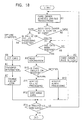
- Fig. 18 is a flowchart of the example processing to be achieved by the information reading and confirming system 200 for embossed cards having a built-in electronic component, according to an embodiment of the present invention.
- an embossed IC card 100 having an IC chip and an antenna pattern is prepared in advance; and when various transactions are made and the amounts of the transactions are charged by the card, at a site where data processing means for the IC card is installed, the information related to the card owner recorded in the IC chip is read and predetermined transaction processing is achieved, and at a site where data processing means of this type is not installed, the information related to the card owner formed in an embossable area is read by information transfer means for use solely with embossment information to transfer it to a sheet and the amounts of the transactions are automatically charged later.
- the card 100 of this type can be used in current restaurants, various installment sales shops, gas stations, and banks, and actually used at least when the information transfer means 24 for use solely with embossment information is provided and a bank account of the card owner has been opened. It is required that data processing means for IC cards be connected on-line to banks.
- step A2 the card owner determines whether the owner pays the amounts of the transactions in cash or by card.
- the processing proceeds to step A3, and the amounts of the transactions are paid in cash.
- the processing proceeds to step A4.
- step A4 whether the data processing means for IC cards is used on-line or the information transfer means 24 for use solely with embossment information is used off-line is determined.
- the processing proceeds to step A5, and the card 100 is placed in the information transfer means 24.
- the card 100 is actually placed on the table 25 with the surface on which embossed letters and symbols have been formed being placed upwards.
- the papers 40 having a duplicating function, such as slips, related to the transactions are placed along the stepped section 25A.
- the handle 27 of the information transfer means 24 is operated to reciprocate to the right and left along the slider 26 while being pressed downwards in step A6.
- the information related to the card owner is duplicated from the embossed card 100 to the predetermined recording area of the papers 40 and recorded.
- the information related to the card owner printed in a stand-out manner in the embossable areas A1 and A2 have been transferred to the slips, and they remain as a proof of the transactions.
- step A7 the amounts of the transactions are charged at the bank account of the card owner according to the papers 40.
- step A4 when the card reader/writer 33 has been installed, the processing proceeds to step A8, and the card reader/writer 33 waits for a card to be inserted. The card owner inserts the card 100 into the card insertion slot 34 of the card reader/writer 33.
- step A9 the card reader/writer 33 reads letter and symbol information, such as the membership number and the expiration date of the card owner, from the IC chip 4. Then, the processing proceeds to step A10, where it is determined whether the card is genuine or an imitation. This determination is achieved by comparing the information related to the card owner formed in the embossable areas A1 and A2 with that recorded in the IC chip 4 of the IC card. When it is determined from the result of comparison that the card is genuine in step A10, the processing proceeds to step A11, and on-line processing is performed such as the automatic charge of the amounts of the transactions at the bank account of the card owner. Predetermined information related to the transactions may be written. Then, the processing proceeds to step A12, and the card 100 is discharged normally. When it is determined in step A10 that the card is an imitation, the processing proceeds to step A13, alarm processing is conducted, and the card 100 is forcedly discharged.
- step A10 the card reader/writer 33 reads letter and symbol information, such as the membership number and the expiration
- step A14 it is determined whether the processing of the information reading and confirming system is terminated.
- a system available time is specified in advance, the operation is terminated when the available time elapses.
- the processing returns to step A1 and the processing is repeated from step A1 to step A14 until an event which needs a halt occurs.
- the information reading and confirming system 200 for embossed IC cards of the present invention at a site where data processing means for use solely with the IC cards is installed, the information related to the card owner read from the IC chip 4 is read and transaction processing is achieved, and at a site where the data processing means is not installed, the information related to the card owner printed in a stand-out manner in an embossable area is transferred to a slip by the information transfer means 24 for use solely with embossment information and the slip is left as proof of the transaction.
- the amount of the transaction is automatically charged at the bank account of the customer later.
- the embossed IC card 100 and the information reading and confirming system 200 work sufficiently well.
- one apparatus reads the embossed area and another apparatus reads information recorded in the IC chip mounted in the IC card.
- a transaction confirming and information reading method by using an IC card when a card transaction terminal apparatus is used, such as an automatic teller machine (ATM) having an optical sensor for reading embossed data and a reader/writer for transmitting and receiving data in the IC chip through an antenna, a multimedia terminal, or a cash dispenser, transaction is confirmed and information is read by the use of only one apparatus.
- the card transaction terminal apparatus such as an ATM may include magnetic-data reading means for reading magnetic data formed in the IC card, in addition to the above-described reading section.
Applications Claiming Priority (2)
| Application Number | Priority Date | Filing Date | Title |
|---|---|---|---|
| JP35209299 | 1999-12-10 | ||
| JP35209299A JP2001167242A (ja) | 1999-12-10 | 1999-12-10 | エンボス加工可能なicカード、その製造方法及びその情報読取確認システム |
Publications (2)
| Publication Number | Publication Date |
|---|---|
| EP1107175A2 true EP1107175A2 (fr) | 2001-06-13 |
| EP1107175A3 EP1107175A3 (fr) | 2002-05-22 |
Family
ID=18421737
Family Applications (1)
| Application Number | Title | Priority Date | Filing Date |
|---|---|---|---|
| EP00403455A Withdrawn EP1107175A3 (fr) | 1999-12-10 | 2000-12-08 | Carte à puce embossée et lecteur de cette carte |
Country Status (5)
| Country | Link |
|---|---|
| US (1) | US20010030238A1 (fr) |
| EP (1) | EP1107175A3 (fr) |
| JP (1) | JP2001167242A (fr) |
| CN (1) | CN1300036A (fr) |
| SG (1) | SG85224A1 (fr) |
Cited By (7)
| Publication number | Priority date | Publication date | Assignee | Title |
|---|---|---|---|---|
| FR2893164A1 (fr) * | 2006-08-31 | 2007-05-11 | Oberthur Card Syst Sa | Procede de fabrication d'une carte a micro-circuit, notamment a antenne magnetique. |
| WO2007054632A1 (fr) * | 2005-11-08 | 2007-05-18 | Oberthur Technologies | Procede de fabrication d'une carte a microcircuit et carte a microcircuit, notamment a antenne magnetique |
| US8111136B2 (en) | 2009-01-23 | 2012-02-07 | Shining Union Limited | USB fingerprint scanner with touch sensor |
| US8111135B2 (en) | 2009-01-23 | 2012-02-07 | Shining Union Limited | USB fingerprint scanner with touch sensor |
| US8279044B2 (en) | 2008-10-10 | 2012-10-02 | Shining Union Limited | Data storage device with radio frequency fingerprint scanner |
| EP2710523B1 (fr) | 2011-05-17 | 2016-08-17 | Gemalto SA | Dispositif transpondeur radiofrequence a circuit resonant passif optimise |
| FR3033435A1 (fr) * | 2015-03-04 | 2016-09-09 | Smart Packaging Solutions | Carte a puce sans contact avec antenne optimisee pour permette l'embossage des caracteres |
Families Citing this family (33)
| Publication number | Priority date | Publication date | Assignee | Title |
|---|---|---|---|---|
| US7156301B1 (en) * | 1999-09-07 | 2007-01-02 | American Express Travel Related Services Company, Inc. | Foldable non-traditionally-sized RF transaction card system and method |
| US7239226B2 (en) | 2001-07-10 | 2007-07-03 | American Express Travel Related Services Company, Inc. | System and method for payment using radio frequency identification in contact and contactless transactions |
| US7837116B2 (en) | 1999-09-07 | 2010-11-23 | American Express Travel Related Services Company, Inc. | Transaction card |
| US7889052B2 (en) | 2001-07-10 | 2011-02-15 | Xatra Fund Mx, Llc | Authorizing payment subsequent to RF transactions |
| US7627531B2 (en) | 2000-03-07 | 2009-12-01 | American Express Travel Related Services Company, Inc. | System for facilitating a transaction |
| JP2002042081A (ja) * | 2000-07-26 | 2002-02-08 | Dainippon Printing Co Ltd | 非接触icカード |
| JP2002259920A (ja) * | 2001-02-27 | 2002-09-13 | Sony Corp | エンボス加工可能なicカード、その製造方法、エンボス付きicカード及びそれによる取引処理システム |
| US7650314B1 (en) | 2001-05-25 | 2010-01-19 | American Express Travel Related Services Company, Inc. | System and method for securing a recurrent billing transaction |
| US8001054B1 (en) | 2001-07-10 | 2011-08-16 | American Express Travel Related Services Company, Inc. | System and method for generating an unpredictable number using a seeded algorithm |
| US7249112B2 (en) | 2002-07-09 | 2007-07-24 | American Express Travel Related Services Company, Inc. | System and method for assigning a funding source for a radio frequency identification device |
| US20040236699A1 (en) | 2001-07-10 | 2004-11-25 | American Express Travel Related Services Company, Inc. | Method and system for hand geometry recognition biometrics on a fob |
| US7360689B2 (en) | 2001-07-10 | 2008-04-22 | American Express Travel Related Services Company, Inc. | Method and system for proffering multiple biometrics for use with a FOB |
| US7303120B2 (en) | 2001-07-10 | 2007-12-04 | American Express Travel Related Services Company, Inc. | System for biometric security using a FOB |
| US9454752B2 (en) | 2001-07-10 | 2016-09-27 | Chartoleaux Kg Limited Liability Company | Reload protocol at a transaction processing entity |
| US9024719B1 (en) | 2001-07-10 | 2015-05-05 | Xatra Fund Mx, Llc | RF transaction system and method for storing user personal data |
| US7746215B1 (en) | 2001-07-10 | 2010-06-29 | Fred Bishop | RF transactions using a wireless reader grid |
| US8548927B2 (en) | 2001-07-10 | 2013-10-01 | Xatra Fund Mx, Llc | Biometric registration for facilitating an RF transaction |
| US9031880B2 (en) | 2001-07-10 | 2015-05-12 | Iii Holdings 1, Llc | Systems and methods for non-traditional payment using biometric data |
| US7735725B1 (en) | 2001-07-10 | 2010-06-15 | Fred Bishop | Processing an RF transaction using a routing number |
| US8284025B2 (en) | 2001-07-10 | 2012-10-09 | Xatra Fund Mx, Llc | Method and system for auditory recognition biometrics on a FOB |
| US7668750B2 (en) | 2001-07-10 | 2010-02-23 | David S Bonalle | Securing RF transactions using a transactions counter |
| US8294552B2 (en) | 2001-07-10 | 2012-10-23 | Xatra Fund Mx, Llc | Facial scan biometrics on a payment device |
| JP3894543B2 (ja) * | 2002-02-28 | 2007-03-22 | トッパン・フォームズ株式会社 | エンボスカード |
| US6805287B2 (en) | 2002-09-12 | 2004-10-19 | American Express Travel Related Services Company, Inc. | System and method for converting a stored value card to a credit card |
| JP2005026743A (ja) * | 2003-06-30 | 2005-01-27 | Matsushita Electric Ind Co Ltd | アンテナ一体型非接触icカード読取/書込装置 |
| WO2005017821A1 (fr) * | 2003-08-13 | 2005-02-24 | Murata Manufacturing Co., Ltd. | Unite de lecture/ecriture et dispositif de communication mobile |
| US7318550B2 (en) | 2004-07-01 | 2008-01-15 | American Express Travel Related Services Company, Inc. | Biometric safeguard method for use with a smartcard |
| WO2006107862A2 (fr) * | 2005-04-04 | 2006-10-12 | Mastercard International Incorporated | Systeme et procede permettant un estampage en quatrieme ligne sur des cartes sans contact |
| WO2007028634A1 (fr) * | 2005-09-08 | 2007-03-15 | Cardlab Aps | Carte de transaction dynamique et procede permettant d'ecrire des informations sur cette carte |
| US8191789B2 (en) | 2008-12-09 | 2012-06-05 | Vasco Data Security, Inc. | Flex token with embossed key protection |
| JP2011118821A (ja) * | 2009-12-07 | 2011-06-16 | Kyodo Printing Co Ltd | Icカード |
| DE202011002173U1 (de) * | 2011-02-01 | 2011-06-01 | ASTRA Gesellschaft für Asset Management mbH & Co. KG, 30890 | Detektierplättchen |
| DE102012112726A1 (de) * | 2012-12-20 | 2014-06-26 | Bundesdruckerei Gmbh | Verfahren zur Herstellung eines Inlays sowie Inlay für einen Folienverbund für ein Wert- oder Sicherheitsdokument |
Citations (3)
| Publication number | Priority date | Publication date | Assignee | Title |
|---|---|---|---|---|
| EP0469762A1 (fr) * | 1990-07-31 | 1992-02-05 | Gec Avery Limited | Unité de lecture |
| EP0690402A2 (fr) * | 1994-06-30 | 1996-01-03 | Meggitt (U.K.) Limited | Dispositif de détection d'utilisation de fausses cartes |
| EP0756244A2 (fr) * | 1995-07-26 | 1997-01-29 | Giesecke & Devrient GmbH | Unité électronique et procédé de fabrication de cette unité |
Family Cites Families (9)
| Publication number | Priority date | Publication date | Assignee | Title |
|---|---|---|---|---|
| JPH02166577A (ja) * | 1988-12-21 | 1990-06-27 | Hitachi Ltd | 自動取引処理装置 |
| NL9200835A (nl) * | 1992-05-11 | 1993-12-01 | Nedap Nv | Flexibele spoelconstructie in identificatiekaart. |
| JPH07117385A (ja) * | 1993-09-01 | 1995-05-09 | Toshiba Corp | 薄型icカードおよび薄型icカードの製造方法 |
| US5484997A (en) * | 1993-12-07 | 1996-01-16 | Haynes; George W. | Identification card with RF downlink capability |
| JPH0839976A (ja) * | 1994-07-26 | 1996-02-13 | Sofuto Kogaku Kenkyusho:Kk | エンボスを可能にしたコイルを有するカード |
| US6223990B1 (en) * | 1995-06-16 | 2001-05-01 | Rohm Co., Ltd. | Communication system including a dual passive antenna configuration |
| DE19646209A1 (de) * | 1996-11-08 | 1997-05-28 | Siemens Ag | Kontaktlose Chipkarte mit Hochprägebereichen |
| US6257486B1 (en) * | 1998-11-23 | 2001-07-10 | Cardis Research & Development Ltd. | Smart card pin system, card, and reader |
| JP2000231620A (ja) * | 1999-02-10 | 2000-08-22 | Dainippon Printing Co Ltd | カード |
-
1999
- 1999-12-10 JP JP35209299A patent/JP2001167242A/ja active Pending
-
2000
- 2000-12-07 SG SG200007265A patent/SG85224A1/en unknown
- 2000-12-07 US US09/730,732 patent/US20010030238A1/en not_active Abandoned
- 2000-12-08 EP EP00403455A patent/EP1107175A3/fr not_active Withdrawn
- 2000-12-09 CN CN00137274A patent/CN1300036A/zh active Pending
Patent Citations (3)
| Publication number | Priority date | Publication date | Assignee | Title |
|---|---|---|---|---|
| EP0469762A1 (fr) * | 1990-07-31 | 1992-02-05 | Gec Avery Limited | Unité de lecture |
| EP0690402A2 (fr) * | 1994-06-30 | 1996-01-03 | Meggitt (U.K.) Limited | Dispositif de détection d'utilisation de fausses cartes |
| EP0756244A2 (fr) * | 1995-07-26 | 1997-01-29 | Giesecke & Devrient GmbH | Unité électronique et procédé de fabrication de cette unité |
Cited By (10)
| Publication number | Priority date | Publication date | Assignee | Title |
|---|---|---|---|---|
| WO2007054632A1 (fr) * | 2005-11-08 | 2007-05-18 | Oberthur Technologies | Procede de fabrication d'une carte a microcircuit et carte a microcircuit, notamment a antenne magnetique |
| US8870076B2 (en) | 2005-11-08 | 2014-10-28 | Oberthur Technologies | Smart card producing method and a smart card in particular provided with a magnetic antenna |
| FR2893164A1 (fr) * | 2006-08-31 | 2007-05-11 | Oberthur Card Syst Sa | Procede de fabrication d'une carte a micro-circuit, notamment a antenne magnetique. |
| US8279044B2 (en) | 2008-10-10 | 2012-10-02 | Shining Union Limited | Data storage device with radio frequency fingerprint scanner |
| US8111136B2 (en) | 2009-01-23 | 2012-02-07 | Shining Union Limited | USB fingerprint scanner with touch sensor |
| US8111135B2 (en) | 2009-01-23 | 2012-02-07 | Shining Union Limited | USB fingerprint scanner with touch sensor |
| EP2710523B1 (fr) | 2011-05-17 | 2016-08-17 | Gemalto SA | Dispositif transpondeur radiofrequence a circuit resonant passif optimise |
| FR3033435A1 (fr) * | 2015-03-04 | 2016-09-09 | Smart Packaging Solutions | Carte a puce sans contact avec antenne optimisee pour permette l'embossage des caracteres |
| WO2016139395A1 (fr) | 2015-03-04 | 2016-09-09 | Smart Packaging Solutions (S.P.S.) | Carte à puce sans contact avec antenne optimisée pour permettre l'embossage de caractères |
| US10679116B2 (en) | 2015-03-04 | 2020-06-09 | Smart Packaging Solutions | Contactless smart card comprising an antenna optimized to allow embossing of characters |
Also Published As
| Publication number | Publication date |
|---|---|
| US20010030238A1 (en) | 2001-10-18 |
| EP1107175A3 (fr) | 2002-05-22 |
| JP2001167242A (ja) | 2001-06-22 |
| CN1300036A (zh) | 2001-06-20 |
| SG85224A1 (en) | 2001-12-19 |
Similar Documents
| Publication | Publication Date | Title |
|---|---|---|
| EP1107175A2 (fr) | Carte à puce embossée et lecteur de cette carte | |
| US5828044A (en) | Non-contacting type radio frequency recognizing credit card system | |
| KR101105626B1 (ko) | 반도체장치, 반도체장치의 제조방법, 전자상거래방법 및트랜스폰더 독취장치 | |
| US7731094B2 (en) | Method and apparatus for personalizing contactless card with switch | |
| JP2000172812A (ja) | 非接触情報媒体 | |
| US8328106B1 (en) | Convertible transaction card | |
| EP0180380A1 (fr) | Bobine flexible d'inductance | |
| EP1030266A2 (fr) | Carte à puce du type sans contact et système approprié | |
| JP2001043340A (ja) | 複合icカード | |
| EP1298578B1 (fr) | Carte circuit imprime sans contact | |
| US20080308640A1 (en) | Contactless stand-alone assembly | |
| JP2000138621A (ja) | 非接触情報媒体を利用する通信システム及びかかる通信システムに使用される通信補助装置 | |
| JPH11149536A (ja) | 複合icカード | |
| EP0795165B1 (fr) | Systeme de cartes de credit a reconnaissance par radiofrequences du type sans contact | |
| US7984857B2 (en) | System and method enabling fourth line embossing on contactless cards | |
| JP2001034725A (ja) | 非接触icモジュール及びその製造方法、並びに、非接触情報媒体 | |
| JP2000113152A (ja) | 非接触メモリ素子を内蔵した磁気ストライプテープ及びそれを利用して製造されたicカード及びicタグ | |
| JP2002259920A (ja) | エンボス加工可能なicカード、その製造方法、エンボス付きicカード及びそれによる取引処理システム | |
| KR100883829B1 (ko) | 알에프아이디 안테나의 제조방법 | |
| JP4518585B2 (ja) | アンテナ装置及びカード状記憶媒体 | |
| EP3543913B1 (fr) | Carte à double circuit intégré à couplage électromagnétique et module de circuit intégré | |
| JP2001209772A (ja) | 非接触伝達機構付icカード | |
| US20230316258A1 (en) | Orientationless transaction card | |
| JP2001216485A (ja) | 非接触情報媒体及び通信システム | |
| JP2004206559A (ja) | エンボス可能な非接触通信機能を備えたicカード |
Legal Events
| Date | Code | Title | Description |
|---|---|---|---|
| PUAI | Public reference made under article 153(3) epc to a published international application that has entered the european phase |
Free format text: ORIGINAL CODE: 0009012 |
|
| AK | Designated contracting states |
Kind code of ref document: A2 Designated state(s): AT BE CH CY DE DK ES FI FR GB GR IE IT LI LU MC NL PT SE TR |
|
| AX | Request for extension of the european patent |
Free format text: AL;LT;LV;MK;RO;SI |
|
| PUAL | Search report despatched |
Free format text: ORIGINAL CODE: 0009013 |
|
| AX | Request for extension of the european patent |
Free format text: AL;LT;LV;MK;RO;SI |
|
| RIC1 | Information provided on ipc code assigned before grant |
Free format text: 7G 06K 19/077 A, 7G 06K 19/08 B |
|
| AKX | Designation fees paid | ||
| REG | Reference to a national code |
Ref country code: DE Ref legal event code: 8566 |
|
| STAA | Information on the status of an ep patent application or granted ep patent |
Free format text: STATUS: THE APPLICATION IS DEEMED TO BE WITHDRAWN |
|
| 18D | Application deemed to be withdrawn |
Effective date: 20021123 |