EP0752594B1 - Contact structure for electrically connecting a testing board and die - Google Patents
Contact structure for electrically connecting a testing board and die Download PDFInfo
- Publication number
- EP0752594B1 EP0752594B1 EP96109960A EP96109960A EP0752594B1 EP 0752594 B1 EP0752594 B1 EP 0752594B1 EP 96109960 A EP96109960 A EP 96109960A EP 96109960 A EP96109960 A EP 96109960A EP 0752594 B1 EP0752594 B1 EP 0752594B1
- Authority
- EP
- European Patent Office
- Prior art keywords
- die
- opening
- contact
- testing
- bump
- Prior art date
- Legal status (The legal status is an assumption and is not a legal conclusion. Google has not performed a legal analysis and makes no representation as to the accuracy of the status listed.)
- Expired - Lifetime
Links
- 238000012360 testing method Methods 0.000 title claims description 71
- 238000000034 method Methods 0.000 claims description 18
- 239000000463 material Substances 0.000 claims description 12
- 239000000758 substrate Substances 0.000 claims description 10
- KDLHZDBZIXYQEI-UHFFFAOYSA-N Palladium Chemical compound [Pd] KDLHZDBZIXYQEI-UHFFFAOYSA-N 0.000 claims description 6
- BASFCYQUMIYNBI-UHFFFAOYSA-N platinum Chemical compound [Pt] BASFCYQUMIYNBI-UHFFFAOYSA-N 0.000 claims description 4
- 229910052763 palladium Inorganic materials 0.000 claims description 3
- 229910052697 platinum Inorganic materials 0.000 claims description 2
- 229910052703 rhodium Inorganic materials 0.000 claims description 2
- 239000010948 rhodium Substances 0.000 claims description 2
- MHOVAHRLVXNVSD-UHFFFAOYSA-N rhodium atom Chemical compound [Rh] MHOVAHRLVXNVSD-UHFFFAOYSA-N 0.000 claims description 2
- 238000010998 test method Methods 0.000 claims description 2
- 229910000679 solder Inorganic materials 0.000 description 18
- 230000008901 benefit Effects 0.000 description 9
- 239000010410 layer Substances 0.000 description 7
- 239000004065 semiconductor Substances 0.000 description 6
- 229920001940 conductive polymer Polymers 0.000 description 3
- 238000004519 manufacturing process Methods 0.000 description 3
- 229910052751 metal Inorganic materials 0.000 description 3
- 239000002184 metal Substances 0.000 description 3
- 238000000926 separation method Methods 0.000 description 3
- 229910001020 Au alloy Inorganic materials 0.000 description 2
- 229910000990 Ni alloy Inorganic materials 0.000 description 2
- PXHVJJICTQNCMI-UHFFFAOYSA-N Nickel Chemical compound [Ni] PXHVJJICTQNCMI-UHFFFAOYSA-N 0.000 description 2
- ATJFFYVFTNAWJD-UHFFFAOYSA-N Tin Chemical compound [Sn] ATJFFYVFTNAWJD-UHFFFAOYSA-N 0.000 description 2
- 230000002411 adverse Effects 0.000 description 2
- 238000007796 conventional method Methods 0.000 description 2
- 230000000694 effects Effects 0.000 description 2
- 229920002313 fluoropolymer Polymers 0.000 description 2
- 239000004811 fluoropolymer Substances 0.000 description 2
- RYGMFSIKBFXOCR-UHFFFAOYSA-N Copper Chemical compound [Cu] RYGMFSIKBFXOCR-UHFFFAOYSA-N 0.000 description 1
- 239000004642 Polyimide Substances 0.000 description 1
- 229910052782 aluminium Inorganic materials 0.000 description 1
- XAGFODPZIPBFFR-UHFFFAOYSA-N aluminium Chemical compound [Al] XAGFODPZIPBFFR-UHFFFAOYSA-N 0.000 description 1
- 230000000712 assembly Effects 0.000 description 1
- 238000000429 assembly Methods 0.000 description 1
- 239000000919 ceramic Substances 0.000 description 1
- 239000004020 conductor Substances 0.000 description 1
- 229910052802 copper Inorganic materials 0.000 description 1
- 239000010949 copper Substances 0.000 description 1
- 230000007547 defect Effects 0.000 description 1
- 230000001419 dependent effect Effects 0.000 description 1
- 230000008030 elimination Effects 0.000 description 1
- 238000003379 elimination reaction Methods 0.000 description 1
- 230000005496 eutectics Effects 0.000 description 1
- 239000012530 fluid Substances 0.000 description 1
- PCHJSUWPFVWCPO-UHFFFAOYSA-N gold Chemical compound [Au] PCHJSUWPFVWCPO-UHFFFAOYSA-N 0.000 description 1
- 239000010931 gold Substances 0.000 description 1
- 239000003353 gold alloy Substances 0.000 description 1
- 229910052738 indium Inorganic materials 0.000 description 1
- APFVFJFRJDLVQX-UHFFFAOYSA-N indium atom Chemical compound [In] APFVFJFRJDLVQX-UHFFFAOYSA-N 0.000 description 1
- 239000002365 multiple layer Substances 0.000 description 1
- 238000004806 packaging method and process Methods 0.000 description 1
- 238000000206 photolithography Methods 0.000 description 1
- 229920001721 polyimide Polymers 0.000 description 1
- 238000007493 shaping process Methods 0.000 description 1
Images
Classifications
-
- G—PHYSICS
- G01—MEASURING; TESTING
- G01R—MEASURING ELECTRIC VARIABLES; MEASURING MAGNETIC VARIABLES
- G01R1/00—Details of instruments or arrangements of the types included in groups G01R5/00 - G01R13/00 and G01R31/00
- G01R1/02—General constructional details
- G01R1/06—Measuring leads; Measuring probes
- G01R1/067—Measuring probes
-
- G—PHYSICS
- G01—MEASURING; TESTING
- G01R—MEASURING ELECTRIC VARIABLES; MEASURING MAGNETIC VARIABLES
- G01R31/00—Arrangements for testing electric properties; Arrangements for locating electric faults; Arrangements for electrical testing characterised by what is being tested not provided for elsewhere
- G01R31/28—Testing of electronic circuits, e.g. by signal tracer
- G01R31/2851—Testing of integrated circuits [IC]
- G01R31/2886—Features relating to contacting the IC under test, e.g. probe heads; chucks
-
- G—PHYSICS
- G01—MEASURING; TESTING
- G01R—MEASURING ELECTRIC VARIABLES; MEASURING MAGNETIC VARIABLES
- G01R1/00—Details of instruments or arrangements of the types included in groups G01R5/00 - G01R13/00 and G01R31/00
- G01R1/02—General constructional details
- G01R1/06—Measuring leads; Measuring probes
- G01R1/067—Measuring probes
- G01R1/073—Multiple probes
Definitions
- the present invention relates, in general, to testing of semiconductor devices and, more particularly, to a contact structure for a die-level or wafer-level testing board.
- burn-in testing often has been performed on ICs that have already been placed into a final package.
- the trend in burn-in testing is to perform such testing at the semiconductor wafer level. This can be done by either testing of IC dies prior to their separation from a processed wafer or testing of individual IC dies after separation from the wafer, but prior to packaging.
- One advantage of such testing is a reduction in the cost of the testing due to the elimination of interposers or other intermediate contact assemblies that have been required in the past to connect a burn-in testing circuit to the ICs on the wafer.
- Another advantage of wafer-level testing is the ability to more quickly provide feedback to the wafer fabrication line based on the results of functional and burn-in testing at the end of the line.
- a testing board When testing an IC on, for example, a so-called flip-chip die, a testing board is used that has many contacts for electrically connecting test-signal layers in the board to solder bumps on the die.
- the tops of these contacts typically had flat surfaces for making contact to the bumps.
- a problem with such flat surfaces is the difficulty of aligning the bumps with the contacts and the need to provide excessive force on the bumps during contact to provide good electrical continuity, in part, by breaking through the thin oxide layer on the surfaces of the bumps. This excessive force often deforms the solder bumps to an extent that requires an additional manufacturing step of reflowing the bumps to remove the deformation.
- Another problem with prior testing boards using flat-surface contacts is the difficulty in achieving good planarity of both the testing board and the semiconductor wafer and good parallelism between the testing board and the wafer during testing contact. Because it is desirable for the testing board to make contact to a large number of integrated circuits on a wafer, it is important that the board and wafer remain both substantially planar and parallel during the varying hot and cold temperatures used during testing. If good planarity and parallelism are not maintained, then many ICs on the wafer will not be properly tested due to poor electrical connections between the solder bumps and the contacts on the testing board.
- a weakness of the prior flat-surface contact is the lack of compensation for testing board and wafer non-planarity and/or non-parallelism due to limits on deformation of the solder bumps during testing contact.
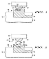
- Testing board 10 has a conventional, multiple-layer structure and is preferably formed from a flouoropolymer for low cost and good planarity. However, other materials including ceramics and organics (such as polyimide) can be used. Testing board 10 and annular contact 16 can both be manufactured using well-known techniques used for forming printed wire boards. In a preferred embodiment, testing board 10 has a plurality of annular contacts 16 disposed on top surface 18, and die 22 has a plurality of conductive bumps 20 to be contacted by contacts 16.
- the degree to which bump 20 is swaged by annular contact 16 is determined by the magnitude of the contacting force used, and it should be noted that the swaging does not require any lateral or rotary motion.
- the contact force has a magnitude sufficiently small so that bump 20 is not deformed beyond the limit suitable for subsequent assembly. For example, if solder bumps are used, the force is sufficiently small that the bumps need not be reflowed to restore their shape following testing by testing board 10.
- bump 20 is swaged to a significant extent into opening 24. If the bump is deformed past the limit suitable for subsequent assembly, it can be re-shaped. For example, with solder bumps this re-shaping can be done by well-known reflowing techniques. Also, it is not necessary that bump 20 contact bottom surface 28 after being swaged, though this can be done if desired. Conventional testing is performed after bump 20 has been swaged.
- opening 24 have a diameter less than the diameter of bump 20.
- a typical diameter for opening 24 when conventional solder bumps are used is about 50 microns.
- annular contact 16 be formed of a material that is harder than that used to form bump 20.
- contact 16 have a modulus of elasticity greater than about 105 kg/m 2 and that bump 20 have a modulus of elasticity less than about 28 kg/m 2 .
- contact 16 preferably has a yield strength at least about four times greater than that of bump 20.
- Contact 16 can, for example, be formed of copper or aluminum and can be optionally plated with a metal layer such as rhodium, palladium, platinum, or a nickel/gold alloy.
- Bump 20 can be a conventional solder bump made from materials such as 95% lead/5% tin, a eutectic solder of 40% lead/60% tin, or other solder materials conventionally used for flip-chip on board (FCOB) and direct chip attach (DCA).
- An advantage of the present invention is that the swaging of bump 20 into contact 16 provides a frictional fit of bump 20 such that die 22 remains substantially fixed in place during testing.
- the magnitude of the frictional force providing this fit varies depending upon the materials used to form bump 20 and contact 16. Specifically, it has been found that if contact 16 is plated with palladium, a solder bump 20 is held with a relatively small frictional force. In contrast, if contact 16 is plated with an alloy of nickel and gold, bump 20 is held in place by a larger frictional force.
- the frictional fitting force will also vary depending on the degree of swaging and the dimensions of opening 24 relative to bump 20.
- the range of acceptable frictional force depends on the number of contacts formed per die (or per wafer if the dies are not singulated) for testing.
- the frictional force should be sufficiently high so the die (or wafer) remains substantially fixed in place during testing, but sufficiently low so the die (or wafer) can be removed from the test board without unacceptable damage to bumps 20.
- edge 26 of contact 16 deforms the surface of bump 20 sufficiently to break through any native oxide layer that is present on the electrically conductive material of bump 20. This ensures a good, uniform electrical contact to all of the typically large number of bumps 20 spread across die 22.
- a further advantage of the present invention observed when swaging a large number of conductive bumps 20 into a like number of annular contacts 16 is an improvement in the compliance of the contact between bumps 20 and contact 16 for the full surface extent of die 22. This additional compliance results in part from the differing degrees of swaging that can occur in each contact 16 across the surface of testing board 10. In other words, by providing a nominal clearance between bump 20 and bottom surface 28, bumps 20 can be swaged to differing degrees depending on the variance of die 22 or testing board 10 from the desired planar or parallel condition.
- bumps 20 As a specific example for the case where many bumps 20 are to be contacted, if surface 21 in a first region of die 22 is a relatively large distance from surface 18 of testing board 10 due to non-planarity, it will be swaged to a relatively small extent. However, if surface 21 in a second region of die 22 is a relatively small distance from surface 18, it will be swaged to a relatively large extent.
- These differing degrees of swaging of bumps 20 provide compliance for non-planarity and/or non-parallelism. Additional compliance can result from the use of a fluoropolymer for testing board 10 because the fluoropolymer itself can be compressed to differing degrees as needed to accommodate non-planarity during the swaging process.
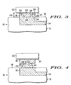
- FIGs. 2 and 3 are cross-sectional side views illustrating an annular contact structure and method according to another embodiment of the present invention for an ideal case of perfect center-on-center alignment. Common reference numerals are used for similar elements.
- FIG. 2 illustrates a swage limit 30 protruding from annular contact 16. Swage limit 30 is used to limit the extent that bump 20 is swaged into opening 24 and can be manufactured using conventional techniques as discussed above for the prior embodiment.
- a first portion 32 of contact 16, which includes limit 30, has an inner diameter greater than the inner diameter of a second portion 34 so that contact 16 has edge 26 as described above for the prior embodiment.
- Annular contact 16 in this embodiment is used substantially as already described above.
- a top surface 38 of swage limit 30 stops any swaging by opening 24 when it contacts die 22.
- the extent of swaging is primarily determined by the dimensions of swage limit 30 rather than the contact force used as for the prior embodiment described above.
- swage limit 30 partly determine the degree of swaging. It is preferable that a swage limit height 40 be substantially equal to a conductive bump height 36 (see FIG. 2) of bump 20. This is preferable in order to provide a uniform and predictable final bump height for bumps swaged during test and burn-in operations, on bumps that are reflowed, or on bumps that are not swaged. A uniform bump height is desirable for reliable assembly of bumped die to circuit boards. Final assembly typically includes underfill operations needing consistently uniform gap heights of the die off of the circuit board surfaces for proper fluid flow.
- Testing board 10 of the present invention provides an improved contact structure compared to the flat-surface contact used in prior testing boards and includes the advantages of self-alignment of bumps 20 and openings 24, good electrical contact to bumps 20 with minimum deformation, and additional tolerance to testing board and semiconductor wafer non-planarity or non-parallelism.
- this annular contact structure provides the benefit of a temporary mechanical attachment between the testing board and the die as supported by the frictional force resulting from the swaged bump surface wiping against the annular contact metal.
Landscapes
- Physics & Mathematics (AREA)
- General Physics & Mathematics (AREA)
- Engineering & Computer Science (AREA)
- Computer Hardware Design (AREA)
- Microelectronics & Electronic Packaging (AREA)
- General Engineering & Computer Science (AREA)
- Testing Of Individual Semiconductor Devices (AREA)
- Measuring Leads Or Probes (AREA)
- Testing Or Measuring Of Semiconductors Or The Like (AREA)
- Structure Of Printed Boards (AREA)
- Contacts (AREA)
Applications Claiming Priority (2)
| Application Number | Priority Date | Filing Date | Title |
|---|---|---|---|
| US49731595A | 1995-07-03 | 1995-07-03 | |
| US497315 | 1995-07-03 |
Publications (3)
| Publication Number | Publication Date |
|---|---|
| EP0752594A2 EP0752594A2 (en) | 1997-01-08 |
| EP0752594A3 EP0752594A3 (en) | 1997-08-06 |
| EP0752594B1 true EP0752594B1 (en) | 2000-05-17 |
Family
ID=23976359
Family Applications (1)
| Application Number | Title | Priority Date | Filing Date |
|---|---|---|---|
| EP96109960A Expired - Lifetime EP0752594B1 (en) | 1995-07-03 | 1996-06-20 | Contact structure for electrically connecting a testing board and die |
Country Status (5)
| Country | Link |
|---|---|
| EP (1) | EP0752594B1 (enExample) |
| JP (1) | JPH0927524A (enExample) |
| KR (1) | KR970007386A (enExample) |
| DE (1) | DE69608355T2 (enExample) |
| TW (1) | TW308724B (enExample) |
Families Citing this family (6)
| Publication number | Priority date | Publication date | Assignee | Title |
|---|---|---|---|---|
| US7078921B2 (en) | 2001-12-25 | 2006-07-18 | Sumitomo Electric Industries, Ltd. | Contact probe |
| KR100436878B1 (ko) * | 2002-06-18 | 2004-06-23 | 건양씨앤이 주식회사 | 강관압입 추진공법시 사용되는 추진강관의 수평유지방법및 그 장치 |
| TWI241669B (en) * | 2003-05-01 | 2005-10-11 | Celerity Res Inc | Planarizing and testing of BGA packages |
| JP4955395B2 (ja) * | 2004-09-06 | 2012-06-20 | 日本電気株式会社 | テストキャリア |
| JP4647700B2 (ja) * | 2009-10-29 | 2011-03-09 | 北陸電気工業株式会社 | プッシュオンスイッチ |
| WO2011071082A1 (ja) * | 2009-12-11 | 2011-06-16 | 日本発條株式会社 | コンタクトプローブ |
Family Cites Families (4)
| Publication number | Priority date | Publication date | Assignee | Title |
|---|---|---|---|---|
| US4975079A (en) * | 1990-02-23 | 1990-12-04 | International Business Machines Corp. | Connector assembly for chip testing |
| GB2247565B (en) * | 1990-08-22 | 1994-07-06 | Gen Electric Co Plc | A method of testing a semiconductor device |
| JP2591348B2 (ja) * | 1993-06-28 | 1997-03-19 | 日本電気株式会社 | 半導体素子の検査治具及び検査方法 |
| GB2279805B (en) * | 1993-07-02 | 1997-09-17 | Plessey Semiconductors Ltd | Bare die testing |
-
1996
- 1996-04-24 TW TW085104899A patent/TW308724B/zh active
- 1996-06-20 EP EP96109960A patent/EP0752594B1/en not_active Expired - Lifetime
- 1996-06-20 DE DE69608355T patent/DE69608355T2/de not_active Expired - Fee Related
- 1996-06-26 JP JP8184232A patent/JPH0927524A/ja active Pending
- 1996-06-28 KR KR1019960024827A patent/KR970007386A/ko not_active Withdrawn
Also Published As
| Publication number | Publication date |
|---|---|
| DE69608355T2 (de) | 2001-01-04 |
| DE69608355D1 (de) | 2000-06-21 |
| EP0752594A3 (en) | 1997-08-06 |
| JPH0927524A (ja) | 1997-01-28 |
| EP0752594A2 (en) | 1997-01-08 |
| TW308724B (enExample) | 1997-06-21 |
| KR970007386A (ko) | 1997-02-21 |
Similar Documents
| Publication | Publication Date | Title |
|---|---|---|
| US7407877B2 (en) | Self-coplanarity bumping shape for flip-chip | |
| US5885849A (en) | Methods of making microelectronic assemblies | |
| US5764486A (en) | Cost effective structure and method for interconnecting a flip chip with a substrate | |
| US6780675B2 (en) | Flip-chip technique for chip assembly | |
| US5686353A (en) | Semiconductor device and manufacturing method thereof | |
| US6984996B2 (en) | Wafer probing that conditions devices for flip-chip bonding | |
| EP1135693B1 (en) | Probe card for probing wafers with raised contact elements | |
| US5726502A (en) | Bumped semiconductor device with alignment features and method for making the same | |
| US6486552B2 (en) | Method and apparatus for testing bumped die | |
| US20070285114A1 (en) | Socket For Making With Electronic Component, Particularly Semiconductor Device With Spring Packaging, For Fixturing, Testing, Burning-In Or Operating Such A Component | |
| JPH0619371B2 (ja) | 電気コネクタ | |
| WO2005065207A2 (en) | Microelectronic packages and methods therefor | |
| US7271611B2 (en) | Method for testing semiconductor components using bonded electrical connections | |
| US6303400B1 (en) | Temporary attach article and method for temporary attach of devices to a substrate | |
| EP0752594B1 (en) | Contact structure for electrically connecting a testing board and die | |
| US5886362A (en) | Method of reflowing solder bumps after probe test | |
| EP1625406A2 (en) | Device probing using a matching device | |
| US20060033515A1 (en) | Test fixture with movable pin contacts | |
| US6831361B2 (en) | Flip chip technique for chip assembly | |
| JPH09172021A (ja) | 半導体装置、半導体装置の製造方法及び実装方法 | |
| JPH10189660A (ja) | フリップチップ接続用回路素子 | |
| Goldstein et al. | Fluxless flip-chip for multichip modules | |
| JPH05340996A (ja) | ベアチップicのバーンイン方法 | |
| JPH0645397A (ja) | 半導体装置の製造方法及び製造装置 |
Legal Events
| Date | Code | Title | Description |
|---|---|---|---|
| PUAI | Public reference made under article 153(3) epc to a published international application that has entered the european phase |
Free format text: ORIGINAL CODE: 0009012 |
|
| AK | Designated contracting states |
Kind code of ref document: A2 Designated state(s): DE FR GB |
|
| PUAL | Search report despatched |
Free format text: ORIGINAL CODE: 0009013 |
|
| AK | Designated contracting states |
Kind code of ref document: A3 Designated state(s): DE FR GB |
|
| 17P | Request for examination filed |
Effective date: 19980206 |
|
| GRAG | Despatch of communication of intention to grant |
Free format text: ORIGINAL CODE: EPIDOS AGRA |
|
| 17Q | First examination report despatched |
Effective date: 19990723 |
|
| GRAG | Despatch of communication of intention to grant |
Free format text: ORIGINAL CODE: EPIDOS AGRA |
|
| GRAH | Despatch of communication of intention to grant a patent |
Free format text: ORIGINAL CODE: EPIDOS IGRA |
|
| GRAH | Despatch of communication of intention to grant a patent |
Free format text: ORIGINAL CODE: EPIDOS IGRA |
|
| GRAA | (expected) grant |
Free format text: ORIGINAL CODE: 0009210 |
|
| AK | Designated contracting states |
Kind code of ref document: B1 Designated state(s): DE FR GB |
|
| REF | Corresponds to: |
Ref document number: 69608355 Country of ref document: DE Date of ref document: 20000621 |
|
| ET | Fr: translation filed | ||
| PLBE | No opposition filed within time limit |
Free format text: ORIGINAL CODE: 0009261 |
|
| STAA | Information on the status of an ep patent application or granted ep patent |
Free format text: STATUS: NO OPPOSITION FILED WITHIN TIME LIMIT |
|
| 26N | No opposition filed | ||
| REG | Reference to a national code |
Ref country code: GB Ref legal event code: IF02 |
|
| REG | Reference to a national code |
Ref country code: GB Ref legal event code: 732E |
|
| PGFP | Annual fee paid to national office [announced via postgrant information from national office to epo] |
Ref country code: GB Payment date: 20050506 Year of fee payment: 10 |
|
| PGFP | Annual fee paid to national office [announced via postgrant information from national office to epo] |
Ref country code: FR Payment date: 20050602 Year of fee payment: 10 |
|
| PGFP | Annual fee paid to national office [announced via postgrant information from national office to epo] |
Ref country code: DE Payment date: 20050630 Year of fee payment: 10 |
|
| PG25 | Lapsed in a contracting state [announced via postgrant information from national office to epo] |
Ref country code: GB Free format text: LAPSE BECAUSE OF NON-PAYMENT OF DUE FEES Effective date: 20060620 |
|
| PG25 | Lapsed in a contracting state [announced via postgrant information from national office to epo] |
Ref country code: DE Free format text: LAPSE BECAUSE OF NON-PAYMENT OF DUE FEES Effective date: 20070103 |
|
| GBPC | Gb: european patent ceased through non-payment of renewal fee |
Effective date: 20060620 |
|
| REG | Reference to a national code |
Ref country code: FR Ref legal event code: ST Effective date: 20070228 |
|
| PG25 | Lapsed in a contracting state [announced via postgrant information from national office to epo] |
Ref country code: FR Free format text: LAPSE BECAUSE OF NON-PAYMENT OF DUE FEES Effective date: 20060630 |