EP0747713B1 - Schaltungsanordnung zum Erfassen des Laststroms eines Leistungshalbleiterbauelementes mit source- oder drainseitiger Last - Google Patents
Schaltungsanordnung zum Erfassen des Laststroms eines Leistungshalbleiterbauelementes mit source- oder drainseitiger Last Download PDFInfo
- Publication number
- EP0747713B1 EP0747713B1 EP96108434A EP96108434A EP0747713B1 EP 0747713 B1 EP0747713 B1 EP 0747713B1 EP 96108434 A EP96108434 A EP 96108434A EP 96108434 A EP96108434 A EP 96108434A EP 0747713 B1 EP0747713 B1 EP 0747713B1
- Authority
- EP
- European Patent Office
- Prior art keywords
- semiconductor component
- resistor
- mosfet
- source
- input
- Prior art date
- Legal status (The legal status is an assumption and is not a legal conclusion. Google has not performed a legal analysis and makes no representation as to the accuracy of the status listed.)
- Expired - Lifetime
Links
Images
Classifications
-
- G—PHYSICS
- G01—MEASURING; TESTING
- G01R—MEASURING ELECTRIC VARIABLES; MEASURING MAGNETIC VARIABLES
- G01R19/00—Arrangements for measuring currents or voltages or for indicating presence or sign thereof
-
- G—PHYSICS
- G05—CONTROLLING; REGULATING
- G05F—SYSTEMS FOR REGULATING ELECTRIC OR MAGNETIC VARIABLES
- G05F3/00—Non-retroactive systems for regulating electric variables by using an uncontrolled element, or an uncontrolled combination of elements, such element or such combination having self-regulating properties
- G05F3/02—Regulating voltage or current
- G05F3/08—Regulating voltage or current wherein the variable is DC
- G05F3/10—Regulating voltage or current wherein the variable is DC using uncontrolled devices with non-linear characteristics
- G05F3/16—Regulating voltage or current wherein the variable is DC using uncontrolled devices with non-linear characteristics being semiconductor devices
- G05F3/20—Regulating voltage or current wherein the variable is DC using uncontrolled devices with non-linear characteristics being semiconductor devices using diode- transistor combinations
- G05F3/24—Regulating voltage or current wherein the variable is DC using uncontrolled devices with non-linear characteristics being semiconductor devices using diode- transistor combinations wherein the transistors are of the field-effect type only
-
- G—PHYSICS
- G01—MEASURING; TESTING
- G01R—MEASURING ELECTRIC VARIABLES; MEASURING MAGNETIC VARIABLES
- G01R1/00—Details of instruments or arrangements of the types included in groups G01R5/00 - G01R13/00 and G01R31/00
- G01R1/20—Modifications of basic electric elements for use in electric measuring instruments; Structural combinations of such elements with such instruments
- G01R1/203—Resistors used for electric measuring, e.g. decade resistors standards, resistors for comparators, series resistors, shunts
-
- G—PHYSICS
- G01—MEASURING; TESTING
- G01R—MEASURING ELECTRIC VARIABLES; MEASURING MAGNETIC VARIABLES
- G01R19/00—Arrangements for measuring currents or voltages or for indicating presence or sign thereof
- G01R19/0092—Measuring current only
-
- H—ELECTRICITY
- H03—ELECTRONIC CIRCUITRY
- H03K—PULSE TECHNIQUE
- H03K17/00—Electronic switching or gating, i.e. not by contact-making and –breaking
- H03K17/14—Modifications for compensating variations of physical values, e.g. of temperature
- H03K17/145—Modifications for compensating variations of physical values, e.g. of temperature in field-effect transistor switches
-
- H—ELECTRICITY
- H03—ELECTRONIC CIRCUITRY
- H03K—PULSE TECHNIQUE
- H03K2217/00—Indexing scheme related to electronic switching or gating, i.e. not by contact-making or -breaking covered by H03K17/00
- H03K2217/0027—Measuring means of, e.g. currents through or voltages across the switch
Definitions
- the prerequisite is that the measuring resistor is matched to the load. For a different load, therefore, either the measuring resistor must be changed or the voltage-detecting evaluation logic must be changed.
- US Pat. No. 4,885,477 describes a circuit arrangement with a power MOSFET and a sense FET in which a further MOSFET, which serves as a controllable resistor, is connected in series with the measuring resistor.
- This further MOSFET is driven by a differential amplifier such that the drain-source voltage of the sense FET and the drain-source voltage of the power MOSFET assume approximately equal values.
- the offset voltage of the differential amplifier produces a control error and there remains a certain difference between the drain-source voltages of sense FET and power MOSFET.
- a similar circuit is disclosed in EP 0 227 149.
- the invention has the object of developing a circuit of the type mentioned so that this control error is reduced. In addition, it should be usable for the most common case of the high-side switch.
- the resistor is connected on the one hand to a terminal lying at a fixed potential and on the other hand connected via a controllable resistor to the source terminal of the other semiconductor device and the current of the other semiconductor device is adjusted by the controllable resistor such that the drain-source voltages of both semiconductor devices are equal to each other ,
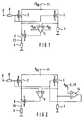
- the circuit of Figure 1 includes a power MOSFET 1, the source side of a load 4 is connected in series. It thus constitutes a high-side switch.
- the circuit also contains a further MOSFET 2.
- the drain terminals D of both MOSFETs are connected together, as are their gate terminals. Their source connections are disconnected.
- a controllable resistor 6 is connected.
- the controllable resistor is connected via a terminal 10 to a measuring resistor 5.
- the other terminal of the measuring resistor 5 is connected to a fixed potential, preferably to ground. This mass may, but need not be, identical to that at which the load 4 is located.
- the controllable resistor 6 is expediently designed as a MOSFET. Then, its source is connected to the sense resistor 5 and its drain connected to the source of the MOSFET 2. It is of the reverse channel type as the MOSFET 2. The gate of the MOSFET 6 is connected to the output of a differential amplifier 3. This has two inputs, of which the negative input to the source of the MOSFET 2 and the positive input to the source of the power MOSFET 1 is connected.
- the entire assembly is at an operating voltage + V bb applied between a terminal 11 and ground.
- the terminal 11 is connected to the drains of the MOSFETs 1 and 2.
- the gate terminals of both MOSFETs are connected via a resistor 8 to an input 9, to which, for example via a pump circuit, a control voltage can be applied.
- the power MOSFET 1 and the further MOSFET 2 is turned on. It flows a load current through the load 4.
- the controllable resistor 6 and the measuring resistor 5 also flows a current.
- a voltage is applied, which is applied to the negative or positive input of the differential amplifier 3. Depending on the difference of these voltages occurs at the output of 3, a voltage that controls the MOSFET 6.
- the source-drain voltage at the MOSFET 2 is greater than that at the MOSFET 1. Then occurs at the input of the differential amplifier 3, a voltage which controls the MOSFET 6 in a region of higher resistance. The current through the MOSFET 2 is thereby reduced, increasing its drain-source voltage. The current through MOSFET 2 is now regulated until the difference of the input voltages is zero, i. until the drain-source voltages of the MOSFETs 1 and 2 are the same. This means that in the adjusted, stationary state through the measuring resistor 5, a current flows, which is always fixedly proportional to the load current, regardless of the size of the load 4. Thus, in the course of operation, the load 4 changes, e.g.
- the drain-source voltage on the power MOSFET 1 increases or decreases and thus the variable resistor 6 is controlled in the direction of lower or higher resistance until the voltage difference at the input of the amplifier 3 is zero.
- the I D / U DS characteristics of MOSFET 1 and 2 are similar to each other. That is, for each voltage value U DS through the other FET 2, a current flows, which is a fixed fraction of the load current. This current generated at the resistor 5 is a reference to ground, the load current proportional voltage that can be tapped at the terminal 10.
- the similarity can be easily achieved in that, as mentioned above, the MOSFET 2 is formed by some cells of the power MOSFET 1.
- the ratio may be 10: 10000, for example.
- the circuit arrangement according to the invention according to Figure 2 differs from that of Figure 1 by an additional differential amplifier 14, whose first input is connected to the source terminal of the power MOSFET 1. At the other input of the differential amplifier 14 is a fixed voltage. The output of 14 is connected to the gates of MOSFETs 1 and 2.
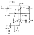
- the embodiment of Figure 3 is compared to that of Figure 1 supplemented by some components.
- the negative input of the amplifier 3 is connected via a diode 15 to the terminal 11 and a power source 18 to ground.
- the other output is connected via a diode 16 to the terminal 11 and a power source 20 to ground.
- the negative input is also connected via a diode 17 to the source of the MOSFET 2, the positive input via a diode 19 to the source of the power MOSFET 1.
- the diodes and current sources are used to set the amplifier 3, the correct operating point. All diodes can be designed as MOS diodes, the current sources can be realized as a current mirror circuit or as a depletion MOSFET.
- a resistor 21 may be connected, whose connected to the gate terminal of 6 terminal is connected to a capacitor 22. The other terminal of the capacitor is grounded. This RC combination counteracts the tendency of the amplifier 3 to oscillate.
- the amplifier 3 is expediently an operational amplifier.
- the circuit according to the invention can be operated substantially independent of temperature, if the measuring resistor 5 itself is independent of temperature or little temperature dependent. This can e.g. be achieved in that the measuring resistor 5 is made of polysilicon or is designed as a temperature-compensated resistor.
- the circuit was explained using a high-side switch. However, it is also applicable to a low-side switch.
- the load 4 is on the drain side of the two MOSFETs, while the controllable switch 6 and the measuring resistor 5 remains connected to the source side of the MOSFET 2.
Landscapes
- Physics & Mathematics (AREA)
- Engineering & Computer Science (AREA)
- General Physics & Mathematics (AREA)
- Microelectronics & Electronic Packaging (AREA)
- Nonlinear Science (AREA)
- Electromagnetism (AREA)
- Radar, Positioning & Navigation (AREA)
- Automation & Control Theory (AREA)
- Amplifiers (AREA)
- Measurement Of Current Or Voltage (AREA)
- Testing Of Individual Semiconductor Devices (AREA)
- Control Of Voltage And Current In General (AREA)
Description
- Die Erfindung bezieht sich auf eine Schaltungsanordnung zum Erfassen des Laststroms eines durch Feldeffekt steuerbaren Leistungs-Halbleiterbauelements, mit den Merkmalen:
- einem weiteren durch Feldeffekt steuerbaren Halbleiterbauelement,
- die Drainanschlüsse und Gateanschlüsse beider Halbleiterbauelemente sind jeweils miteinander verbunden,
- durch das weitere Halbleiterbauelement fließt ein Bruchteil des Laststroms,
- einem dem weiteren Halbleiterbauelement in Reihe geschalteten Widerstand, an dem eine dem Laststrom proportionale Spannung abgreifbar ist.
- Eine solche Schaltungsanordnung ist z.B. in dem Artikel "Surviving Short Circuits" von R.Frank und A.Pshaenich, Machine Design, March 8, 1990, Seiten 89 bis 96 beschrieben worden. In diesem Artikel ist das Prinzip dargestellt, daß der Laststrom eines Leistungs-MOSFET dadurch erfaßt werden kann, daß dem Leistungs-MOSFET ein ähnlicher, von der Fläche her kleinerer MOSFET parallel geschaltet und diesem kleineren MOSFET, dem sogenannten "Sense"-FET, sourceseitig ein Meßwiderstand in Reihe geschaltet wird. Ist der Leistungs-FET drainseitig mit einer Last verbunden, so fließt durch den weiteren FET ein Strom, der dem Laststrom etwa proportional ist. Der Proportionalitätsfaktor hängt dabei vom Verhältnis der stromführenden Flächen des Sense-FET zu der des Leistungs-FET ab. Fließt durch die Last und damit durch den Leistungs-FET ein Laststrom, so fließt damit ein dem Laststrom etwa proportionaler Teil durch den Sense-FET und den Meßwiderstand. Am Meßwiderstand kann dann eine dem Laststrom etwa proportionale Spannung abgegriffen werden.
- Voraussetzung ist dabei, dass der Messwiderstand auf die Last abgestimmt ist. Bei einer anderen Last muss daher entweder der Messwiderstand geändert werden oder die die Spannung erfassende Auswertelogik.
- Die US-Patentschrift US 4,885,477 beschreibt eine Schaltungsanordnung mit einem Leistungs-MOSFET und einem Sense-FET, bei dem in Serie zum Messwiderstand ein weiterer MOSFET, welcher als steuerbarer Widerstand dient, geschalten ist. Dieser weitere MOSFET wird von einem Differenzverstärker derart angesteuert, dass die Drain-Sourcespannung des Sense-FET und die Drain-Sourcespannung des Leistungs-MOSFET annähernd gleiche Werte annehmen. Durch die Offset-Spannung des Differenzverstärkers entsteht ein Regelfehler und es bleibt eine gewisse Differenz zwischen den Drain-Sourcespannungen von Sense-FET und Leistungs-MOSFET. Eine ähnliche Schaltung ist in EP 0 227 149 offenbart.
- Der Erfindung liegt die Aufgabe zugrunde, eine Schaltung der erwähnten Gattung so weiterzubilden, dass dieser Regelfehler reduziert wird. Außerdem soll sie für den meist vorkommenden Fall des High-Side-Schalters verwendbar sein.
- Diese Aufgabe wird durch eine Schaltungsanordnung gemäß Patentanspruch 1 gelöst, vorteilhafte Weiterentwicklungen finden sich in den Unteransprüchen.
Der Widerstand ist einerseits mit einem auf festem Potential liegenden Anschluss verbunden und andererseits über einen steuerbaren Widerstand mit dem Sourceanschluss des weiteren Halbleiterbauelementes verbunden und der Strom des weiteren Halbleiterbauelementes wird durch den steuerbaren Widerstand derart eingestellt wird, dass die Drain-Sourcespannungen beider Halbleiterbauelemente einander gleich sind. - Wird die Schaltungsanordnung nicht mit Leistungs-MOSFET sondern mit IGBT betrieben, so ist der Begriff "Source" durch "Emitter" zu ersetzen.
- Die Erfindung wird in Verbindung mit den Figuren 1 bis 3 näher erläutert. Es zeigen:
- Figur 1
- den prinzipiellen Aufbau der Schaltungsanordnung,
- Figur 2
- eine erweiterte Schaltungsanordnung gemäß der Erfindung und
- Figur 3
- eine Anordnung, die gegenüber der nach Figur 1 durch verschiedene Komponenten ergänzt ist.
- Die Schaltung nach Figur 1 enthält einen Leistungs-MOSFET 1, dem sourceseitig eine Last 4 in Reihe geschaltet ist. Er stellt damit einen High-Side-Schalter dar. Die Schaltung enthält außerdem einen weiteren MOSFET 2. Dieser bildet den erwähnten Sense-FET und ist im allgemeinen durch einige Zellen des Leistungs-MOSFET 1 gebildet. Er kann z.B. 10 Zellen umfassen, während der Leistungs-MOSFET 1 10000 Zellen hat. Die Drainanschlüsse D beider MOSFET sind miteinander verbunden, ebenso ihre Gateanschlüsse. Ihre Sourceanschlüsse sind getrennt. Mit dem Sourceanschluß des MOSFET 2 ist ein steuerbarer Widerstand 6 angeschlossen. Der steuerbare Widerstand ist andererseits über einen Anschluß 10 mit einem Meßwiderstand 5 verbunden. Der andere Anschluß des Meßwiderstandes 5 liegt an einem festen Potential, vorzugsweise an Masse. Diese Masse kann, muß jedoch jedoch nicht derjenigen identisch sein, an der die Last 4 liegt.
- Der steuerbare Widerstand 6 ist zweckmäßigerweise als MOSFET ausgebildet. Dann ist sein Sourceanschluß mit dem Meßwiderstand 5 verbunden und sein Drainanschluß mit dem Sourceanschluß des MOSFET 2. Er ist vom umgekehrten Kanaltyp wie der MOSFET 2. Der Gateanschluß des MOSFET 6 ist mit dem Ausgang eines Differenzverstärkers 3 verbunden. Dieser hat zwei Eingänge, von denen der negative Eingang mit dem Sourceanschluß des MOSFET 2 und der positive Eingang mit dem Sourceanschluß des Leistungs-MOSFET 1 verbunden ist.
- Die gesamte Anordnung liegt an einer Betriebsspannung +Vbb, die zwischen einem Anschluß 11 und Masse angelegt wird. Der Anschluß 11 ist mit den Drainanschlüssen der MOSFET 1 und 2 verbunden. Die Gateanschlüsse beider MOSFET sind über einen Widerstand 8 mit einem Eingang 9 verbunden, an den, z.B. über eine Pumpschaltung eine Steuerspannung angelegt werden kann.
- Wird eine Steuerspannung am Eingang 9 angelegt, so wird der Leistungs-MOSFET 1 und der weitere MOSFET 2 leitend gesteuert. Es fließt ein Laststrom durch die Last 4. Durch den MOSFET 2, den steuerbaren Widerstand 6 und den Meßwiderstand 5 fließt ebenfalls ein Strom. An den Sourceanschlüssen der MOSFET 1 und 2 stellt sich jeweils eine Spannung ein, die am negativen bzw. positiven Eingang des Differenzverstärkers 3 anliegt. Abhängig von der Differenz dieser Spannungen tritt am Ausgang von 3 eine Spannung auf, die den MOSFET 6 steuert.
- Es sei zunächst angenommen, daß die Source-Drainspannung am MOSFET 2 größer ist als die am MOSFET 1. Dann tritt am Eingang des Differenzverstärkers 3 eine Spannung auf, die den MOSFET 6 in einen Bereich höheren Widerstandes steuert. Der Strom durch den MOSFET 2 wird dadurch verringert, wodurch seine Drain-Sourcespannung steigt. Der Strom durch den MOSFET 2 wird nun so lange geregelt, bis die Differenz der Eingangsspannungen Null ist, d.h. bis die Drain-Sourcespannungen der MOSFET 1 und 2 gleich sind. Das bedeutet, daß im eingeregelten, stationären Zustand durch den Meßwiderstand 5 ein Strom fließt, der dem Laststrom unabhängig von der Größe der Last 4 immer fest proportional ist. Ändert sich also im Lauf des Betriebes die Last 4 z.B. durch einen teilweisen Kurzschluß oder durch den Ausfall einiger parallelgeschalteter Lasten, so erhöht bzw. verringert sich die Drain-Sourcespannung am Leistungs-MOSFET 1 und damit wird der veränderbare Widerstand 6 in Richtung geringeren bzw. höheren Widerstandes gesteuert, bis die Spannungsdifferenz am Eingang des Verstärkers 3 Null ist.
- Voraussetzung für die feste Proportionalität ist, daß die ID/UDS-Kennlinien der MOSFET 1 und 2 einander ähnlich sind. D.h., daß für jeden Spannungswert UDS durch den weiteren FET 2 ein Strom fließt, der einem festen Bruchteil des Laststroms beträgt. Dieser Strom erzeugt am Widerstand 5 eine auf Masse bezogene, dem Laststrom proportionale Spannung, die am Anschluß 10 abgegriffen werden kann. Die Ähnlichkeit läßt sich ohne weiteres dadurch erzielen, daß, wie eingangs erwähnt, der MOSFET 2 durch einige Zellen des Leistungs-MOSFET 1 gebildet ist. Das Verhältnis kann z.B. 10:10000 sein.
- Sind die Kennlinien einander nicht ähnlich, tritt ein vom Laststrom abhängiger Regelfehler auf.
- Die erfindungsgemäße Schaltungsanordnung nach Figur 2 unterscheidet sich von der nach Figur 1 durch einen zusätzlichen Differenzverstärker 14, dessen erster Eingang mit dem Sourceanschluß des Leistungs-MOSFET 1 verbunden ist. Am anderen Eingang des Differenzverstärkers 14 liegt eine feste Spannung an. Der Ausgang von 14 ist mit den Gateanschlüssen der MOSFET 1 und 2 verbunden. Der zusätzliche Differenzverstärker 14 hat den Zweck, die Drain-Sourcespannung des MOSFET 1 auf einen Wert einzustellen, der höher ist als die Offset-Spannung des Differenzverstärkers 3. Beträgt die Offset-Spannung z.B. 5 mV, so kann die am zweiten Eingang des Verstärkers 14 liegende Spannung z.B. Vbb-0,1 V sein. Damit wird die Drain-Sourcespannung des MOSFET auf 0,1 V eingestellt. Bei der erwähnten Größe der Offset-Spannung beträgt der Regelfehler dann nur 5/100 mV = 5%. Die Erhöhung der Drain-Sourcespannung am MOSFET 1 um z.B. 0,1 V erhöht den Durchlaßwiderstand des Leistungs-MOSFET nur unerheblich. Damit ist die Erhöhung der Verluste im Leistungs-MOSFET 1 vernachlässigbar gering.
- Das Ausführungsbeispiel nach Figur 3 ist gegenüber dem nach Figur 1 um einige Bauteile ergänzt. So ist der negative Eingang des Verstärkers 3 über eine Diode 15 mit dem Anschluß 11 und über eine Stromquelle 18 mit Masse verbunden. Der andere Ausgang ist über eine Diode 16 mit dem Anschluß 11 und über eine Stromquelle 20 mit Masse verbunden. Der negative Eingang ist außerdem über eine Diode 17 mit dem Sourceanschluß des MOSFET 2 verbunden, der positive Eingang über eine Diode 19 mit dem Sourceanschluß des Leistungs-MOSFET 1. Die Dioden und Stromquellen dienen dazu, dem Verstärker 3 den richtigen Arbeitspunkt einzustellen. Alle Dioden können als MOS-Dioden ausgeführt sein, die Stromquellen können als Stromspiegelschaltung oder als Depletion-MOSFET realisiert werden.
- Zwischen dem Ausgang des Verstärkers 3 und dem Gateanschluß des MOSFET 6 kann ein Widerstand 21 angeschlossen sein, dessen mit dem Gateanschluß von 6 verbundener Anschluß mit einem Kondensator 22 verbunden ist. Der andere Anschluß des Kondensators liegt auf Masse. Diese RC-Kombination wirkt der Schwingneigung des Verstärkers 3 entgegen. Der Verstärker 3 ist zweckmäßigerweise ein Operationsverstärker.
- Die erfindungsgemäße Schaltung läßt sich im wesentlichen temperaturunabhängig betreiben, wenn der Meßwiderstand 5 selbst temperaturunabhängig oder wenig temperaturabhängig ist. Dies kann z.B. dadurch erreicht werden, daß der Meßwiderstand 5 aus Polysilizium besteht oder als temperaturkompensierter Widerstand ausgeführt ist.
- Die Schaltung wurde anhand eines High-Side-Schalters erläutert. Sie ist jedoch auch für einen Low-Side-Schalter anwendbar. Hier befindet sich die Last 4 auf der Drainseite der beiden MOSFET, während der steuerbare Schalter 6 und der Meßwiderstand 5 auf der Sourceseite des MOSFET 2 angeschlossen bleibt.
Claims (5)
- Schaltungsanordnung zum Erfassen des Laststromes eines durch Feldeffekt steuerbaren Leistungs-Halbleiterbauelements (1), mit den Merkmalen:- einem weiteren durch Feldeffekt steuerbaren Halbleiterbauelement (2),- die Drainanschlüsse und Gateanschlüsse beider Halbleiterbauelemente sind jeweils miteinander verbunden,- durch das weitere Hableiterbauelement fliesst ein Bruchteil des Laststroms,- einem dem weiteren Halbleiterbauelement in Reihe geschalteten Widerstand (5), an dem eine dem Laststrom proportionale Spannung abgreifbar ist,wobei- der Widerstand (5) einerseits mit einem auf festem Potential liegenden Anschluss verbunden ist und andererseits über einen steuerbaren Widerstand (6) mit dem Sourceanschluss des weiteren Halbleiterbauelements (2), und wobei- der Strom des weiteren Halbleiterbauelementes (2) durch den steuerbaren Widerstand (6) derart eingestellt wird, dass die Drain-Sourcespannungen beider Halbleiterbauelemente (1, 2) einander gleich sind, und wobei- der steuerbare Widerstand (6) ein MOSFET ist, dessen Steuereingang mit dem Ausgang eines ersten Differenzverstärkers (3) verbunden ist, dessen erster Eingang mit dem Sourceanschluss des Leistungs-Halbleiterbauelements (1) und dessen zweiter Eingang mit dem Sourceanschluss des weiteren Halbleiterbauelements (2) verbunden ist,dadurch gekennzeichnet, dass der Sourceanschluss des Leistungs-Halbleiterbauelements (1) mit dem ersten Eingang eines zweiten Differenzverstärkers (14) verbunden ist, an dessen zweitem Eingang eine Spannung anlegbar ist, die größer ist als die Offset-Spannung des ersten Differenzverstärkers (3).
- Schaltungsanordnung nach Anspruch 1,
dadurch gekennzeichnet, dass der Differenzverstärker (3) ein Operationsverstärker ist. - Schaltungsanordnung nach Anspruch 1,
dadurch gekennzeichnet, dass das feste Potential Massepotential ist. - Schaltungsanordnung nach einem der Ansprüche 1 bis 3,
dadurch gekennzeichnet, dass die bei den Halbleiterbauelemente (1, 2) einander ähnliche ID/UDS-Kennlinien haben. - Schaltungsanordnung nach einem der Ansprüche 1 bis 4,
dadurch gekennzeichnet, dass das Leistungs-Halbleiterbauelement (1) und das weitere Halbleiterbauelement (2) aus einer Vielzahl von auf einem einzigen Chip integrierten Zellen besteht.
Applications Claiming Priority (2)
| Application Number | Priority Date | Filing Date | Title |
|---|---|---|---|
| DE19520735A DE19520735C2 (de) | 1995-06-07 | 1995-06-07 | Schaltungsanordnung zum Erfassen des Laststroms eines Leistungs-Halbleiterbauelementes mit sourceseitiger Last |
| DE19520735 | 1995-06-07 |
Publications (3)
| Publication Number | Publication Date |
|---|---|
| EP0747713A2 EP0747713A2 (de) | 1996-12-11 |
| EP0747713A3 EP0747713A3 (de) | 1998-01-07 |
| EP0747713B1 true EP0747713B1 (de) | 2006-07-12 |
Family
ID=7763807
Family Applications (1)
| Application Number | Title | Priority Date | Filing Date |
|---|---|---|---|
| EP96108434A Expired - Lifetime EP0747713B1 (de) | 1995-06-07 | 1996-05-28 | Schaltungsanordnung zum Erfassen des Laststroms eines Leistungshalbleiterbauelementes mit source- oder drainseitiger Last |
Country Status (5)
| Country | Link |
|---|---|
| US (1) | US5815027A (de) |
| EP (1) | EP0747713B1 (de) |
| JP (1) | JPH08334534A (de) |
| KR (1) | KR970002339A (de) |
| DE (2) | DE19520735C2 (de) |
Families Citing this family (58)
| Publication number | Priority date | Publication date | Assignee | Title |
|---|---|---|---|---|
| DE19706946C2 (de) * | 1997-02-21 | 2000-06-21 | Daimler Chrysler Ag | Battierüberwachungseinheit |
| ITMI981217A1 (it) * | 1997-06-05 | 1999-12-02 | Denso Corp | Struttura perfezionata per un circuito di misura di corrente |
| DE19812920C2 (de) * | 1998-03-24 | 2000-09-07 | Siemens Ag | Schaltungsanordnung zur Steuerung und Erfassung des Laststromes durch eine Last |
| KR100702810B1 (ko) * | 1998-06-09 | 2007-04-03 | 코닌클리케 필립스 일렉트로닉스 엔.브이. | 전류 측정 장치와 전류 측정 장치를 사용하는 전화 단말기 |
| DE19830356C1 (de) * | 1998-07-07 | 1999-11-11 | Siemens Ag | Verfahren zum Abgleichen eines Widerstands in einer integrierten Schaltung und Vorrichtung zur Durchführung dieses Verfahrens |
| DE19838657B4 (de) * | 1998-08-25 | 2008-01-24 | Infineon Technologies Ag | Schaltungsanordnung zum Erfassen des Laststromes eines Leistungs-Feldeffekt-Halbleiterbauelementes |
| JP3628576B2 (ja) * | 1999-02-14 | 2005-03-16 | 矢崎総業株式会社 | 微少電流検出装置 |
| GB9908285D0 (en) * | 1999-04-13 | 1999-06-02 | Koninkl Philips Electronics Nv | A power switching circuit |
| DE10019240A1 (de) * | 2000-04-18 | 2001-10-31 | Fujitsu Siemens Computers Gmbh | Schaltungsanordnung zur Messung der Stromaufnahme einer transistorgesteuerten Last |
| DE10057486A1 (de) | 2000-06-15 | 2016-10-13 | Continental Teves Ag & Co. Ohg | Verfahren und Schaltungsanordnung zur Erkennung eines Defekts von Halbleiterschaftelementen und dessen/deren Verwendung in Kraftfahrzeugen, insbesondere Bremskraft- und Fahrdynamikreglern |
| DE10032260B4 (de) * | 2000-07-03 | 2004-04-29 | Texas Instruments Deutschland Gmbh | Schaltungsanordnung zur Verdoppelung der Spannung einer Batterie |
| ATE294397T1 (de) * | 2000-10-13 | 2005-05-15 | Primarion Inc | System und verfahren zur strommessung |
| US6407532B1 (en) * | 2000-12-29 | 2002-06-18 | Nokia Mobile Phones, Ltd. | Method and apparatus for measuring battery charge and discharge current |
| DE10195897D2 (de) | 2001-01-23 | 2003-12-18 | Continental Teves Ag & Co Ohg | Schaltungsanordnung und Verfahren zur Messung des Stroms in Kraftfahrzeugbremssystemen |
| DE10103920A1 (de) * | 2001-01-30 | 2002-08-22 | Infineon Technologies Ag | Schaltungsanordnung mit einem Lasttransistor und einer Strommessanordnung |
| DE10120524B4 (de) * | 2001-04-26 | 2015-08-20 | Infineon Technologies Ag | Vorrichtung zur Ermittlung des Stromes durch ein Leistungs-Halbleiterbauelement |
| ATE495454T1 (de) * | 2002-04-02 | 2011-01-15 | Dialog Semiconductor Gmbh | Leistungsschalter mit stromabfühlschaltung |
| DE10240914B4 (de) | 2002-09-04 | 2007-01-25 | Infineon Technologies Ag | Schaltungsanordnung mit einem Lasttransistor und einer Strommessanordnung und Verfahren zur Ermittlung des Laststroms eines Lasttransistors sowie Verwendung eines Halbleiterbauelements |
| GB0312237D0 (en) * | 2003-05-29 | 2003-07-02 | Koninkl Philips Electronics Nv | Undercurrent sense arrangement and method |
| DE102005009544B4 (de) * | 2005-03-02 | 2008-09-04 | Infineon Technologies Ag | Bauelementanordnung mit einem Lasttransistor und einem Messtransistor |
| DE102005010337B4 (de) | 2005-03-07 | 2013-02-21 | Infineon Technologies Austria Ag | Bauelementanordnung mit einem Bipolartransistor und einem Lastunterbrechungsdetektor |
| DE102005019955A1 (de) * | 2005-04-29 | 2006-11-02 | Infineon Technologies Ag | Variables Ansteuermodul zur Ansteuerung einer Last |
| JP2008543208A (ja) * | 2005-06-01 | 2008-11-27 | エヌエックスピー ビー ヴィ | 負荷電流決定回路及び方法 |
| GB2431739A (en) * | 2005-10-27 | 2007-05-02 | Wolfson Microelectronics Plc | Switch current sensing circuit |
| JP4842614B2 (ja) * | 2005-10-27 | 2011-12-21 | ルネサスエレクトロニクス株式会社 | 電流検出回路 |
| KR101221799B1 (ko) * | 2005-11-21 | 2013-01-14 | 페어차일드코리아반도체 주식회사 | 전류감지 회로 및 이를 구비한 부스트 컨버터 |
| DE102006037554B3 (de) * | 2006-08-10 | 2007-11-22 | Infineon Technologies Ag | Verfahren zur Einstellung eines Bezugspotentials eines Stromfühlers und Anordnung zur Bestimmung des Bezugspotentials einer Leistungshalbleitereinrichtung |
| JP2009075957A (ja) * | 2007-09-21 | 2009-04-09 | Renesas Technology Corp | 電源回路および半導体装置 |
| DE102008055696A1 (de) | 2008-01-25 | 2009-07-30 | Continental Teves Ag & Co. Ohg | Elektronische Schaltungseinrichtung zur Erfassung eines Detektionselementstroms und/oder einer Temperatur in diesem Detektionselement |
| JP5044448B2 (ja) | 2008-03-03 | 2012-10-10 | ルネサスエレクトロニクス株式会社 | 電源スイッチ回路 |
| US20090295369A1 (en) * | 2008-06-02 | 2009-12-03 | Yang Doris | Current sensing circuit |
| JP5171406B2 (ja) * | 2008-06-05 | 2013-03-27 | 矢崎総業株式会社 | 負荷回路の過電流保護装置 |
| DE102008044634B4 (de) | 2008-08-27 | 2017-12-21 | Fraunhofer-Gesellschaft zur Förderung der angewandten Forschung e.V. | Vorrichtung und Verfahren zum Erfassen eines Durchschnittswerts eines geschalteten Stromes in einer Spule |
| US7911260B2 (en) | 2009-02-02 | 2011-03-22 | Infineon Technologies Ag | Current control circuits |
| US8643068B2 (en) * | 2009-03-12 | 2014-02-04 | Infineon Technologies Ag | Integrated circuit having field effect transistors and manufacturing method |
| DE102009001899B4 (de) | 2009-03-26 | 2024-01-18 | Robert Bosch Gmbh | Messen eines Laststroms eines Unterbrechers |
| US20110185179A1 (en) * | 2009-08-26 | 2011-07-28 | Viswanathan Swaminathan | System And Method For Digital Rights Management With A Lightweight Digital Watermarking Component |
| WO2012137670A1 (ja) * | 2011-04-05 | 2012-10-11 | ルネサスエレクトロニクス株式会社 | 負荷電流検出回路 |
| US8493136B2 (en) * | 2011-04-08 | 2013-07-23 | Icera Inc. | Driver circuit and a mixer circuit receiving a signal from the driver circuit |
| EP2746890B1 (de) * | 2012-12-19 | 2017-09-27 | Nxp B.V. | Stromüberwachungsschaltungen und -verfahren |
| WO2014121484A1 (en) * | 2013-02-07 | 2014-08-14 | Texas Instruments Incorporated | Bi-directional input, bi-directional output, lossless current sensing scheme with temperature compensation |
| US9853533B2 (en) * | 2013-04-25 | 2017-12-26 | Infineon Technologies Austria Ag | Circuit arrangement and method for reproducing a current |
| US9360879B2 (en) * | 2014-04-28 | 2016-06-07 | Microsemi Corp.-Analog Mixed Signal Group, Ltd. | Sense current generation apparatus and method |
| US9829387B2 (en) | 2014-10-28 | 2017-11-28 | Infineon Technologies Austria Ag | System and method for temperature sensing |
| JP2016200570A (ja) | 2015-04-14 | 2016-12-01 | ルネサスエレクトロニクス株式会社 | 半導体装置の電流検出方法および半導体装置 |
| JP2017069412A (ja) * | 2015-09-30 | 2017-04-06 | ルネサスエレクトロニクス株式会社 | 半導体装置 |
| DE102016206958A1 (de) * | 2016-04-25 | 2017-10-26 | Continental Automotive Gmbh | Verfahren zum Bestimmen eines Laststroms und Batteriesensor |
| JP2018031705A (ja) * | 2016-08-25 | 2018-03-01 | 株式会社デンソー | 半導体装置 |
| US10014851B2 (en) | 2016-11-02 | 2018-07-03 | Texas Instruments Incorporated | Current sensing and control for a transistor power switch |
| US10498131B2 (en) * | 2016-12-30 | 2019-12-03 | Infineon Technologies Ag | Electronic switch and protection circuit |
| IT201700091896A1 (it) * | 2017-08-08 | 2019-02-08 | Stmicroelectronics Shenzhen R&D Co Ltd | Circuito rilevatore di corrente, dispositivo e procedimento corrispondenti |
| US11243235B2 (en) * | 2018-07-06 | 2022-02-08 | Texas Instruments Incorporated | Load current sensing at low output voltage |
| WO2020095561A1 (ja) * | 2018-11-06 | 2020-05-14 | 日立オートモティブシステムズ株式会社 | 負荷駆動装置及び変速機の駆動システム |
| US11239656B2 (en) * | 2019-07-19 | 2022-02-01 | Texas Instruments Incorporated | Methods and apparatus for current sensing and current limiting |
| JP2021047057A (ja) * | 2019-09-17 | 2021-03-25 | ルネサスエレクトロニクス株式会社 | 半導体装置、および、パワーデバイス |
| JP7391720B2 (ja) * | 2020-03-05 | 2023-12-05 | 株式会社東芝 | 半導体集積回路装置および電流検出回路 |
| DE102021206080A1 (de) * | 2021-06-15 | 2022-12-15 | Robert Bosch Gesellschaft mit beschränkter Haftung | Integrierte Schaltung und Verfahren zum Begrenzen eines schaltbaren Laststroms |
| US12313660B2 (en) * | 2023-03-27 | 2025-05-27 | Texas Instruments Incorporated | Methods and apparatus to improve accuracy of current sense circuitry |
Family Cites Families (9)
| Publication number | Priority date | Publication date | Assignee | Title |
|---|---|---|---|---|
| NL8503394A (nl) * | 1985-12-10 | 1987-07-01 | Philips Nv | Stroomaftastschakeling voor een vermogenshalfgeleiderinrichting, in het bijzonder geintegreerde intelligente vermogenshalfgeleiderschakelaar voor met name automobieltoepassingen. |
| AT388944B (de) * | 1986-05-27 | 1989-09-25 | Austria Antriebstech | Verfahren und einrichtung zur ueberwachung der funktion einer waschmaschine |
| IT1213415B (it) * | 1986-12-17 | 1989-12-20 | Sgs Microelettronica Spa | Circuito per la misura lineare della corrente circolante su un carico. |
| GB2206010A (en) * | 1987-06-08 | 1988-12-21 | Philips Electronic Associated | Differential amplifier and current sensing circuit including such an amplifier |
| EP0346479B1 (de) * | 1987-10-28 | 1994-01-05 | Oki Electric Industry Company, Limited | Optischer kopf |
| FR2628217B1 (fr) * | 1988-03-07 | 1990-07-27 | Sgs Thomson Microelectronics | Circuit de mesure d'un courant |
| FR2642176B1 (fr) * | 1989-01-20 | 1991-05-03 | Sgs Thomson Microelectronics | Dispositif et procede de detection du passage d'un courant dans un transistor mos |
| FR2656932B1 (fr) * | 1990-01-09 | 1992-05-07 | Sgs Thomson Microelectronics | Circuit de mesure du courant dans un transistor mos de puissance. |
| GB9222455D0 (en) * | 1992-10-26 | 1992-12-09 | Philips Electronics Uk Ltd | A current sensing circuit |
-
1995
- 1995-06-07 DE DE19520735A patent/DE19520735C2/de not_active Expired - Fee Related
-
1996
- 1996-05-28 EP EP96108434A patent/EP0747713B1/de not_active Expired - Lifetime
- 1996-05-28 DE DE59611364T patent/DE59611364D1/de not_active Expired - Lifetime
- 1996-06-05 JP JP8165204A patent/JPH08334534A/ja active Pending
- 1996-06-05 KR KR1019960019929A patent/KR970002339A/ko not_active Abandoned
- 1996-06-07 US US08/660,500 patent/US5815027A/en not_active Expired - Lifetime
Also Published As
| Publication number | Publication date |
|---|---|
| DE19520735A1 (de) | 1996-12-12 |
| KR970002339A (ko) | 1997-01-24 |
| EP0747713A3 (de) | 1998-01-07 |
| JPH08334534A (ja) | 1996-12-17 |
| EP0747713A2 (de) | 1996-12-11 |
| DE19520735C2 (de) | 1999-07-01 |
| DE59611364D1 (de) | 2006-08-24 |
| US5815027A (en) | 1998-09-29 |
Similar Documents
| Publication | Publication Date | Title |
|---|---|---|
| EP0747713B1 (de) | Schaltungsanordnung zum Erfassen des Laststroms eines Leistungshalbleiterbauelementes mit source- oder drainseitiger Last | |
| EP0665634B1 (de) | Schaltungsanordnung mit einem Feldeffekttransistor | |
| EP0557850B1 (de) | Schaltungsanordnung zur Laststrombegrenzung eines Leistungs-MOSFET | |
| EP0239862B1 (de) | Ansteuerschaltung für einen Leistungs-MOSFET mit sourceseitiger Last | |
| EP0240807B1 (de) | Schaltungsanordnung zur Übertemperaturerfassung von Leistungs-Halbleiterbauelementen | |
| DE102013219475B4 (de) | Elektronischer schaltkreis mit einem elektronischenschalter und einem überwachungsschaltkreis | |
| EP0236967B1 (de) | Schaltungsanordnung zum Ansteuern eines mit sourceseitiger Last verbundenen Mosfet | |
| EP0108283A2 (de) | Elektronischer Schalter | |
| DE102015102878B4 (de) | Elektronische Ansteuerschaltung | |
| DE2639598A1 (de) | Verstaerkerschaltung | |
| DE19902520A1 (de) | Hybrid-Leistungs-MOSFET | |
| EP0352659B1 (de) | Schaltungsanordnung zum Erfassen des Kurzschlusses einer mit einem FET in Reihe liegenden Last | |
| DE19638087C2 (de) | CMOS-Komparator | |
| EP0766395A2 (de) | Leistungstransistor mit Kurzschlussschutz | |
| DE102016112162A1 (de) | Elektronische schalt- und verpolschutzschaltung | |
| EP1095453B1 (de) | Schaltungsanordnung zum ansteuern einer schaltvorrichtung zum schalten eines elektrischen verbrauchers | |
| EP0582125B1 (de) | Ansteuerschaltung für einen Leistungs-MOSFET mit sourceseitiger Last | |
| DE4444623A1 (de) | Schaltungsanordnung zur Laststromregelung eines Leistungs-MOSFET | |
| DE19838657B4 (de) | Schaltungsanordnung zum Erfassen des Laststromes eines Leistungs-Feldeffekt-Halbleiterbauelementes | |
| EP0201878A2 (de) | Schaltungsanordnung mit einem p-schaltenden n-Kanal MOS-Transistor | |
| DE2925331C2 (de) | Integrierte Schaltung mit mehrfach benutzbaren Anschlüssen | |
| DE4403201C2 (de) | Ansteuerschaltung für ein MOS-Halbleiterbauelement mit sourceseitiger Last | |
| EP0523266B1 (de) | Integrierbarer Stromspiegel | |
| EP0205158B1 (de) | Elektronischer Schalter | |
| EP0560086B1 (de) | Schutzschaltung für einen Leistungs-MOSFET, der eine induktive Last treibt |
Legal Events
| Date | Code | Title | Description |
|---|---|---|---|
| PUAI | Public reference made under article 153(3) epc to a published international application that has entered the european phase |
Free format text: ORIGINAL CODE: 0009012 |
|
| AK | Designated contracting states |
Kind code of ref document: A2 Designated state(s): DE FR GB IT |
|
| PUAL | Search report despatched |
Free format text: ORIGINAL CODE: 0009013 |
|
| AK | Designated contracting states |
Kind code of ref document: A3 Designated state(s): DE FR GB IT |
|
| 17P | Request for examination filed |
Effective date: 19980205 |
|
| RAP1 | Party data changed (applicant data changed or rights of an application transferred) |
Owner name: INFINEON TECHNOLOGIES AG |
|
| GRAP | Despatch of communication of intention to grant a patent |
Free format text: ORIGINAL CODE: EPIDOSNIGR1 |
|
| GRAS | Grant fee paid |
Free format text: ORIGINAL CODE: EPIDOSNIGR3 |
|
| GRAA | (expected) grant |
Free format text: ORIGINAL CODE: 0009210 |
|
| AK | Designated contracting states |
Kind code of ref document: B1 Designated state(s): DE FR GB IT |
|
| PG25 | Lapsed in a contracting state [announced via postgrant information from national office to epo] |
Ref country code: IT Free format text: LAPSE BECAUSE OF FAILURE TO SUBMIT A TRANSLATION OF THE DESCRIPTION OR TO PAY THE FEE WITHIN THE PRE;WARNING: LAPSES OF ITALIAN PATENTS WITH EFFECTIVE DATE BEFORE 2007 MAY HAVE OCCURRED AT ANY TIME BEFORE 2007. THE CORRECT EFFECTIVE DATE MAY BE DIFFERENT FROM THE ONE RECORDED.SCRIBED TIME-LIMIT Effective date: 20060712 Ref country code: GB Free format text: LAPSE BECAUSE OF FAILURE TO SUBMIT A TRANSLATION OF THE DESCRIPTION OR TO PAY THE FEE WITHIN THE PRESCRIBED TIME-LIMIT Effective date: 20060712 |
|
| REG | Reference to a national code |
Ref country code: GB Ref legal event code: FG4D Free format text: NOT ENGLISH |
|
| REF | Corresponds to: |
Ref document number: 59611364 Country of ref document: DE Date of ref document: 20060824 Kind code of ref document: P |
|
| ET | Fr: translation filed | ||
| GBV | Gb: ep patent (uk) treated as always having been void in accordance with gb section 77(7)/1977 [no translation filed] |
Effective date: 20060712 |
|
| PLBE | No opposition filed within time limit |
Free format text: ORIGINAL CODE: 0009261 |
|
| STAA | Information on the status of an ep patent application or granted ep patent |
Free format text: STATUS: NO OPPOSITION FILED WITHIN TIME LIMIT |
|
| 26N | No opposition filed |
Effective date: 20070413 |
|
| REG | Reference to a national code |
Ref country code: FR Ref legal event code: PLFP Year of fee payment: 20 |
|
| PGFP | Annual fee paid to national office [announced via postgrant information from national office to epo] |
Ref country code: IT Payment date: 20150514 Year of fee payment: 20 Ref country code: FR Payment date: 20150521 Year of fee payment: 20 |
|
| PGFP | Annual fee paid to national office [announced via postgrant information from national office to epo] |
Ref country code: DE Payment date: 20150721 Year of fee payment: 20 |
|
| REG | Reference to a national code |
Ref country code: DE Ref legal event code: R071 Ref document number: 59611364 Country of ref document: DE |