EP0725440A2 - Siliziumcarbid-Metall-Diffusionsbarriere-Schicht - Google Patents
Siliziumcarbid-Metall-Diffusionsbarriere-Schicht Download PDFInfo
- Publication number
- EP0725440A2 EP0725440A2 EP96300522A EP96300522A EP0725440A2 EP 0725440 A2 EP0725440 A2 EP 0725440A2 EP 96300522 A EP96300522 A EP 96300522A EP 96300522 A EP96300522 A EP 96300522A EP 0725440 A2 EP0725440 A2 EP 0725440A2
- Authority
- EP
- European Patent Office
- Prior art keywords
- metal wiring
- silicon carbide
- layer
- integrated circuit
- silicon
- Prior art date
- Legal status (The legal status is an assumption and is not a legal conclusion. Google has not performed a legal analysis and makes no representation as to the accuracy of the status listed.)
- Granted
Links
Images
Classifications
-
- H—ELECTRICITY
- H10—SEMICONDUCTOR DEVICES; ELECTRIC SOLID-STATE DEVICES NOT OTHERWISE PROVIDED FOR
- H10P—GENERIC PROCESSES OR APPARATUS FOR THE MANUFACTURE OR TREATMENT OF DEVICES COVERED BY CLASS H10
- H10P14/00—Formation of materials, e.g. in the shape of layers or pillars
- H10P14/60—Formation of materials, e.g. in the shape of layers or pillars of insulating materials
-
- H—ELECTRICITY
- H10—SEMICONDUCTOR DEVICES; ELECTRIC SOLID-STATE DEVICES NOT OTHERWISE PROVIDED FOR
- H10W—GENERIC PACKAGES, INTERCONNECTIONS, CONNECTORS OR OTHER CONSTRUCTIONAL DETAILS OF DEVICES COVERED BY CLASS H10
- H10W20/00—Interconnections in chips, wafers or substrates
- H10W20/40—Interconnections external to wafers or substrates, e.g. back-end-of-line [BEOL] metallisations or vias connecting to gate electrodes
- H10W20/45—Interconnections external to wafers or substrates, e.g. back-end-of-line [BEOL] metallisations or vias connecting to gate electrodes characterised by their insulating parts
- H10W20/48—Insulating materials thereof
Definitions
- the present invention relates to the use of amorphous silicon carbide (a-SiC) films as diffusion barriers in multilevel metal integrated circuit and wiring board designs.
- a-SiC amorphous silicon carbide
- the function of the a-SiC is to stop the migration of metal atoms between adjacent conductors which are the device interconnections in the electrical circuit.
- the reliability added to the circuit by the a-SiC diffusion barrier allows the use of low resistance conductors and low dielectric constant materials as insulation media between the conductors.
- the combination of the low resistance conductors, the a-SiC diffusion barrier and the low dielectric constant insulation also minimizes the electrical impedance of the circuit. This permits the circuit to operate efficiently from low to high frequencies.
- US-A-5,103,285 similarly teaches the use of silicon carbide as a barrier layer between a silicon substrate and a metal wiring layer.
- the patent does not, however, teach the use of silicon carbide as a diffusion barrier layer between metal wiring and adjacent dielectric layers.
- silicon carbide forms an excellent barrier layer which prevents the diffusion of low resistance metal conductors into dielectric layers.
- the circuit of the invention comprises a subassembly of solid state devices formed into a substrate composed of a semiconducting material.
- the devices within the subassembly are connected by metal wiring formed from high conductivity, low resistance metals.
- a diffusion barrier layer of amorphous silicon carbide is formed on at least the metal wiring.
- a dielectric layer is then formed over the silicon carbide layer.
- the present invention is based on the unexpected discovery that amorphous silicon carbide will stop the migration of metal atoms between adjacent device interconnections in an electrical circuit.
- This advance in the art allows IC manufacturers (1) the ability to use high conductivity, low resistance metals (eg., Cu, Ag, Au, alloys and superconductors) as interconnection materials; and (2) the ability to use very low dielectric constant materials as insulating layers between the metal wiring. Without the presence of the a-SiC, the combination of high conductivity metals and low dielectric constant insulating layers suffers from reliability problems such as metal migration and corrosion.
- Circuits comprising a semiconductor substrate (eg., silicon, gallium arsenide, etc.) having an epitaxial layer grown thereon are exemplary of such circuits.
- the epitaxial layer is appropriately doped to form the PN-junction regions which constitute the active, solid state device regions of the circuit.
- These active, device regions are diodes and transistors which form the integrated circuit when appropriately interconnected by metal wiring layers.
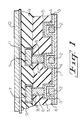
- Figure 1 is a cross-section of a device of the present invention.
- Figure 1 depicts a circuit subassembly (1) having device regions (2) and thin film metal wiring (3) interconnecting the devices.
- the metal wiring layers on conventional integrated circuit subassemblies are generally thin films of aluminum.
- these thin films can be made of high conductivity metals instead of aluminum.
- high conductivity metals are those having a resistivity below 2.5 microhm-centimeters at 20°C. These include copper, silver, gold, alloys and superconductors.
- PVD physical vapor deposition
- a silicon carbide layer is applied over the metallic wiring layer.
- this is accomplished by coating the entire top surface of the circuit subassembly which, obviously, includes the metal wiring. This is depicted as coating (4) in Figure 1.
- the silicon carbide may be selectively applied to the wiring alone by masking, for example, or the entire surface may be coated and then those areas where the silicon carbide is not desired etched away.
- Various methods of applying silicon carbide layers are known in the art. Examples of applicable methods include a variety of chemical vapor deposition techniques such as conventional CVD, photochemical vapor deposition, plasma enhanced chemical vapor deposition (PECVD), electron cyclotron resonance (ECR), jet vapor deposition and a variety of physical vapor deposition techniques such as sputtering or electron beam evaporation. These processes involve either the addition of energy (in the form of heat, plasma, etc.) to a vaporized species to cause the desired reaction, or the focusing of energy on a solid sample of the material to cause its deposition.
- chemical vapor deposition techniques such as conventional CVD, photochemical vapor deposition, plasma enhanced chemical vapor deposition (PECVD), electron cyclotron resonance (ECR), jet vapor deposition and a variety of physical vapor deposition techniques such as sputtering or electron beam evaporation.
- the coating is deposited by passing a stream of the desired precursor gases over a heated substrate. When the precursor gases contact the hot surface, they react and deposit the coating. Substrate temperatures in the range of 100-1000°C. are sufficient to form these coatings in several minutes to several hours, depending on the precursors and the thickness of the coating desired. If desired, reactive metals can be used in such a process to facilitate deposition.
- the desired precursor gases are reacted by passing them through a plasma field.
- the reactive species thereby formed are then focused at the substrate where they readily adhere.
- substrate temperatures can be used. For instance, substrate temperatures of 50°C. to 600°C. are functional.
- the plasma used in such processes comprises energy derived from a variety of sources such as electric discharges, electromagnetic fields in the radio-frequency or microwave range, lasers or particle beams.
- the use of radio frequency (10 kHz to 10 2 MHz) or microwave (0.1-10 GHz) energy, at moderate power densities (0.1-5 watts/cm 2 ) is generally preferred in most plasma deposition processes.
- the specific frequency, power and pressure are, however, generally tailored to the precursor gases and the equipment used.
- suitable precursor gases for use in these processes include (1) mixtures of one or more silanes and/or one or more halosilanes, e.g., trichlorosilane, with one or more alkanes of one to six carbon atoms, e.g., methane, ethane or propane; (2) an alkylsilane such as methylsilane, dimethylsilane or trimethylsilane; or (3) a silacyclobutane or disilacyclobutane as described in US-A-5,011,706.
- halosilanes e.g., trichlorosilane
- alkanes of one to six carbon atoms e.g., methane, ethane or propane
- an alkylsilane such as methylsilane, dimethylsilane or trimethylsilane
- silacyclobutane or disilacyclobutane as described in US-A-5,011,706.
- the plasma enhanced chemical vapor deposition of trimethylsilane is especially preferred for the purposes of this invention.
- a dielectric layer is then applied over the silicon carbide layer. This is shown as interlevel dielectric layer (5) in Figure 1.
- the specific dielectric layer and the method for its deposition are not critical to the invention. By using our process, however, one can utilize low dielectric constant (DK) layers. As used herein, low dielectric constant layers are those with a DK of less than 3.5.
- dielectric materials examples include silicon oxides, silicon nitrides, silicon oxynitrides, silicon carbides, silicon oxycarbides, silicon carbonitrides and organic materials such as silicones, polyimides, epoxy compounds or thermoplastic film polymers based on para-xylylene [PARYLENE TM - see also the definition of "parylene” in The Condensed Chemical Dictionary, Eighth Edition, Van Nostrand Reinhold Company, New York, p 660]. Obviously, more than one layer of these dielectrics may be used.
- the techniques for applying these coatings are also known in the art. They include spin-on processes, conventional CVD, photochemical vapor deposition, plasma enhanced chemical vapor deposition (PECVD), electron cyclotron resonance (ECR), jet vapor deposition and a variety of physical vapor deposition techniques such as sputtering and electron beam evaporation.
- various units of these resins may have either zero or more than one Si-H bond due to various factors involved in their formation and handling.
- Exemplary of these resins are those formed by the processes of US-A-3,615,272; US-A-5,010,159 US-A-4,999,397 and US-A-5,063,267. These resins are applied by a spin-on process followed by heating to convert them to a ceramic.
- Figure 1 shows such a second metal wiring layer (7) which is interconnected with selected regions of the first layer of wiring by interconnects (6).
- a layer of silicon carbide (8) should be deposited between the dielectric and the metal to prevent diffusion of the metal into the dielectric.
- This silicon carbide layer can be formed as described above. In such a manner, the metal wiring is sandwiched between layers of silicon carbide. This process can be repeated many times for the various layers of metallization within a circuit.
- Figure 1 shows a second layer of dielectric (9), and a third layer of wiring (10) protected by a third layer of silicon carbide (11).
- silicon carbide with a low dielectric constant may also replace the dielectric layer (i.e., layers 5 and 9 in Figure 1).
- a low dielectric constant e.g., DK ⁇ 5
- the dielectric layer i.e., layers 5 and 9 in Figure 1
Landscapes
- Internal Circuitry In Semiconductor Integrated Circuit Devices (AREA)
- Parts Printed On Printed Circuit Boards (AREA)
Priority Applications (1)
| Application Number | Priority Date | Filing Date | Title |
|---|---|---|---|
| DE29623946U DE29623946U1 (de) | 1995-02-02 | 1996-01-25 | Siliciumcarbidmetalldiffusionssperrschicht |
Applications Claiming Priority (2)
| Application Number | Priority Date | Filing Date | Title |
|---|---|---|---|
| US382701 | 1995-02-02 | ||
| US08/382,701 US5818071A (en) | 1995-02-02 | 1995-02-02 | Silicon carbide metal diffusion barrier layer |
Publications (3)
| Publication Number | Publication Date |
|---|---|
| EP0725440A2 true EP0725440A2 (de) | 1996-08-07 |
| EP0725440A3 EP0725440A3 (de) | 1997-01-29 |
| EP0725440B1 EP0725440B1 (de) | 2004-08-18 |
Family
ID=23510038
Family Applications (1)
| Application Number | Title | Priority Date | Filing Date |
|---|---|---|---|
| EP96300522A Expired - Lifetime EP0725440B1 (de) | 1995-02-02 | 1996-01-25 | Siliziumcarbid-Metall-Diffusionsbarriere-Schicht |
Country Status (6)
| Country | Link |
|---|---|
| US (1) | US5818071A (de) |
| EP (1) | EP0725440B1 (de) |
| JP (1) | JP3731932B2 (de) |
| KR (1) | KR100402187B1 (de) |
| DE (1) | DE69633150T2 (de) |
| TW (1) | TW284920B (de) |
Cited By (24)
| Publication number | Priority date | Publication date | Assignee | Title |
|---|---|---|---|---|
| WO1999030363A3 (en) * | 1997-12-10 | 1999-08-26 | Koninkl Philips Electronics Nv | Semiconductor device and method of manufacturing such a device |
| WO2000019498A1 (en) * | 1998-10-01 | 2000-04-06 | Applied Materials, Inc. | In situ deposition of low k si carbide barrier layer, etch stop, and anti-reflective coating for damascene applications |
| WO2000067304A1 (en) * | 1999-05-03 | 2000-11-09 | Interuniversitair Microelektronica Centrum (Imec) | Method for removal of sic |
| FR2794286A1 (fr) * | 1999-05-26 | 2000-12-01 | Commissariat Energie Atomique | Niveau d'interconnexion de type damascene pour dispositif micro-electronique |
| EP1096038A1 (de) | 1999-11-01 | 2001-05-02 | Applied Materials, Inc. | Verfahren und Vorrichtung zum Erzeugen einer Schicht |
| WO2001069672A1 (en) * | 2000-03-13 | 2001-09-20 | Koninklijke Philips Electronics N.V. | A method of manufacturing a semiconductor device |
| US6423384B1 (en) | 1999-06-25 | 2002-07-23 | Applied Materials, Inc. | HDP-CVD deposition of low dielectric constant amorphous carbon film |
| EP1263035A1 (de) * | 2001-05-23 | 2002-12-04 | Texas Instruments Incorporated | Verfahren zur Versiegelung der Kontaktlochseitenwände einer porösen Dielektrikumsschicht mit kleiner Dielektrizitätskonstante |
| US6559486B2 (en) * | 1999-12-01 | 2003-05-06 | Nec Electronics Corporation | Etching mask, process for forming contact holes using same, and semiconductor device made by the process |
| WO2003050870A1 (en) * | 2001-12-11 | 2003-06-19 | Trikon Technologies Limited | Diffusion barrier |
| US6635583B2 (en) | 1998-10-01 | 2003-10-21 | Applied Materials, Inc. | Silicon carbide deposition for use as a low-dielectric constant anti-reflective coating |
| US6656837B2 (en) | 2001-10-11 | 2003-12-02 | Applied Materials, Inc. | Method of eliminating photoresist poisoning in damascene applications |
| US6699784B2 (en) | 2001-12-14 | 2004-03-02 | Applied Materials Inc. | Method for depositing a low k dielectric film (K>3.5) for hard mask application |
| EP1094506A3 (de) * | 1999-10-18 | 2004-03-03 | Applied Materials, Inc. | Schutzschicht für Filme mit besonders kleiner Dielektrizitätskonstante |
| US6750141B2 (en) | 2001-03-28 | 2004-06-15 | Applied Materials Inc. | Silicon carbide cap layers for low dielectric constant silicon oxide layers |
| US6794311B2 (en) | 2000-07-14 | 2004-09-21 | Applied Materials Inc. | Method and apparatus for treating low k dielectric layers to reduce diffusion |
| US6838393B2 (en) | 2001-12-14 | 2005-01-04 | Applied Materials, Inc. | Method for producing semiconductor including forming a layer containing at least silicon carbide and forming a second layer containing at least silicon oxygen carbide |
| US6875687B1 (en) | 1999-10-18 | 2005-04-05 | Applied Materials, Inc. | Capping layer for extreme low dielectric constant films |
| US6926926B2 (en) | 2001-09-10 | 2005-08-09 | Applied Materials, Inc. | Silicon carbide deposited by high density plasma chemical-vapor deposition with bias |
| EP1233449A3 (de) * | 2001-02-15 | 2006-03-01 | Interuniversitair Micro-Elektronica Centrum | Verfahren zur Herstellung einer Halbleitervorrichtung |
| US7200460B2 (en) | 2001-02-23 | 2007-04-03 | Applied Materials, Inc. | Method of depositing low dielectric constant silicon carbide layers |
| EP1608013B1 (de) * | 2003-09-30 | 2013-04-24 | Imec | Herstellung von mit Luft gefüllten Lücken um eine Verbindungsleitung herum |
| US20130099329A1 (en) * | 2011-10-25 | 2013-04-25 | Stmicroelectronics (Crolles 2) Sas | Method for manufacturing insulated-gate mos transistors |
| US20210316331A1 (en) * | 2018-08-31 | 2021-10-14 | University Of Surrey | Apparatus and method for depositing a poly(p-xylylene) film on a component |
Families Citing this family (77)
| Publication number | Priority date | Publication date | Assignee | Title |
|---|---|---|---|---|
| KR100207444B1 (ko) * | 1995-03-14 | 1999-07-15 | 윤종용 | 반도체 장치의 고유전막/전극 및 그 제조방법 |
| US6350704B1 (en) | 1997-10-14 | 2002-02-26 | Micron Technology Inc. | Porous silicon oxycarbide integrated circuit insulator |
| US6627532B1 (en) * | 1998-02-11 | 2003-09-30 | Applied Materials, Inc. | Method of decreasing the K value in SiOC layer deposited by chemical vapor deposition |
| US6054379A (en) * | 1998-02-11 | 2000-04-25 | Applied Materials, Inc. | Method of depositing a low k dielectric with organo silane |
| JP4763131B2 (ja) * | 1998-10-01 | 2011-08-31 | アプライド マテリアルズ インコーポレイテッド | 低誘電率反射防止被膜に用いるシリコンカーバイドの堆積 |
| US6255217B1 (en) | 1999-01-04 | 2001-07-03 | International Business Machines Corporation | Plasma treatment to enhance inorganic dielectric adhesion to copper |
| US20050099078A1 (en) * | 1999-05-03 | 2005-05-12 | Serge Vanhaelemeersch | Method for removal of SiC |
| US6916399B1 (en) | 1999-06-03 | 2005-07-12 | Applied Materials Inc | Temperature controlled window with a fluid supply system |
| US6821571B2 (en) | 1999-06-18 | 2004-11-23 | Applied Materials Inc. | Plasma treatment to enhance adhesion and to minimize oxidation of carbon-containing layers |
| US6593653B2 (en) | 1999-09-30 | 2003-07-15 | Novellus Systems, Inc. | Low leakage current silicon carbonitride prepared using methane, ammonia and silane for copper diffusion barrier, etchstop and passivation applications |
| DE19951595A1 (de) * | 1999-10-27 | 2001-05-17 | Bosch Gmbh Robert | Massenflusssensor mit verbesserter Membranstabilität und einstellbarer Wärmeleitfähigkeit der Membran |
| US6541369B2 (en) * | 1999-12-07 | 2003-04-01 | Applied Materials, Inc. | Method and apparatus for reducing fixed charges in a semiconductor device |
| US6975030B1 (en) | 2000-01-10 | 2005-12-13 | Micron Technology, Inc. | Silicon carbide contact for semiconductor components |
| US6563215B1 (en) | 2000-01-10 | 2003-05-13 | Micron Technology, Inc. | Silicon carbide interconnect for semiconductor components and method of fabrication |
| US7033920B1 (en) | 2000-01-10 | 2006-04-25 | Micron Technology, Inc. | Method for fabricating a silicon carbide interconnect for semiconductor components |
| US6492267B1 (en) * | 2000-02-11 | 2002-12-10 | Micron Technology, Inc. | Low temperature nitride used as Cu barrier layer |
| US6417092B1 (en) * | 2000-04-05 | 2002-07-09 | Novellus Systems, Inc. | Low dielectric constant etch stop films |
| US6429129B1 (en) * | 2000-06-16 | 2002-08-06 | Chartered Semiconductor Manufacturing Ltd. | Method of using silicon rich carbide as a barrier material for fluorinated materials |
| US6764958B1 (en) * | 2000-07-28 | 2004-07-20 | Applied Materials Inc. | Method of depositing dielectric films |
| US6774489B2 (en) * | 2000-08-29 | 2004-08-10 | Texas Instruments Incorporated | Dielectric layer liner for an integrated circuit structure |
| US6936533B2 (en) * | 2000-12-08 | 2005-08-30 | Samsung Electronics, Co., Ltd. | Method of fabricating semiconductor devices having low dielectric interlayer insulation layer |
| JP3954312B2 (ja) * | 2001-01-15 | 2007-08-08 | ローム株式会社 | 半導体装置の製造方法 |
| US6469385B1 (en) * | 2001-06-04 | 2002-10-22 | Advanced Micro Devices, Inc. | Integrated circuit with dielectric diffusion barrier layer formed between interconnects and interlayer dielectric layers |
| KR100668819B1 (ko) * | 2001-06-26 | 2007-01-17 | 주식회사 하이닉스반도체 | 반도체 소자의 제조 방법 |
| US6541842B2 (en) * | 2001-07-02 | 2003-04-01 | Dow Corning Corporation | Metal barrier behavior by SiC:H deposition on porous materials |
| US6759327B2 (en) | 2001-10-09 | 2004-07-06 | Applied Materials Inc. | Method of depositing low k barrier layers |
| US6528423B1 (en) * | 2001-10-26 | 2003-03-04 | Lsi Logic Corporation | Process for forming composite of barrier layers of dielectric material to inhibit migration of copper from copper metal interconnect of integrated circuit structure into adjacent layer of low k dielectric material |
| US7091137B2 (en) | 2001-12-14 | 2006-08-15 | Applied Materials | Bi-layer approach for a hermetic low dielectric constant layer for barrier applications |
| US6890850B2 (en) | 2001-12-14 | 2005-05-10 | Applied Materials, Inc. | Method of depositing dielectric materials in damascene applications |
| US6849562B2 (en) * | 2002-03-04 | 2005-02-01 | Applied Materials, Inc. | Method of depositing a low k dielectric barrier film for copper damascene application |
| US6777349B2 (en) * | 2002-03-13 | 2004-08-17 | Novellus Systems, Inc. | Hermetic silicon carbide |
| US20030194496A1 (en) * | 2002-04-11 | 2003-10-16 | Applied Materials, Inc. | Methods for depositing dielectric material |
| US7008484B2 (en) * | 2002-05-06 | 2006-03-07 | Applied Materials Inc. | Method and apparatus for deposition of low dielectric constant materials |
| AU2003282533A1 (en) * | 2002-08-08 | 2004-02-25 | Trikon Technologies Limited | Improvements to showerheads |
| US7749563B2 (en) | 2002-10-07 | 2010-07-06 | Applied Materials, Inc. | Two-layer film for next generation damascene barrier application with good oxidation resistance |
| US7270713B2 (en) * | 2003-01-07 | 2007-09-18 | Applied Materials, Inc. | Tunable gas distribution plate assembly |
| US6790788B2 (en) * | 2003-01-13 | 2004-09-14 | Applied Materials Inc. | Method of improving stability in low k barrier layers |
| US6913992B2 (en) * | 2003-03-07 | 2005-07-05 | Applied Materials, Inc. | Method of modifying interlayer adhesion |
| US6942753B2 (en) | 2003-04-16 | 2005-09-13 | Applied Materials, Inc. | Gas distribution plate assembly for large area plasma enhanced chemical vapor deposition |
| US6972253B2 (en) * | 2003-09-09 | 2005-12-06 | Taiwan Semiconductor Manufacturing Company, Ltd. | Method for forming dielectric barrier layer in damascene structure |
| US6871537B1 (en) * | 2003-11-15 | 2005-03-29 | Honeywell International Inc. | Liquid flow sensor thermal interface methods and systems |
| US7030041B2 (en) | 2004-03-15 | 2006-04-18 | Applied Materials Inc. | Adhesion improvement for low k dielectrics |
| US7229911B2 (en) | 2004-04-19 | 2007-06-12 | Applied Materials, Inc. | Adhesion improvement for low k dielectrics to conductive materials |
| US7288205B2 (en) | 2004-07-09 | 2007-10-30 | Applied Materials, Inc. | Hermetic low dielectric constant layer for barrier applications |
| US20060021703A1 (en) * | 2004-07-29 | 2006-02-02 | Applied Materials, Inc. | Dual gas faceplate for a showerhead in a semiconductor wafer processing system |
| JP2006294671A (ja) * | 2005-04-06 | 2006-10-26 | Mitsui Chemicals Inc | 低誘電率炭化珪素膜の製造方法 |
| US20070210421A1 (en) * | 2006-03-13 | 2007-09-13 | Texas Instruments Inc. | Semiconductor device fabricated using a carbon-containing film as a contact etch stop layer |
| US7780865B2 (en) * | 2006-03-31 | 2010-08-24 | Applied Materials, Inc. | Method to improve the step coverage and pattern loading for dielectric films |
| US7601651B2 (en) * | 2006-03-31 | 2009-10-13 | Applied Materials, Inc. | Method to improve the step coverage and pattern loading for dielectric films |
| US20070287301A1 (en) * | 2006-03-31 | 2007-12-13 | Huiwen Xu | Method to minimize wet etch undercuts and provide pore sealing of extreme low k (k<2.5) dielectrics |
| US7604871B2 (en) * | 2006-06-07 | 2009-10-20 | Honeywell International Inc. | Electrical components including abrasive powder coatings for inhibiting tin whisker growth |
| US8247322B2 (en) | 2007-03-01 | 2012-08-21 | Taiwan Semiconductor Manufacturing Co., Ltd. | Via/contact and damascene structures and manufacturing methods thereof |
| US20090075470A1 (en) * | 2007-09-14 | 2009-03-19 | International Business Machines Corporation | Method for Manufacturing Interconnect Structures Incorporating Air-Gap Spacers |
| US20090072409A1 (en) | 2007-09-14 | 2009-03-19 | International Business Machines Corporation | Interconnect Structures Incorporating Air-Gap Spacers |
| JP2009088267A (ja) * | 2007-09-28 | 2009-04-23 | Tokyo Electron Ltd | 成膜方法、成膜装置、記憶媒体及び半導体装置 |
| JP2010103445A (ja) * | 2008-10-27 | 2010-05-06 | Toshiba Corp | 半導体装置及びその製造方法 |
| US20100320548A1 (en) * | 2009-06-18 | 2010-12-23 | Analog Devices, Inc. | Silicon-Rich Nitride Etch Stop Layer for Vapor HF Etching in MEMS Device Fabrication |
| US9340880B2 (en) | 2009-10-27 | 2016-05-17 | Silcotek Corp. | Semiconductor fabrication process |
| JP5735522B2 (ja) | 2009-10-27 | 2015-06-17 | シルコテック コーポレイション | 化学気相成長コーティング、物品、及び方法 |
| WO2012047945A2 (en) | 2010-10-05 | 2012-04-12 | Silcotek Corp. | Wear resistant coating, article, and method |
| US9975143B2 (en) | 2013-05-14 | 2018-05-22 | Silcotek Corp. | Chemical vapor deposition functionalization |
| US11292924B2 (en) | 2014-04-08 | 2022-04-05 | Silcotek Corp. | Thermal chemical vapor deposition coated article and process |
| US9915001B2 (en) | 2014-09-03 | 2018-03-13 | Silcotek Corp. | Chemical vapor deposition process and coated article |
| US10316408B2 (en) | 2014-12-12 | 2019-06-11 | Silcotek Corp. | Delivery device, manufacturing system and process of manufacturing |
| US10876206B2 (en) | 2015-09-01 | 2020-12-29 | Silcotek Corp. | Thermal chemical vapor deposition coating |
| US9653398B1 (en) * | 2015-12-08 | 2017-05-16 | Northrop Grumman Systems Corporation | Non-oxide based dielectrics for superconductor devices |
| US10323321B1 (en) | 2016-01-08 | 2019-06-18 | Silcotek Corp. | Thermal chemical vapor deposition process and coated article |
| US10608159B2 (en) | 2016-11-15 | 2020-03-31 | Northrop Grumman Systems Corporation | Method of making a superconductor device |
| US10487403B2 (en) | 2016-12-13 | 2019-11-26 | Silcotek Corp | Fluoro-containing thermal chemical vapor deposition process and article |
| US10276504B2 (en) | 2017-05-17 | 2019-04-30 | Northrop Grumman Systems Corporation | Preclean and deposition methodology for superconductor interconnects |
| US10763419B2 (en) | 2017-06-02 | 2020-09-01 | Northrop Grumman Systems Corporation | Deposition methodology for superconductor interconnects |
| US11161324B2 (en) | 2017-09-13 | 2021-11-02 | Silcotek Corp. | Corrosion-resistant coated article and thermal chemical vapor deposition coating process |
| US11195748B2 (en) | 2017-09-27 | 2021-12-07 | Invensas Corporation | Interconnect structures and methods for forming same |
| US10985059B2 (en) | 2018-11-01 | 2021-04-20 | Northrop Grumman Systems Corporation | Preclean and dielectric deposition methodology for superconductor interconnect fabrication |
| WO2020252306A1 (en) | 2019-06-14 | 2020-12-17 | Silcotek Corp. | Nano-wire growth |
| KR102815724B1 (ko) * | 2019-08-07 | 2025-06-04 | 삼성전자주식회사 | 반도체 장치 |
| US12473635B2 (en) | 2020-06-03 | 2025-11-18 | Silcotek Corp. | Dielectric article |
Family Cites Families (11)
| Publication number | Priority date | Publication date | Assignee | Title |
|---|---|---|---|---|
| DE2658304C2 (de) * | 1975-12-24 | 1984-12-20 | Tokyo Shibaura Electric Co., Ltd., Kawasaki, Kanagawa | Halbleitervorrichtung |
| JPS58204572A (ja) * | 1982-05-24 | 1983-11-29 | Semiconductor Energy Lab Co Ltd | 光電変換装置 |
| JPS59119733A (ja) * | 1982-12-24 | 1984-07-11 | Toshiba Corp | 半導体装置 |
| JPS59128281A (ja) * | 1982-12-29 | 1984-07-24 | 信越化学工業株式会社 | 炭化けい素被覆物の製造方法 |
| JPS63150963A (ja) * | 1986-12-12 | 1988-06-23 | Fujitsu Ltd | 半導体装置 |
| US5274268A (en) * | 1987-04-01 | 1993-12-28 | Semiconductor Energy Laboratory Co., Ltd. | Electric circuit having superconducting layered structure |
| US4960751A (en) * | 1987-04-01 | 1990-10-02 | Semiconductor Energy Laboratory Co., Ltd. | Electric circuit having superconducting multilayered structure and manufacturing method for same |
| JP2546696B2 (ja) * | 1987-12-17 | 1996-10-23 | 富士通株式会社 | シリコン炭化層構造 |
| KR930001428A (ko) * | 1991-06-12 | 1993-01-16 | 김광호 | 반도체장치의 제조방법 |
| JP2721603B2 (ja) * | 1991-09-25 | 1998-03-04 | 富士写真フイルム株式会社 | 固体撮像装置の駆動方法と固体撮像装置 |
| TW347149U (en) * | 1993-02-26 | 1998-12-01 | Dow Corning | Integrated circuits protected from the environment by ceramic and barrier metal layers |
-
1995
- 1995-02-02 US US08/382,701 patent/US5818071A/en not_active Expired - Lifetime
-
1996
- 1996-01-24 TW TW085100624A patent/TW284920B/zh not_active IP Right Cessation
- 1996-01-25 DE DE69633150T patent/DE69633150T2/de not_active Expired - Lifetime
- 1996-01-25 EP EP96300522A patent/EP0725440B1/de not_active Expired - Lifetime
- 1996-01-29 JP JP01242996A patent/JP3731932B2/ja not_active Expired - Lifetime
- 1996-02-02 KR KR1019960002496A patent/KR100402187B1/ko not_active Expired - Lifetime
Cited By (41)
| Publication number | Priority date | Publication date | Assignee | Title |
|---|---|---|---|---|
| US6201291B1 (en) | 1997-12-10 | 2001-03-13 | U.S. Philips Corporation | Semiconductor device and method of manufacturing such a device |
| WO1999030363A3 (en) * | 1997-12-10 | 1999-08-26 | Koninkl Philips Electronics Nv | Semiconductor device and method of manufacturing such a device |
| US6951826B2 (en) | 1998-10-01 | 2005-10-04 | Applied Materials, Inc. | Silicon carbide deposition for use as a low dielectric constant anti-reflective coating |
| KR100650226B1 (ko) * | 1998-10-01 | 2006-11-24 | 어플라이드 머티어리얼스, 인코포레이티드 | 낮은 κ 실리콘 카바이드 배리어층, 에칭 정지층, 및다마신 적용을 위한 반사방지 코팅층의 동일 현장 증착 |
| WO2000019498A1 (en) * | 1998-10-01 | 2000-04-06 | Applied Materials, Inc. | In situ deposition of low k si carbide barrier layer, etch stop, and anti-reflective coating for damascene applications |
| US6635583B2 (en) | 1998-10-01 | 2003-10-21 | Applied Materials, Inc. | Silicon carbide deposition for use as a low-dielectric constant anti-reflective coating |
| WO2000019508A1 (en) * | 1998-10-01 | 2000-04-06 | Applied Materials, Inc. | Silicon carbide deposition method and use as a barrier layer and passivation layer |
| KR100716622B1 (ko) * | 1998-10-01 | 2007-05-09 | 어플라이드 머티어리얼스, 인코포레이티드 | 유전상수가 낮은 반사 방지막으로 사용되는 규소 탄화물 및그 증착방법 |
| KR100696034B1 (ko) * | 1998-10-01 | 2007-03-16 | 어플라이드 머티어리얼스, 인코포레이티드 | 유전상수가 낮은 반사 방지막으로 사용되는 규소 탄화물및 그 증착방법 |
| WO2000020900A3 (en) * | 1998-10-01 | 2000-09-08 | Applied Materials Inc | Silicon carbide for use as a low dielectric constant anti-reflective coating and its deposition method |
| US6974766B1 (en) | 1998-10-01 | 2005-12-13 | Applied Materials, Inc. | In situ deposition of a low κ dielectric layer, barrier layer, etch stop, and anti-reflective coating for damascene application |
| US6599814B1 (en) | 1999-05-03 | 2003-07-29 | Interuniversitair Microelektronica Centrum (Imec) | Method for removal of sic |
| US6806501B2 (en) | 1999-05-03 | 2004-10-19 | Interuniverstair Microelektronica Centrum | Integrated circuit having SiC layer |
| WO2000067304A1 (en) * | 1999-05-03 | 2000-11-09 | Interuniversitair Microelektronica Centrum (Imec) | Method for removal of sic |
| FR2794286A1 (fr) * | 1999-05-26 | 2000-12-01 | Commissariat Energie Atomique | Niveau d'interconnexion de type damascene pour dispositif micro-electronique |
| US6423384B1 (en) | 1999-06-25 | 2002-07-23 | Applied Materials, Inc. | HDP-CVD deposition of low dielectric constant amorphous carbon film |
| EP1094506A3 (de) * | 1999-10-18 | 2004-03-03 | Applied Materials, Inc. | Schutzschicht für Filme mit besonders kleiner Dielektrizitätskonstante |
| US6875687B1 (en) | 1999-10-18 | 2005-04-05 | Applied Materials, Inc. | Capping layer for extreme low dielectric constant films |
| US6713390B2 (en) | 1999-11-01 | 2004-03-30 | Applied Materials Inc. | Barrier layer deposition using HDP-CVD |
| KR100743789B1 (ko) * | 1999-11-01 | 2007-07-30 | 어플라이드 머티어리얼스, 인코포레이티드 | Hdp-cvd를 이용하여 장벽층을 증착하기 위한 방법및 장치 |
| EP1096038A1 (de) | 1999-11-01 | 2001-05-02 | Applied Materials, Inc. | Verfahren und Vorrichtung zum Erzeugen einer Schicht |
| US6399489B1 (en) | 1999-11-01 | 2002-06-04 | Applied Materials, Inc. | Barrier layer deposition using HDP-CVD |
| US6617245B2 (en) | 1999-12-01 | 2003-09-09 | Nec Electronics Corporation | Etching mask, process for forming contact holes using same, and semiconductor device made by the process |
| US6559486B2 (en) * | 1999-12-01 | 2003-05-06 | Nec Electronics Corporation | Etching mask, process for forming contact holes using same, and semiconductor device made by the process |
| WO2001069672A1 (en) * | 2000-03-13 | 2001-09-20 | Koninklijke Philips Electronics N.V. | A method of manufacturing a semiconductor device |
| US6939812B2 (en) | 2000-03-13 | 2005-09-06 | Koninklijke Philips Electronics N.V. | Method of forming an etch stop layer in a semiconductor device |
| US6794311B2 (en) | 2000-07-14 | 2004-09-21 | Applied Materials Inc. | Method and apparatus for treating low k dielectric layers to reduce diffusion |
| EP1233449A3 (de) * | 2001-02-15 | 2006-03-01 | Interuniversitair Micro-Elektronica Centrum | Verfahren zur Herstellung einer Halbleitervorrichtung |
| US7200460B2 (en) | 2001-02-23 | 2007-04-03 | Applied Materials, Inc. | Method of depositing low dielectric constant silicon carbide layers |
| US6750141B2 (en) | 2001-03-28 | 2004-06-15 | Applied Materials Inc. | Silicon carbide cap layers for low dielectric constant silicon oxide layers |
| EP1263035A1 (de) * | 2001-05-23 | 2002-12-04 | Texas Instruments Incorporated | Verfahren zur Versiegelung der Kontaktlochseitenwände einer porösen Dielektrikumsschicht mit kleiner Dielektrizitätskonstante |
| US6926926B2 (en) | 2001-09-10 | 2005-08-09 | Applied Materials, Inc. | Silicon carbide deposited by high density plasma chemical-vapor deposition with bias |
| US7034409B2 (en) | 2001-10-11 | 2006-04-25 | Applied Materials Inc. | Method of eliminating photoresist poisoning in damascene applications |
| US6656837B2 (en) | 2001-10-11 | 2003-12-02 | Applied Materials, Inc. | Method of eliminating photoresist poisoning in damascene applications |
| WO2003050870A1 (en) * | 2001-12-11 | 2003-06-19 | Trikon Technologies Limited | Diffusion barrier |
| US6699784B2 (en) | 2001-12-14 | 2004-03-02 | Applied Materials Inc. | Method for depositing a low k dielectric film (K>3.5) for hard mask application |
| US6838393B2 (en) | 2001-12-14 | 2005-01-04 | Applied Materials, Inc. | Method for producing semiconductor including forming a layer containing at least silicon carbide and forming a second layer containing at least silicon oxygen carbide |
| EP1608013B1 (de) * | 2003-09-30 | 2013-04-24 | Imec | Herstellung von mit Luft gefüllten Lücken um eine Verbindungsleitung herum |
| US20130099329A1 (en) * | 2011-10-25 | 2013-04-25 | Stmicroelectronics (Crolles 2) Sas | Method for manufacturing insulated-gate mos transistors |
| US8878331B2 (en) * | 2011-10-25 | 2014-11-04 | Stmicroelectronics (Crolles 2) Sas | Method for manufacturing insulated-gate MOS transistors |
| US20210316331A1 (en) * | 2018-08-31 | 2021-10-14 | University Of Surrey | Apparatus and method for depositing a poly(p-xylylene) film on a component |
Also Published As
| Publication number | Publication date |
|---|---|
| TW284920B (de) | 1996-09-01 |
| DE69633150T2 (de) | 2005-08-18 |
| US5818071A (en) | 1998-10-06 |
| DE69633150D1 (de) | 2004-09-23 |
| JP3731932B2 (ja) | 2006-01-05 |
| JPH08250594A (ja) | 1996-09-27 |
| KR960032640A (ko) | 1996-09-17 |
| KR100402187B1 (ko) | 2004-02-11 |
| EP0725440B1 (de) | 2004-08-18 |
| EP0725440A3 (de) | 1997-01-29 |
Similar Documents
| Publication | Publication Date | Title |
|---|---|---|
| EP0725440B1 (de) | Siliziumcarbid-Metall-Diffusionsbarriere-Schicht | |
| US5563102A (en) | Method of sealing integrated circuits | |
| US5945155A (en) | Low dielectric constant amorphous fluorinated carbon and method of preparation | |
| US6268262B1 (en) | Method for forming air bridges | |
| EP0285445B1 (de) | Elektrische Schaltung mit supraleitender Mehrschichtstruktur und Herstellungsverfahren dafür | |
| EP0934127B1 (de) | Verfahren zur herstellung einer parylenbeschichtung | |
| JP4242648B2 (ja) | 金属イオン拡散バリア層 | |
| US20020106890A1 (en) | Method for multilevel copper interconnects for ultra large scale integration | |
| EP0434045B1 (de) | Verfahren zum selektiven Herstellen von leitendem Stoff | |
| CN1186814C (zh) | 扩散阻挡层和带扩散阻挡层的半导体器件及其制造方法 | |
| WO2000025361A1 (fr) | Dispositif a semi-conducteur et sa fabrication | |
| KR100624351B1 (ko) | 금속 필름의 화학적 증착 방법 | |
| McDonald et al. | Techniques for fabrication of wafer scale interconnections in multichip packages | |
| KR20010062216A (ko) | 반도체 장치에서 트래핑된 전하를 줄이기 위한 방법 및 장치 | |
| EP0661742B1 (de) | Verfahren zur Passivierung einer integrierten Schaltung | |
| US20020164889A1 (en) | Method for improving adhesion of low k materials with adjacent layer | |
| CN1302535C (zh) | 一种集成电路结构及其制造方法 | |
| EP0588577A2 (de) | Hermetisch abgedichtete integrierte Schaltungen | |
| DE29623946U1 (de) | Siliciumcarbidmetalldiffusionssperrschicht |
Legal Events
| Date | Code | Title | Description |
|---|---|---|---|
| PUAI | Public reference made under article 153(3) epc to a published international application that has entered the european phase |
Free format text: ORIGINAL CODE: 0009012 |
|
| AK | Designated contracting states |
Kind code of ref document: A2 Designated state(s): DE FR GB IT NL |
|
| PUAL | Search report despatched |
Free format text: ORIGINAL CODE: 0009013 |
|
| AK | Designated contracting states |
Kind code of ref document: A3 Designated state(s): DE FR GB IT NL |
|
| 17P | Request for examination filed |
Effective date: 19970221 |
|
| 17Q | First examination report despatched |
Effective date: 19971219 |
|
| APAB | Appeal dossier modified |
Free format text: ORIGINAL CODE: EPIDOS NOAPE |
|
| APAB | Appeal dossier modified |
Free format text: ORIGINAL CODE: EPIDOS NOAPE |
|
| APAD | Appeal reference recorded |
Free format text: ORIGINAL CODE: EPIDOS REFNE |
|
| APBT | Appeal procedure closed |
Free format text: ORIGINAL CODE: EPIDOSNNOA9E |
|
| GRAP | Despatch of communication of intention to grant a patent |
Free format text: ORIGINAL CODE: EPIDOSNIGR1 |
|
| GRAS | Grant fee paid |
Free format text: ORIGINAL CODE: EPIDOSNIGR3 |
|
| GRAA | (expected) grant |
Free format text: ORIGINAL CODE: 0009210 |
|
| AK | Designated contracting states |
Kind code of ref document: B1 Designated state(s): DE FR GB IT NL |
|
| REG | Reference to a national code |
Ref country code: GB Ref legal event code: FG4D |
|
| REF | Corresponds to: |
Ref document number: 69633150 Country of ref document: DE Date of ref document: 20040923 Kind code of ref document: P |
|
| PGFP | Annual fee paid to national office [announced via postgrant information from national office to epo] |
Ref country code: GB Payment date: 20050119 Year of fee payment: 10 |
|
| ET | Fr: translation filed | ||
| PLBE | No opposition filed within time limit |
Free format text: ORIGINAL CODE: 0009261 |
|
| STAA | Information on the status of an ep patent application or granted ep patent |
Free format text: STATUS: NO OPPOSITION FILED WITHIN TIME LIMIT |
|
| 26N | No opposition filed |
Effective date: 20050519 |
|
| APAH | Appeal reference modified |
Free format text: ORIGINAL CODE: EPIDOSCREFNO |
|
| PG25 | Lapsed in a contracting state [announced via postgrant information from national office to epo] |
Ref country code: GB Free format text: LAPSE BECAUSE OF NON-PAYMENT OF DUE FEES Effective date: 20060125 |
|
| GBPC | Gb: european patent ceased through non-payment of renewal fee |
Effective date: 20060125 |
|
| REG | Reference to a national code |
Ref country code: DE Ref legal event code: R082 Ref document number: 69633150 Country of ref document: DE Representative=s name: FLEISCHER, ENGELS & PARTNER MBB, PATENTANWAELT, DE |
|
| PGFP | Annual fee paid to national office [announced via postgrant information from national office to epo] |
Ref country code: NL Payment date: 20140110 Year of fee payment: 19 |
|
| PGFP | Annual fee paid to national office [announced via postgrant information from national office to epo] |
Ref country code: IT Payment date: 20140115 Year of fee payment: 19 Ref country code: FR Payment date: 20140108 Year of fee payment: 19 |
|
| PGFP | Annual fee paid to national office [announced via postgrant information from national office to epo] |
Ref country code: DE Payment date: 20150120 Year of fee payment: 20 |
|
| REG | Reference to a national code |
Ref country code: NL Ref legal event code: V1 Effective date: 20150801 |
|
| PG25 | Lapsed in a contracting state [announced via postgrant information from national office to epo] |
Ref country code: NL Free format text: LAPSE BECAUSE OF NON-PAYMENT OF DUE FEES Effective date: 20150801 |
|
| REG | Reference to a national code |
Ref country code: FR Ref legal event code: ST Effective date: 20150930 |
|
| PG25 | Lapsed in a contracting state [announced via postgrant information from national office to epo] |
Ref country code: FR Free format text: LAPSE BECAUSE OF NON-PAYMENT OF DUE FEES Effective date: 20150202 |
|
| PG25 | Lapsed in a contracting state [announced via postgrant information from national office to epo] |
Ref country code: IT Free format text: LAPSE BECAUSE OF NON-PAYMENT OF DUE FEES Effective date: 20150125 |
|
| REG | Reference to a national code |
Ref country code: DE Ref legal event code: R071 Ref document number: 69633150 Country of ref document: DE |