EP0717414B1 - Semiconductor memory - Google Patents
Semiconductor memory Download PDFInfo
- Publication number
- EP0717414B1 EP0717414B1 EP95116185A EP95116185A EP0717414B1 EP 0717414 B1 EP0717414 B1 EP 0717414B1 EP 95116185 A EP95116185 A EP 95116185A EP 95116185 A EP95116185 A EP 95116185A EP 0717414 B1 EP0717414 B1 EP 0717414B1
- Authority
- EP
- European Patent Office
- Prior art keywords
- sense amplifier
- signal line
- semiconductor memory
- bit lines
- circuit
- Prior art date
- Legal status (The legal status is an assumption and is not a legal conclusion. Google has not performed a legal analysis and makes no representation as to the accuracy of the status listed.)
- Expired - Lifetime
Links
- 239000004065 semiconductor Substances 0.000 title claims description 19
- 230000015654 memory Effects 0.000 claims description 30
- 229910052751 metal Inorganic materials 0.000 claims description 12
- 239000002184 metal Substances 0.000 claims description 12
- 238000009792 diffusion process Methods 0.000 claims description 11
- 239000012535 impurity Substances 0.000 claims description 11
- 229910021420 polycrystalline silicon Inorganic materials 0.000 claims description 11
- 229920005591 polysilicon Polymers 0.000 claims description 11
- 238000003491 array Methods 0.000 description 11
- 230000002093 peripheral effect Effects 0.000 description 8
- 239000011159 matrix material Substances 0.000 description 5
- 238000010586 diagram Methods 0.000 description 4
- 230000004913 activation Effects 0.000 description 1
- 229910052782 aluminium Inorganic materials 0.000 description 1
- XAGFODPZIPBFFR-UHFFFAOYSA-N aluminium Chemical compound [Al] XAGFODPZIPBFFR-UHFFFAOYSA-N 0.000 description 1
- 230000006399 behavior Effects 0.000 description 1
- 230000015572 biosynthetic process Effects 0.000 description 1
- 239000003990 capacitor Substances 0.000 description 1
- 238000001514 detection method Methods 0.000 description 1
- 230000004048 modification Effects 0.000 description 1
- 238000012986 modification Methods 0.000 description 1
- 238000009331 sowing Methods 0.000 description 1
- 239000000758 substrate Substances 0.000 description 1
- 230000007704 transition Effects 0.000 description 1
- WFKWXMTUELFFGS-UHFFFAOYSA-N tungsten Chemical compound [W] WFKWXMTUELFFGS-UHFFFAOYSA-N 0.000 description 1
- 229910052721 tungsten Inorganic materials 0.000 description 1
- 239000010937 tungsten Substances 0.000 description 1
Images


Classifications
-
- G—PHYSICS
- G11—INFORMATION STORAGE
- G11C—STATIC STORES
- G11C11/00—Digital stores characterised by the use of particular electric or magnetic storage elements; Storage elements therefor
- G11C11/21—Digital stores characterised by the use of particular electric or magnetic storage elements; Storage elements therefor using electric elements
- G11C11/34—Digital stores characterised by the use of particular electric or magnetic storage elements; Storage elements therefor using electric elements using semiconductor devices
- G11C11/40—Digital stores characterised by the use of particular electric or magnetic storage elements; Storage elements therefor using electric elements using semiconductor devices using transistors
- G11C11/401—Digital stores characterised by the use of particular electric or magnetic storage elements; Storage elements therefor using electric elements using semiconductor devices using transistors forming cells needing refreshing or charge regeneration, i.e. dynamic cells
- G11C11/4063—Auxiliary circuits, e.g. for addressing, decoding, driving, writing, sensing or timing
- G11C11/407—Auxiliary circuits, e.g. for addressing, decoding, driving, writing, sensing or timing for memory cells of the field-effect type
- G11C11/409—Read-write [R-W] circuits
- G11C11/4097—Bit-line organisation, e.g. bit-line layout, folded bit lines
-
- G—PHYSICS
- G11—INFORMATION STORAGE
- G11C—STATIC STORES
- G11C7/00—Arrangements for writing information into, or reading information out from, a digital store
- G11C7/18—Bit line organisation; Bit line lay-out
Definitions
- the present invention relates to a semiconductor memory, particularly to a dynamic-type semiconductor memory having a structure which reduces a pattern area by arranging sense amplifier arrays at both sides of a cell array in which dynamic-type memory cells are arranged in a matrix.
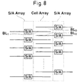
- FIG. 8 shows outline of a memory cell unit of a DRAM having the shared sense amplifier structure.
- Two sense amplifier arrays (S/A Array) are arranged at left and right ends of a memory cell array (Cell Array) having pairs of bit lines arranged in parallel with each other to interpose the memory cell array (Cell Array). Every other pair of bit lines are connected to sense amplifier circuits S/A in the left and right sense amplifier array (S/A Array).
- amplifier circuits of a number that is half of a number of the pairs of bit lines are arranged to the right sense amplifier array and sense amplifier circuits of the same number are arranged at the left sense amplifier array, respectively.
- the pairs of bit lines extend on the right side and on the left side of the sense amplifier circuits, respectively and are connected to pairs of bit lines of contiguous memory cell arrays, not shown. In operation either of the right side and the left side pair of bit lines is connected to the sense amplifier circuit by a select circuit, mentioned later.
- the two sense amplifier arrays (S/A Array) at the left and right ends of the memory cell array are operated to amplify memory cell data.
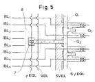
- Fig. 9 shows details of the senses amplifier circuit S/A approximately illustrated in Fig. 8.
- This sense amplifier circuit S/A can be divided into a left plane equalizing section, a left plane selecting section, a column gate section, a sense amplifier section, a right plane selecting section and a right plane equalizing section.
- the left plane equalizing section is constituted by N-channel MOS transistors Q1, Q2 and Q3 and equalizes left plane pair of bit lines BL1 and /BL1 to 1/2Vcc (Vcc is internal power source potential) supplied from VBL under control of a signal ⁇ EQL.
- the left plane selecting section is constituted by N-channel MOS transistor 14 and 15 and connects the column gate section and the sense amplifier section to the left plane pair of bit lines BL1 and /BL1 under control of signal ⁇ L.
- the column gate section is constituted by N-channel MOS transistors Q6 and Q7 and selectively connects the pair of bit lines to a pair of data lines DQ and /DQ under control of a column select line CSL.
- the sense amplifier section is constituted by N-channel MOS transistors Q8 through Q11 and P-channel MOS transistors Q12 and Q13 in which one of the pair of bit lines having a lower potential is drawn to "L" at a timing when a N-channel sense amplifier control line /SAN falls from 1/2 Vcc to 0V.
- a P-channel sense amplifier control line SAP rises from 1/2 Vcc to Vcc by which a P-channel sense amplifier is operated.
- a "H" side of the pair of bit lines is provided with a higher potential and detects a very small potential difference between the pair of bit lines.
- the right plane selecting section is constituted by N-channel MOS transistors Q14 and Q15 and connects the column gate section and the sense amplifier section to a right plane pair of bit lines BL1' and /BL1' under control of a signal ⁇ R.
- the right plane equalizing section is constituted by N-channel MOS transistors Q16, Q17 and Q18 and equalizes the right plane pair of bit lines BL1' and /BL1' to 1/2 Vcc supplied from VBL under control of a signal ⁇ R.
- EP-A-0 031 659 discloses a semiconductor memory device having a matrix area and a plurality of peripheral circuits.
- the memory cells are arranged at intersections of row and column wiring lines and the peripheral circuits such as sense amplifiers are connected to a predetermined number of adjacent wiring lines. Further, the peripheral circuits are arranged one after another (in ranks) when considered in a direction parallel to the lines. Especially, an arrangement of sense amplifiers at outer sides of the matrix arrangement is shown.
- US-A-5,272,665 discloses a semiconductor device having a matrix of memory cells.
- the memory cells are crossed by word lines and bit lines.
- word lines and bit lines In each group of adjacent bit lines there is a special arrangement of sense amplifiers.
- EP-A-0 496 406 discloses a semiconductor memory device having bit lines connected to memory cells and peripheral circuits such as sense amplifiers.
- the sense amplifiers are arranged at the sides of the matrix arrangement, which however consumes space between the bit lines at the respective other side of sense amplifiers.
- the means of the present invention it is possible to provide a constant space between the first and the second pairs of bit lines and the sense amplifier circuit opposing thereto and therefore, it is possible to provide a connection region for the signal lines. Further, it is similarly possible to provide a constant space between the third and the fourth pairs of bit lines and the sense amplifier circuit opposing thereto. Further, the mostly packed structure of the bit line arrangement is maintained as in the conventional shared sense amplifier structure. As a result, it is possible to achieve low resistance of equalize signal lines and the like without increasing chip area.
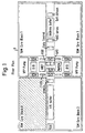
- Fig. 1 shows an outline structural view of a DRAM of the present invention.
- the total memory capacity is assumed to be that of a 64 M bits DRAM.
- Core blocks CB0, CB1, CB2 and CB3 each constituted by 16 M bits memory cells and peripheral circuits within a core section such as sense amplifiers, decoders and the like accompanying the memory cells, are arranged in a semiconductor chip 9.
- Vpp generating circuits Vpp Pump each generating a boosted voltage Vpp of a word line, are respectively arranged between CB0 and CB1, and CB2 and CB3.
- Data multiplexer circuits MUX and data buffer circuits DIB are respectively arranged at data output units of the respective core blocks CB.
- Fuse arrays CFUSE for holding replaced data of column redundancy circuits are arranged at the vicinities of the respective core blocks.
- a reference potential generating circuit VREF for generating a reference potential that is an intermediate potential of 1/2 VCC etc. is arranged between CB0 and CB1.
- a power-on reset circuit PWRON for generating an initializing signal when the internal portion of the chip is initialized in case where power source in on, is arranged between CB2 and CB3.
- a substrate potential generation circuit SSB, a data input/output buffer I/O buffer and Pad, a IO data multiplexer circuit X1MUX for selecting Pad in accordance with data output width are successively arranged between CB0 and CB2.
- a self refresh control circuit Self refresh, an address buffer Address buffer, a row series control circuit RAS series and a data control circuit DC are successively arranged between CB1 and CB3. Further, column partial decoder circuits CPD, an address transition detection circuit ATD, a row partial decoder circuit RPD and a column address switch circuit ASD are respectively arranged at the central portion of the chip 9.
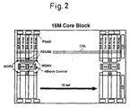
- Fig. 2 shows the structure of the 16 M bits core block CB.
- 32 sets of memory cell arrays (Cell Array) and 33 sets of sense amplifier arrays (peripheral circuits within a core section) (S/A Array) are alternately arranged constituting a memory cell block and column decoder circuits C/D are arranged at an end of the core block.
- a plurality of column select lines CSL are arranged in the row direction and are selectively driven by the column decoder circuits C/D.
- the column select lines CSL supply select signals to the sense amplifier array (S/A Array ) S/A at each row belonging to the same column. More in details the column select lines are used for partial activation of the sense amplifier circuits and for driving the column gate circuits.
- the memory cell block constitutes the 16 M bits core block CB by dividing it into top and bottom groups between which respectively arranged are row decoder circuits (for selectively driving word lines WL by internal row address signals) R/D each corresponding to each memory cell array, circuits WDRV for supplying drive signals to the row decoder circuits, circuits REUSE for holding replaced data of row redundancy circuits, data line amplifying circuit DQB, a block control circuit BC and the like.
- P-channel type sense amplifier drive circuits PSAD each corresponding to each peripheral circuit within a core section are respectively arranged at peripheral portions of the core block CB.
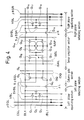
- Fig. 3 shows a structure of a memory cell arrays (Cell Array) interposed by two sense amplifier arrays (S/A Array).
- the memory cell array is of the shared sense amplifier structure in which two pairs of bit lines BL and /BL, and BL and /BL' are respectively connected to the respective sense amplifier circuits S/A and every two sense amplifiers are grouped and the groups are arranged in a staggered arrangement as shown in Fig. 3 thereby constituting a memory cell array.
- the locations of the sense amplifiers in view from the pairs of bit lines are on the right, right, left, left, right, right, left, left and so on, according to this embodiment although the locations are on the right, left, right, left, right, left, and so on according to the conventional example.
- constant spaces 8 are formed respectively among the two pairs of bit lines, for example, BL0 and /BL0, and Bl1 and /BL1, and the sense amplifier arrays (S/A Array).
- Each bit line is connected to a dynamic-type memory cell constituted by a transistor and a capacitor, not shown.
- Memory cells MC belonging to the same column are connected to the same pair of bit lines and those belonging to the same row are connected to the same word line.
- the word lines are selectively driven by the row decode circuits R/D as mentioned above.
- the row decode circuit includes at least a word line driving circuit charging the word lines at "H" level by P-channel type transistors, the drive signal supply circuits WDRV are used as their drive sources and the Vpp generating circuits Vpp Pump generating a boosted potential Vpp are used as their power sources.
- Fig. 4 shows details of the sense amplifier circuit S/A in Fig. 3. Many portions in this sense amplifier circuit are the same as those in the sense amplifier circuit explained in the conventional example.
- the sense amplifier circuit S/A can be divided into a left plane equalizing section, a left plane selecting section, a column gate section, a sense amplifier section, a right plane selecting section and a right plane equalizing section.
- the left plane equalizing section is constituted by the N-channel MOS transistors Q1, Q2 and Q3 and equalizes the left plane pair of bit lines BL1 and /BL1 to 1/2 Vcc supplied by SVBL under control of a signal S ⁇ EQL.
- the signal line S ⁇ EQL is made of a polysilicon wiring, is commonly used by the gate electrodes of the MOS transistors Q1, Q2 and Q3 and is provided with comparatively high resistance although the miniaturization thereof is possible.
- SVBL is composed of a wiring made of impurity diffusion, is commonly used for the drain electrodes of the MOS transistors Q1 and Q2 and also is provided with comparatively high resistance although the miniaturization thereof is possible.
- bypass lines ⁇ EQL and VBL composed of metal wiring layers are arranged in parallel with the wirings of S ⁇ EQL and SVBL and the both are brought into contact with each other at the regions of the spaces 8 (that is, shunted).
- the left plane selecting section is constituted by the N-channel MOS transistors Q4 and Q5 and connects the column gate section and the sense amplifier section to the left plane pair of bit lines BL1 and /BL1 under control of the signal ⁇ L.
- the column gate section is constituted by the N-channel MOS transistors Q6 and Q7 and selectively connects the pair of bit lines to the pair of data lines DQ and /DQ under control of the column select line CSL.
- the sense amplifier section is constituted by the N-channel MOS transistors Q8 through Q11 and the P-channel MOS transistors Q12 and Q13.
- the N-channel sense amplifier control line /SAN detects a "L" side line in the pair of bit lines toward the direction of 0 V at a timing when the N-channel sense amplifier control line /SAN falls from 1/2 Vcc to 0 V.
- the P-channel sense amplifier control line SAP detects a "H" side of the pair of bit lines toward the direction of Vcc at a timing when the P-channel sense amplifier control line SAP rises from 1/2 Vcc to Vcc.
- the amplifying operation is rapidly carried out by the MOS transistor Q10.
- the right plane selecting section is constituted by the N-channel MOS transistors Q14 and Q15 and connects the column gate section and the sense amplifier section to the right plane pair of bit lines BL1' and /BL1' under control of ⁇ R.
- the right plane equalizing section is constituted by the N-channel MOS transistors Q16, Q17 and Q18 and equalizes the right plane pair of bit lines BL1' and /BL1' to 1/2 Vcc supplied from SVBL under control of a signal S ⁇ EQR.
- the signal line S ⁇ EQR is made of a polysilicon wiring and commonly used by the gate electrodes of the MOS transistors Q16 and Q17 and Q18 as mentioned later and is provided with comparatively high resistance although the miniaturization thereof is possible.
- SVBL is composed of a wiring made of impurity diffusion as mentioned above, is commonly used by the drain electrodes of the MOS transistors Q17 and Q18 and also is provided with a comparatively high resistance although the miniaturization thereof is possible.
- bypass lines ⁇ EQR and VBL composed of metal wiring layers are arranged in parallel with the wirings of S ⁇ EQR and SVBL and the both are brought into contact with each other in the regions of the spaces 8, (that is, shunted).
- Fig. 5 shows a pattern diagram of the spaces 8 and its surrounding.
- S ⁇ EQL composed of a metal (aluminum or tungsten) wiring layer of low resistance having a width of 0.7 ⁇ m
- S ⁇ EQL composed of a polysilicon wiring layer of a comparatively high resistance having a width of 0.35 ⁇ m.
- S ⁇ EQL made of the polysilicon wiring layer is commonly used by the gate electrodes of the MOS transistors Q1, Q2 and Q3 and vertically traverses the memory cell array. Further, the hatched portion designates an impurity diffusion layer. It is not necessary to provide the contact region 7 at every space 8 and the space 8 may be provided at every other group of sense amplifiers. In this case, the vacant clearance 8 is used for shunting VBL, mentioned later.
- Fig. 6 shows a pattern diagram of the space 8, another member and its surrounding.
- a contact section 6 bringing the metal wiring and the impurity diffusion region in contact with each other and requiring also a comparatively large region, is formed in the space 8 that is a region contiguous to end portions of the pairs of bit lines BL6 and /BL6 and BL7 and /BL7 and which is surrounded by the two pairs of bit lines BL5 and /BL5 and BL8 and /BL8 and the equalizing circuits in the sense amplifier array (MOS transistors Q1, Q2 and Q3 etc.). (Naturally, it is possible to draw the electrode from the impurity diffusion region to the polysilicon layer once and connect the polysilicon layer to the metal wiring layer.
- VBL made of a metal wiring layer of low resistance having a width of 0.7 ⁇ m is connected to SVBL composed of a wiring made of impurity diffusion layer of comparatively high resistance having a width of 0.35 ⁇ m.
- SVBL composed of the impurity diffusion layer is commonly used by the drain electrodes of the MOS transistors Q1 and Q2 and vertically transverses the memory cell array. Further, the hatched portion designates the impurity diffusion layer.
- bit lines/sense amplifiers arrangement of the present invention since the constant spaces can be provided between the pairs of bit lines and the sense amplifiers.
- the mostly packed structure is maintained in the bit line arrangement (that is, 1 sense amplifier can be arranged at every 2 pairs of bit lines).
- low resistance formation of the equalizing signal lines etc. can be achieved without increasing chip area.
- Fig. 7(a) is a view approximately showing the bit lines/sense amplifiers arrangement of the above-mentioned embodiments.
- Fig. 7(b) shows a modified example thereof.
- the example is of a shared sense amplifier structure in which two pairs of bit lines are respectively connected to the left and the right of each sense amplifier circuit S/A as in the embodiments, every 4 sense amplifiers are grouped and arranged in a staggered arrangement thereby constituting a memory cell array different from the above-mentioned embodiments.
- the locations of the sense amplifiers in view from the pairs of bit lines are on the right, right, left, left, right, right, and so on in the conventional example.
- the locations are on the right, right, right, right, left, left, left, left, right, right, right, and so on.
- constant spaces are respectively formed between the 4 pairs of bit lines and the sense amplifier array.
- a large area is provided to the space in the modified example as compared with that in the above-mentioned examples.
- this arrangement is advantageous for the generation of 256 M bits DRAM etc. wherein miniaturization of polysilicon pitch is more advanced in providing contact (shunting) among signal lines.
- every 8 pairs of bit lines are grouped, by further advancing the embodiment in Fig. 7 (b).
Landscapes
- Engineering & Computer Science (AREA)
- Microelectronics & Electronic Packaging (AREA)
- Computer Hardware Design (AREA)
- Dram (AREA)
- Semiconductor Memories (AREA)
Applications Claiming Priority (3)
| Application Number | Priority Date | Filing Date | Title |
|---|---|---|---|
| JP6312990A JPH08172169A (ja) | 1994-12-16 | 1994-12-16 | 半導体記憶装置 |
| JP312990/94 | 1994-12-16 | ||
| JP31299094 | 1994-12-16 |
Publications (3)
| Publication Number | Publication Date |
|---|---|
| EP0717414A2 EP0717414A2 (en) | 1996-06-19 |
| EP0717414A3 EP0717414A3 (en) | 1996-11-06 |
| EP0717414B1 true EP0717414B1 (en) | 2001-03-14 |
Family
ID=18035914
Family Applications (1)
| Application Number | Title | Priority Date | Filing Date |
|---|---|---|---|
| EP95116185A Expired - Lifetime EP0717414B1 (en) | 1994-12-16 | 1995-10-13 | Semiconductor memory |
Country Status (7)
| Country | Link |
|---|---|
| US (1) | US5691933A (enExample) |
| EP (1) | EP0717414B1 (enExample) |
| JP (1) | JPH08172169A (enExample) |
| KR (1) | KR100254069B1 (enExample) |
| CN (1) | CN1093978C (enExample) |
| DE (1) | DE69520333T2 (enExample) |
| TW (1) | TW295662B (enExample) |
Families Citing this family (24)
| Publication number | Priority date | Publication date | Assignee | Title |
|---|---|---|---|---|
| JP3291206B2 (ja) * | 1996-09-17 | 2002-06-10 | 富士通株式会社 | 半導体記憶装置 |
| US5771268A (en) * | 1996-12-10 | 1998-06-23 | International Business Machines Corporation | High speed rotator with array method |
| US6067655A (en) * | 1997-08-28 | 2000-05-23 | Stmicroelectronics, N.V. | Burst error limiting symbol detector system |
| US6033945A (en) * | 1998-06-03 | 2000-03-07 | G-Link Technology | Multiple equilibration circuits for a single bit line |
| JP4339938B2 (ja) | 1998-06-10 | 2009-10-07 | 株式会社ルネサステクノロジ | 半導体記憶装置 |
| US7157314B2 (en) | 1998-11-16 | 2007-01-02 | Sandisk Corporation | Vertically stacked field programmable nonvolatile memory and method of fabrication |
| KR100319885B1 (ko) * | 1999-04-27 | 2002-01-10 | 윤종용 | 데이터 입출력 라인의 저항값을 줄이는 데이터 입출력 라인 구조 |
| US6188596B1 (en) * | 1999-05-20 | 2001-02-13 | Advanced Micro Devices, Inc. | Layout for semiconductor memory including multi-level sensing |
| US6163495A (en) | 1999-09-17 | 2000-12-19 | Cypress Semiconductor Corp. | Architecture, method(s) and circuitry for low power memories |
| TW503396B (en) * | 1999-12-03 | 2002-09-21 | Hitachi Ltd | Semiconductor device |
| US8575719B2 (en) | 2000-04-28 | 2013-11-05 | Sandisk 3D Llc | Silicon nitride antifuse for use in diode-antifuse memory arrays |
| US7184290B1 (en) * | 2000-06-28 | 2007-02-27 | Marvell International Ltd. | Logic process DRAM |
| KR100395877B1 (ko) * | 2000-11-10 | 2003-08-25 | 삼성전자주식회사 | 반도체 메모리의 데이타 감지 장치 |
| JP2003092364A (ja) * | 2001-05-21 | 2003-03-28 | Mitsubishi Electric Corp | 半導体記憶装置 |
| US6804145B2 (en) * | 2002-11-01 | 2004-10-12 | Hewlett-Packard Development Company, L.P. | Memory cell sensing system and method |
| WO2005117118A1 (ja) * | 2004-05-25 | 2005-12-08 | Renesas Technology Corp. | 半導体装置 |
| US7327591B2 (en) * | 2004-06-17 | 2008-02-05 | Texas Instruments Incorporated | Staggered memory cell array |
| US7218564B2 (en) * | 2004-07-16 | 2007-05-15 | Promos Technologies Inc. | Dual equalization devices for long data line pairs |
| JP4400497B2 (ja) * | 2005-03-31 | 2010-01-20 | エルピーダメモリ株式会社 | 半導体記憶装置 |
| JP4989900B2 (ja) * | 2006-01-31 | 2012-08-01 | ルネサスエレクトロニクス株式会社 | 並列演算処理装置 |
| JP4428384B2 (ja) | 2006-12-25 | 2010-03-10 | エルピーダメモリ株式会社 | 半導体記憶装置 |
| FR2972838B1 (fr) | 2011-03-18 | 2013-04-12 | Soitec Silicon On Insulator | Memoire a semi-conducteurs comportant des amplificateurs de lecture decales associes a un decodeur de colonne local |
| WO2014112472A1 (ja) * | 2013-01-15 | 2014-07-24 | ピーエスフォー ルクスコ エスエイアールエル | 半導体装置 |
| CN113129941A (zh) * | 2019-12-31 | 2021-07-16 | 福建省晋华集成电路有限公司 | 一种半导体存储器件 |
Family Cites Families (8)
| Publication number | Priority date | Publication date | Assignee | Title |
|---|---|---|---|---|
| JPS5683891A (en) * | 1979-12-13 | 1981-07-08 | Fujitsu Ltd | Semiconductor storage device |
| JPH07107797B2 (ja) * | 1987-02-10 | 1995-11-15 | 三菱電機株式会社 | ダイナミツクランダムアクセスメモリ |
| JPS6413290A (en) * | 1987-07-07 | 1989-01-18 | Oki Electric Ind Co Ltd | Semiconductor memory |
| US5280448A (en) * | 1987-11-18 | 1994-01-18 | Sony Corporation | Dynamic memory with group bit lines and associated bit line group selector |
| JP2691280B2 (ja) * | 1988-05-12 | 1997-12-17 | 三菱電機株式会社 | 半導体記憶装置 |
| DE69229067T2 (de) * | 1991-01-25 | 1999-12-09 | Nec Corp., Tokio/Tokyo | Halbleiterspeicheranordnung |
| KR100292170B1 (ko) * | 1991-06-25 | 2001-06-01 | 사와무라 시코 | 반도체기억장치 |
| JP2945216B2 (ja) * | 1992-09-17 | 1999-09-06 | シャープ株式会社 | 半導体メモリ装置 |
-
1994
- 1994-12-16 JP JP6312990A patent/JPH08172169A/ja active Pending
-
1995
- 1995-10-13 EP EP95116185A patent/EP0717414B1/en not_active Expired - Lifetime
- 1995-10-13 DE DE69520333T patent/DE69520333T2/de not_active Expired - Lifetime
- 1995-12-15 CN CN95120910A patent/CN1093978C/zh not_active Expired - Lifetime
- 1995-12-15 KR KR1019950050395A patent/KR100254069B1/ko not_active Expired - Fee Related
-
1996
- 1996-02-01 TW TW085101269A patent/TW295662B/zh not_active IP Right Cessation
- 1996-12-18 US US08/769,185 patent/US5691933A/en not_active Expired - Lifetime
Also Published As
| Publication number | Publication date |
|---|---|
| EP0717414A3 (en) | 1996-11-06 |
| KR960025729A (ko) | 1996-07-20 |
| EP0717414A2 (en) | 1996-06-19 |
| CN1134022A (zh) | 1996-10-23 |
| JPH08172169A (ja) | 1996-07-02 |
| CN1093978C (zh) | 2002-11-06 |
| TW295662B (enExample) | 1997-01-11 |
| DE69520333D1 (de) | 2001-04-19 |
| DE69520333T2 (de) | 2001-08-09 |
| KR100254069B1 (ko) | 2000-04-15 |
| US5691933A (en) | 1997-11-25 |
Similar Documents
| Publication | Publication Date | Title |
|---|---|---|
| EP0717414B1 (en) | Semiconductor memory | |
| US7177215B2 (en) | Semiconductor memory device operating at high speed and low power consumption | |
| US5815454A (en) | Semiconductor memory device having power line arranged in a meshed shape | |
| US6191990B1 (en) | Semiconductor integrated circuit device having stabilizing capacitors connected between power lines of main amplifiers | |
| US7161823B2 (en) | Semiconductor memory device and method of arranging signal and power lines thereof | |
| US6125070A (en) | Semiconductor memory device having multiple global I/O line pairs | |
| US6097648A (en) | Semiconductor memory device having plurality of equalizer control line drivers | |
| JP3028913B2 (ja) | 半導体記憶装置 | |
| JP3636233B2 (ja) | ワードドライバ回路及びそれを利用したメモリ回路 | |
| JP3267462B2 (ja) | 半導体記憶装置 | |
| US5384726A (en) | Semiconductor memory device having a capability for controlled activation of sense amplifiers | |
| US6838337B2 (en) | Sense amplifier and architecture for open digit arrays | |
| KR20230032455A (ko) | 펌핑 캐패시터 및 이를 포함하는 반도체 메모리 장치 | |
| US7324396B2 (en) | Sense amplifier organization for twin cell memory devices | |
| KR20040090178A (ko) | 반도체 메모리 장치 및 이 장치의 배치 방법 | |
| JPH11339494A (ja) | ダイナミック型ram | |
| JPH11354741A (ja) | ダイナミック型ram | |
| HK1017127A (en) | Space-efficient semiconductor memory having hierarchical column select line architecture |
Legal Events
| Date | Code | Title | Description |
|---|---|---|---|
| PUAI | Public reference made under article 153(3) epc to a published international application that has entered the european phase |
Free format text: ORIGINAL CODE: 0009012 |
|
| AK | Designated contracting states |
Kind code of ref document: A2 Designated state(s): DE FR GB |
|
| PUAL | Search report despatched |
Free format text: ORIGINAL CODE: 0009013 |
|
| AK | Designated contracting states |
Kind code of ref document: A3 Designated state(s): DE FR GB |
|
| 17P | Request for examination filed |
Effective date: 19970320 |
|
| 17Q | First examination report despatched |
Effective date: 19990730 |
|
| GRAG | Despatch of communication of intention to grant |
Free format text: ORIGINAL CODE: EPIDOS AGRA |
|
| GRAG | Despatch of communication of intention to grant |
Free format text: ORIGINAL CODE: EPIDOS AGRA |
|
| GRAH | Despatch of communication of intention to grant a patent |
Free format text: ORIGINAL CODE: EPIDOS IGRA |
|
| GRAH | Despatch of communication of intention to grant a patent |
Free format text: ORIGINAL CODE: EPIDOS IGRA |
|
| GRAA | (expected) grant |
Free format text: ORIGINAL CODE: 0009210 |
|
| AK | Designated contracting states |
Kind code of ref document: B1 Designated state(s): DE FR GB |
|
| REF | Corresponds to: |
Ref document number: 69520333 Country of ref document: DE Date of ref document: 20010419 |
|
| ET | Fr: translation filed | ||
| REG | Reference to a national code |
Ref country code: GB Ref legal event code: IF02 |
|
| PLBE | No opposition filed within time limit |
Free format text: ORIGINAL CODE: 0009261 |
|
| STAA | Information on the status of an ep patent application or granted ep patent |
Free format text: STATUS: NO OPPOSITION FILED WITHIN TIME LIMIT |
|
| 26N | No opposition filed | ||
| PGFP | Annual fee paid to national office [announced via postgrant information from national office to epo] |
Ref country code: GB Payment date: 20101013 Year of fee payment: 16 |
|
| PGFP | Annual fee paid to national office [announced via postgrant information from national office to epo] |
Ref country code: FR Payment date: 20111103 Year of fee payment: 17 |
|
| GBPC | Gb: european patent ceased through non-payment of renewal fee |
Effective date: 20121013 |
|
| REG | Reference to a national code |
Ref country code: FR Ref legal event code: ST Effective date: 20130628 |
|
| PG25 | Lapsed in a contracting state [announced via postgrant information from national office to epo] |
Ref country code: GB Free format text: LAPSE BECAUSE OF NON-PAYMENT OF DUE FEES Effective date: 20121013 |
|
| PG25 | Lapsed in a contracting state [announced via postgrant information from national office to epo] |
Ref country code: FR Free format text: LAPSE BECAUSE OF NON-PAYMENT OF DUE FEES Effective date: 20121031 |
|
| PGFP | Annual fee paid to national office [announced via postgrant information from national office to epo] |
Ref country code: DE Payment date: 20141007 Year of fee payment: 20 |
|
| REG | Reference to a national code |
Ref country code: DE Ref legal event code: R071 Ref document number: 69520333 Country of ref document: DE |