EP0716418A2 - Für Hochgeschwindigkeitsübertragung von Aufzeichnungsdaten geeignete Magnetkopftreiberschaltung und magneto-optisches Aufzeichnungsgerät damit - Google Patents
Für Hochgeschwindigkeitsübertragung von Aufzeichnungsdaten geeignete Magnetkopftreiberschaltung und magneto-optisches Aufzeichnungsgerät damit Download PDFInfo
- Publication number
- EP0716418A2 EP0716418A2 EP95119251A EP95119251A EP0716418A2 EP 0716418 A2 EP0716418 A2 EP 0716418A2 EP 95119251 A EP95119251 A EP 95119251A EP 95119251 A EP95119251 A EP 95119251A EP 0716418 A2 EP0716418 A2 EP 0716418A2
- Authority
- EP
- European Patent Office
- Prior art keywords
- power source
- signal
- magnetic head
- control pulse
- switching
- Prior art date
- Legal status (The legal status is an assumption and is not a legal conclusion. Google has not performed a legal analysis and makes no representation as to the accuracy of the status listed.)
- Granted
Links
Images


Classifications
-
- G—PHYSICS
- G11—INFORMATION STORAGE
- G11B—INFORMATION STORAGE BASED ON RELATIVE MOVEMENT BETWEEN RECORD CARRIER AND TRANSDUCER
- G11B5/00—Recording by magnetisation or demagnetisation of a record carrier; Reproducing by magnetic means; Record carriers therefor
- G11B5/02—Recording, reproducing, or erasing methods; Read, write or erase circuits therefor
-
- G—PHYSICS
- G11—INFORMATION STORAGE
- G11B—INFORMATION STORAGE BASED ON RELATIVE MOVEMENT BETWEEN RECORD CARRIER AND TRANSDUCER
- G11B11/00—Recording on or reproducing from the same record carrier wherein for these two operations the methods are covered by different main groups of groups G11B3/00 - G11B7/00 or by different subgroups of group G11B9/00; Record carriers therefor
- G11B11/10—Recording on or reproducing from the same record carrier wherein for these two operations the methods are covered by different main groups of groups G11B3/00 - G11B7/00 or by different subgroups of group G11B9/00; Record carriers therefor using recording by magnetic means or other means for magnetisation or demagnetisation of a record carrier, e.g. light induced spin magnetisation; Demagnetisation by thermal or stress means in the presence or not of an orienting magnetic field
- G11B11/105—Recording on or reproducing from the same record carrier wherein for these two operations the methods are covered by different main groups of groups G11B3/00 - G11B7/00 or by different subgroups of group G11B9/00; Record carriers therefor using recording by magnetic means or other means for magnetisation or demagnetisation of a record carrier, e.g. light induced spin magnetisation; Demagnetisation by thermal or stress means in the presence or not of an orienting magnetic field using a beam of light or a magnetic field for recording by change of magnetisation and a beam of light for reproducing, i.e. magneto-optical, e.g. light-induced thermomagnetic recording, spin magnetisation recording, Kerr or Faraday effect reproducing
- G11B11/10502—Recording on or reproducing from the same record carrier wherein for these two operations the methods are covered by different main groups of groups G11B3/00 - G11B7/00 or by different subgroups of group G11B9/00; Record carriers therefor using recording by magnetic means or other means for magnetisation or demagnetisation of a record carrier, e.g. light induced spin magnetisation; Demagnetisation by thermal or stress means in the presence or not of an orienting magnetic field using a beam of light or a magnetic field for recording by change of magnetisation and a beam of light for reproducing, i.e. magneto-optical, e.g. light-induced thermomagnetic recording, spin magnetisation recording, Kerr or Faraday effect reproducing characterised by the transducing operation to be executed
- G11B11/10504—Recording
- G11B11/10508—Recording by modulating only the magnetic field at the transducer
-
- G—PHYSICS
- G11—INFORMATION STORAGE
- G11B—INFORMATION STORAGE BASED ON RELATIVE MOVEMENT BETWEEN RECORD CARRIER AND TRANSDUCER
- G11B11/00—Recording on or reproducing from the same record carrier wherein for these two operations the methods are covered by different main groups of groups G11B3/00 - G11B7/00 or by different subgroups of group G11B9/00; Record carriers therefor
- G11B11/10—Recording on or reproducing from the same record carrier wherein for these two operations the methods are covered by different main groups of groups G11B3/00 - G11B7/00 or by different subgroups of group G11B9/00; Record carriers therefor using recording by magnetic means or other means for magnetisation or demagnetisation of a record carrier, e.g. light induced spin magnetisation; Demagnetisation by thermal or stress means in the presence or not of an orienting magnetic field
- G11B11/105—Recording on or reproducing from the same record carrier wherein for these two operations the methods are covered by different main groups of groups G11B3/00 - G11B7/00 or by different subgroups of group G11B9/00; Record carriers therefor using recording by magnetic means or other means for magnetisation or demagnetisation of a record carrier, e.g. light induced spin magnetisation; Demagnetisation by thermal or stress means in the presence or not of an orienting magnetic field using a beam of light or a magnetic field for recording by change of magnetisation and a beam of light for reproducing, i.e. magneto-optical, e.g. light-induced thermomagnetic recording, spin magnetisation recording, Kerr or Faraday effect reproducing
- G11B11/10595—Control of operating function
Definitions
- a recording head for a disk 91 is so constructed that an optical head 92 faces to a magnetic head 93 in such a manner as to put the disk 91 therebetween.
- the disk 91 has a vertically magnetized film 91a thereon.
- the optical head 92 includes an objective lens 94.
- a laser beam is irradiated from the optical head 92 upon the vertically magnetized film 91a to raise the temperature of a recording portion of the disk 91 to a temperature (approximately 180 °C) higher than the Curie temperature.
- a magnetic field of the N or S pole is applied from the magnetic head 93 to the vertically magnetized film 91a so that a magnetic pattern is recorded onto the vertically magnetized film 91a. Accordingly, recording of data onto the disk 91 is realized when the magnetic head 93 generates a magnetic field of the N or S polarity in accordance with data to be recorded.
- the magnetic head must give a sufficient magnetic field to a range of movement of a lens of the optical head in a tracking direction.
- the range of movement of the lens in the tracking direction is a region of the diameter of 0.6 to 1 mm.
- the magnetic head disposed in an opposing relationship to the optical head includes an E-shaped core.
- the E-shaped core has at a central portion thereof a rectangular parallelepiped center pole wound with a coil and at the opposite ends thereof a pair of rectangular parallelepiped side yokes which serve as side paths of a magnetic field.
- the coil has an inductance L of approximately 4 to 6 ⁇ H and a resistance value of 0.5 to 1 ⁇ .
- EFM data for driving a magnetic head undergo EFM modulation (Eight-Fourteen (8-14) modulation), and such EFM data are a pulse signal which exhibits a pulse reversal interval ranging from 3T at minimum to 11T at maximum.
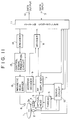
- FIG. 3 A circuit construction of a magnetic head driving system which can switchably use an ordinary transfer rate (for music applications) and a high transfer rate (for computer data or the like) is shown in FIG. 3.
- data such as audio data are supplied from a terminal 23 to an encoder 14.
- the data undergo CIRC (Cross Interleaved Reed Solomon Code) encoding, EFM modulation and some other necessary processing, to form an EFM signal.
- CIRC Cross Interleaved Reed Solomon Code
- the EFM signal is supplied to a control signal production circuit 15P.
- the control signal production circuit 15P includes a logic circuit 15Pa and produces and outputs control signals Sig1 to Sig6 for a magnetic head driving circuit 16 based on the EFM signal (Sig0).
- the magnetic head driving circuit 16 allows an electric current to flow into a coil 6L of a magnetic head 6 in response to the control signals Sig1 to Sig6 so that a magnetic field may be applied from the magnetic head 6 to a disk not shown in FIG. 3.
- a clock generation section 20 generates a clock signal for operation at an ordinary transfer rate.
- a clock frequency variation section 21 multiplies the frequency of the clock signal from the clock generation section 20 by the number of N, to produce another clock signal for operation at a high transfer rate.
- Either the clock signal for the ordinary rate from the clock generation section 20 or the clock signal for the high rate from the clock frequency variation section 21 is selected by a switching operation of a switch 22 in response to a switching signal Sel from a control section or a like element not shown.
- the selected clock signal is supplied as a processing clock signal CK to the encoder 14 and the control signal production circuit 15P.
- a recording operation is performed at the ordinary transfer rate, but when it is connected at an F terminal thereof, a recording operation is performed at the high transfer rate, for example, a rate equal to twice the ordinary transfer rate.
- the magnetic head driving circuit 16 is constructed as shown in FIG. 4.
- the magnetic head driving circuit 16 includes switching elements SW1 to SW6 to which the control signals Sig1 to Sig6 from the control signal production circuit 15P are inputted as switching control signals, respectively.
- a head terminal h1 connected to the coil 6L of the magnetic head 6 is connected to a positive dc power source 16a by way of the switching element SW1 and is grounded by way of the switching element SW5. Further, the head terminal h1 is connected to a negative dc power source 16b by way of the switching element SW3 and also by way of a diode D1.
- Another head terminal h2 connected to the other end of the coil 6L of the magnetic head 6 is connected to the positive dc power source 16a by way of the switching element SW2 and is grounded by way of the switching element SW6. Further, the head terminal h2 is connected to the negative dc power source 16b by way of the switching element SW4 and also by way of a diode D2.
- the potential +V of the positive dc power source 16a is set, for example, to +5 V
- the potential -V of the negative dc power source 16b is set, for example, approximately to -45 V.
- the ground is used as a power source of the 0 V potential.
- the logic circuit 15Pa of the control signal production circuit 15P which supplies the control signals Sig1 to Sig6 to the magnetic head driving circuit 16 is constructed as shown in FIG. 5 and produces the control signals Sig1 to Sig6 using the EFM signal (Sig0) and the clock signal CK.
- the EFM signal is supplied as the signal Sig0 to a terminal 50. Meanwhile, the clock signal CK is supplied to a terminal 57 by way of the switch 22 of FIG. 3.
- the logic circuit 15Pa includes invertors IV1 to IV7, flip-flops FF1 and FF2, AND gates A1 to A7, and delay circuits DL1 and DL2.
- the logic circuit 15Pa has output terminals 51 to 56 for outputting the control signals Sig1 to Sig6, respectively.
- the signal Sig0 is first supplied directly to the terminal 51. As seen from FIG. 6J, the signal Sig0 and the control signal Sig1 are the same signal.
- the signal Sig0 is logically inverted by the invertor IV1 and supplied as the control signal Sig2 to the terminal 52.
- the control signal Sig2 is such a control signal as seen from FIG. 6K.
- the invertor IV2, the flip-flop FF1 and the AND gate A1 function as a falling edge detection circuit, and the signal Sig0 is supplied to the invertor IV2 and the D terminal of the flip-flop FF1.
- the flip-flop FF1 performs a latching operation in response to the clock signal CK and outputs such a Q output as shown in FIG. 6C.
- the output of the invertor IV2 exhibits a waveform similar to that of the control signal Sig2 of FIG. 6K.
- the AND gate A1 performs AND-operation for the Q output of the flip-flop FF1 and the output of the invertor IV2, and the output thereof is shown in FIG. 6D.
- the AND output provides a falling edge detection pulse outputted in response to each falling edge of the signal Sig0.
- the falling edge detection pulse is supplied to the AND gate A4 and is also supplied to the AND gate A5 by way of the invertor IV6.
- the signal Sig0 is inverted by the invertor IV4 and supplied to the AND gate A5.
- the invertor IV3, the flip-flop FF2 and the AND gate A2 function as a rising edge detection circuit, and the signal Sig0 is supplied, after inverted by the invertor IV1, to the invertor IV3 and the D terminal of the flip-flop FF2.
- the flip-flop FF2 performs a latching operation in response to the clock signal CK and provides such a Q output as shown in FIG. 6E.
- the output of the invertor IV3 exhibits a waveform similar to that of the control signal Sig1 of FIG. 6J.
- the AND gate A2 performs AND-operation for the Q output of the flip-flop FF2 and the output of the invertor IV3 and provides a rising edge detection pulse which is outputted in response to each rising edge of the signal Sig0 as seen from FIG. 6F.
- the rising edge detection pulse is supplied to the AND gate A6 and is also supplied to the AND gate A7 by way of the invertor IV7.
- the signal Sig0 is inverted, after inverted by the invertor IV1, by the invertor IV5 again and supplied to the AND gate A7.
- the delay circuit DL1 delays the clock signal CK to produce a delayed clock signal CK D1 of FIG. 6G.
- the delay circuit DL2 delays the delayed clock signal CK D1 to produce another delayed clock signal CKD2 of FIG. 6H.
- the delayed clock signal CK D1 and the delayed clock signal CK D2 are supplied to the AND gate A3 so that a reference pulse signal illustrated in FIG. 6I is produced by the AND gate A3.
- the reference pulse signal is supplied to the AND gates A4, A5, A6 and A7.
- the AND gate A4 performs AND-operation for the falling edge detection pulse signal from the AND gate A1 and the reference pulse signal from the AND gate A3 to produce the control signal Sig3 as shown in FIG. 6L.
- the control signal Sig3 is outputted from the terminal 53.
- the AND gate A6 performs AND-operation for the rising edge detection pulse signal from the AND gate A2 and the reference pulse signal from the AND gate A3 to produce the control signal Sig4 as shown in FIG. 6M.
- the control signal Sig4 is outputted from the terminal 54.
- the AND gate A5 performs AND-operation for the output of the invertor IV4, the output of the invertor IV6 and the reference pulse signal and produces the control signal Sig5 as shown in FIG. 6N.
- the control signal Sig5 is outputted from the terminal 55.
- the AND gate A7 performs AND-operation for the output of the invertor IV5, the output of the invertor IV7 and the reference pulse signal to produce the control signal Sig6 as shown in FIG. 6O.
- the control signal Sig6 is outputted from the terminal 56.
- control signals Sig1 to Sig6 produced in such a manner as described above are supplied as control pulse signals to the switching elements SW1 to SW6 of the magnetic head driving circuit 16 of FIG. 4, respectively. Operation of the magnetic head driving circuit 16 based on the control signals Sig1 to Sig6 will be described below. It is to be noted that the description of the operation is given in connection with the points of time t1 and t2 between which the EFM signal exhibits the minimum reversal interval of 3T.
- the magnetic head driving circuit 16 of FIG. 4 upon reversal of the EFM signal can be represented as such an equivalent circuit as shown in FIG. 7.
- FIGs. 8A to 8E show timing charts of the control signals Sig1, Sig3 and Sig5, the head current Ih flowing through the coil 6L and the voltage Vh1 at the head terminal h1.
- the peak value of the head current Ih is approximately 0.5 A, and +V of the waveform diagram of the head terminal voltage Vh1 is approximately +5 V and -V is approximately -45 V.
- control signal Sig1 is reversed to the "L” level while the control signal Sig2 is reverted to the "H” signal. From this point of time, the waveforms vary as seen in FIGs. 8A to 8E. This will be described below with reference to an equivalent circuit shown in FIG. 7.
- the switching elements SW1, SW3 and SW5 are all off, and the head terminal h1 is disconnected from any voltage source. Meanwhile, since the switching element SW2 is on (not shown), the head terminal h2 is fixed to the +V voltage as can be seen from FIG. 7.
- the head terminal h1 side Since the head terminal h1 side is disconnected from all of the voltage sources, it sucks charge from a small floating capacitance. Accordingly, the voltage Vh1 of the head terminal h1 drops rapidly. As the voltage drop proceeds, the coil current Ih decreases little by little. Thus, an operation which can be seen from a t A period of FIG. 8D is performed.
- the voltage drop described above reaches the -V potential and is fixed there by the voltage source for -V by way of the diode D1.
- the switching element SW3 is turned on by the control signal Sig3 that is, within a t B period of FIG. 8E, charge moves from the -V power source (negative dc power source 16b) to the head terminal h1 side by way of the diode D1.
- the head terminal h1 is short-circuited to the -V power source (negative dc power source 16b). Consequently, the voltage Vh1 of the head terminal h1 is fixed to -V as seen within a t c period of FIG. 8E.
- control signal Sig5 is supplied at a required timing so that the head current Ih is kept substantially fixed as seen from FIG. 8D.
- an electric current flows in the direction of the head terminal h2 ⁇ h1 in response to the EFM signal of the "L" level, that is, in response to the control signal Sig1, and a magnetic field is generated from the magnetic head 6 in accordance with the direction of the electric current.
- an electric current flows in the direction of the head terminal h1 ⁇ h2 by similar operations by the control signals Sig1, Sig2, Sig4 and Sig6, and within this period of 4T, a magnetic field is generated from the magnetic head 6 in accordance with the direction of the electric current.
- the following values are substituted into the expression (4).
- V (-V) - (+V)
- V (-V) - (+V)
- L 5 x 10 ⁇ 6 (H)
- ⁇ i the electric current value of 0.5 A exhibited at an initial stage.
- FIGs. 9A to 9E Timing charts upon a recording operation at the high rate are shown in FIGs. 9A to 9E.
- the absolute time of, for example, the period of 3T is AT/2 in FIGs. 9A to 9E with respect to the time illustrated in FIGs. 8A to 8E.
- the control signals Sig1, Sig3 and Sig5 are pulse signals whose time base is 1/2 that in the case of FIGs. 8A to 8E (T ⁇ 115 nsec).
- the rise time t A is the same as that at the normal rate in the case of FIGs. 8A to 8E because it relies upon the coil 6L and the magnetic head driving circuit 16. Due to the fact that the rise time t A is the same, in the case of FIGs. 9A to 9E, the t B period, that is, the period after the voltage Vh1 reaches -V until the control signal Sig3 changes to the "H" level, is very short. In this instance, the time from a falling edge of the control signal Sig1 to a rising edge of the control signal Sig3 is approximately 58 nsec and is longer only a little than the rise time t A of approximately 50 nsec.
- FIGs. 10A to 10D Timing charts of the operation of the magnetic head driving circuit 16 at the three time rate are shown in FIGs. 10A to 10D.
- the absolute time of, for example, the period of 3T is reduced to AT/3, and as seen from FIGs. 10A to 10D, the control signals Sig1, Sig3 and Sig5 become pulse signals whose time base is reduced to 1/3 comparing with that in FIGs. 8A to 8E (T ⁇ 78 nsec).
- the rise time t A remains approximately 50 nsec and does not exhibit a variation from that at the normal rate shown in FIGs. 8A to 8E.
- the conventional magnetic head driving system of the construction described above cannot be applied when a high speed operation of three or more times a normal rate is intended.
- a recording apparatus comprising an optical head for irradiating a laser beam upon a face of a recording medium, a magnetic head disposed in an opposing relationship to a laser irradiation position at which the laser beam is irradiated for applying a magnetic field to the other face of the recording medium, an encoder for encoding a recording signal to be recorded onto the recording medium, power sources for providing at least a first power source voltage and a second power source voltage lower than the first power source voltage, a first switcher for switching connection to one end of a coil of the magnetic head at least between the first and second power source voltages, a second switcher for switching connection to the other end of the coil of the magnetic head at least between the first and second power source voltages, a control pulse generator for producing a control pulse for controlling the first and second switchers so that a total number of control pulses to be produced by the first and second switchers within a pulse reversal interval,
- a recording apparatus comprising an optical head for irradiating a laser beam upon a face of a recording medium, a magnetic head disposed in an opposing relationship to a laser irradiation position at which the laser beam is irradiated for applying a magnetic field to the other face of the recording medium, an encoder for encoding a recording signal to be recorded onto the recording medium, power sources for providing at least a first power source voltage and a second power source voltage lower than the first power source voltage, a first switcher for switching connection to one end of a coil of the magnetic head at least between the first and second power source voltages, a second switcher for switching connection to the other end of the coil of the magnetic head at least between the first and second power source voltages, control pulse generator for producing a control pulse for controlling the first switcher so that the second power source voltage may be connected to the one end of the coil of the magnetic head or another control signal for controlling the second switcher so that the second power source voltage may be connected to the
- a recording apparatus comprising an optical head for irradiating a laser beam upon a face of a recording medium, a magnetic head disposed in an opposing relationship to a laser irradiation position at which the laser beam is irradiated for applying a magnetic field to the other face of the recording medium, an encoder for encoding a recording signal to be recorded onto the recording medium, power sources for providing at least a first power source voltage and a second power source voltage lower than the first power source voltage, a first switcher for switching connection to one end of a coil of the magnetic head at least between the first and second power source voltages, second switcher for switching connection to the other end of the coil of the magnetic head at least between the first and second power source voltages, a first control pulse generator for producing a control pulse for controlling the first and second switchers so that a total number of control pulses to be produced by the first and second switchers within a pulse reversal interval, which is given by n x
- a magnetic head driving circuit comprising power sources for providing at least a first power source voltage and a second power source voltage lower than the first power source voltage, a first switcher for switching connection to one end of a coil of a magnetic head at least between the first and second power source voltages, a second switcher for switching connection to the other end of the coil of the magnetic head at least between the first and second power source voltages, a control pulse generator for producing a control pulse for controlling the first and second switchers so that a total number of control pulses to be produced by the first and second switchers within a pulse reversal interval, which is given by n x T, of a recording signal may be smaller than n, T being a transfer rate of the recording signal, n being a positive integral number, and a driver for driving the first and second switchers in response to the control pulse from the control pulse generator.
- control pulse generator includes a logic circuit having such production logic as just described as a second logic circuit in addition to a first logic circuit having a similar logical construction to that in the prior art, wherein either of the first and second logic circuits can be selectively used. Accordingly, a recording apparatus enabling high speed recording at a rate in a wide range from a normal rate to a high rate equal to or three times the normal rate can be realized.
- the optical head 3 includes a laser diode serving as laser beam outputting means, an optical system including a polarization beam splitter, an objective lens and so forth, and a detector for detecting reflected light.
- the objective lens 3a is held for displacement in a radial direction of the disk 1 and another direction toward and away from the disk 1 by a biaxial mechanism 4.
- the entire optical head 3 is mounted for movement in a radial direction of the disk 1 by a thread mechanism 5.
- a magnetic head 6 applies a magnetic field modulated in accordance with information supplied thereto to the magneto-optical disk 1.
- the magnetic head 6 is disposed in an opposing relationship to the optical head 3 across the disk 1.
- An address decoder 9 decodes the groove information to obtain absolute position information. Further, the address information recorded as data is extracted by the decoder section 8. The address information is supplied to the system controller 11, and is used for various controlling operations.
- information supplied, upon recording operation, from a terminal 13 to the system controller 11 as information to be recorded onto the disk 1 undergoes encoding processing such as CIRC encoding, EFM modulation and so forth by an encoder section 14 to produce an EFM signal.
- the EFM signal is supplied to a control signal production circuit 15.
- the control signal production circuit 15 produces control signals (Sig1 to Sig6) based on the EFM signal and supplies them to a magnetic head driving circuit 16.
- FIG. 12 is a block diagram of a magnetic head driving system in the first embodiment of the present invention which is incorporated in the recording and reproduction apparatus having the construction described above.
- One of the normal rate clock signal and the three time rate clock signal is selected by a switch 22 and supplied as a processing clock signal to the encoder 14 and the control signal production circuit 15. Changing over of the switch 22 is performed, for example, in response to a change-over control signal Sel from the system controller 11.
- the change-over control signal Sel is supplied also to the change-over circuit 15c to change over the same.
- the system controller 11 connects the switch 22 at the F terminal and the change-over circuit 15c at a B terminal using the change-over control signal Sel.
- the magnetic head driving circuit 16 may have a circuit construction, for example, similar to that described hereinabove with reference to FIG. 4.
- the switching elements SW1 to SW6 are controlled between on and off states in accordance with the control signals Sig1 to Sig6, respectively, and an electric current is supplied in a required direction to the coil 6L based on the operations of the switching elements SW1 to SW6.
- the normal rate logic circuit 15a in the control signal production circuit 15 has a similar construction to that of the logic circuit of FIG. 5.
- the switch 22 is connected at the F terminal so that the transfer rate is raised to three times. Further, the B terminal of the change-over circuit 15c is selected so that the control signals Sig1 to Sig6 from the high rate logic circuit 15b are supplied to the magnetic head driving circuit 16 having the construction of FIG. 4.
- the high rate logic circuit 15b is so constructed as shown in FIG. 13 and produces the control signals Sig1 to Sig6 using the EFM signal (Sig0) and the clock signal CK of the three time rate.
- the signal Sig0 is first supplied directly to the terminal 61 and makes such a control signal Sig1 as seen in FIG. 14J.
- the signal Sig0 is supplied to the D terminal of the flip-flop FF11 and the exclusive OR gate EX1.
- the flip-flop FF11 performs a latching operation in response to the clock signal CK and outputs such a Q output as shown in FIG. 14C.
- the Q output of the flip-flop FF11 is supplied to the exclusive OR gate EX1.
- the exclusive OR gate EX1 performs exclusive-OR operation for the Q output of the flip-flop FF11 of FIG. 14C and the signal Sig0 and provides such an output as shown in FIG. 14D.
- the output of the exclusive OR gate EX1 shown in FIG. 14D is supplied to the D terminal of the flip-flop FF12 and the NOR gate NR1.
- the flip-flop FF12 performs a latching operation in response to the clock signal CK and provides such a Q output as shown in FIG. 14E.
- the Q output of the flip-flop FF12 is supplied to the NOR gate NR1 and the AND gate A12.
- the NOR gate NR1 performs NOR-operation for the output of the exclusive OR gate EX1 shown in FIG. 14D and the Q output of the flip-flop FF12 shown in FIG. 14E and provides such an output as shown in FIG. 14F.
- the output of the NOR gate NR1 is supplied to the AND gate A11.
- the AND gate A11 performs AND-operation for the output of the NOR gate NR1 and the inverted clock signal CK-to produce such a logical AND output as shown in FIG. 14H.
- the AND gate A12 performs AND-operation for the Q output of the flip-flop FF12 and the inverted clock signal CK- to produce such a logical AND output as shown in FIG. 14I.
- the AND gate A15 performs AND-operation for the output of the AND gate A12 of FIG. 14I and the output of the invertor IV11 (which has the same waveform as the control signal Sig2) to produce such a control signal Sig3 as show in FIG. 14L.
- the control signal Sig3 is outputted from the terminal 63.
- the AND gate A16 performs AND-operation for the output of the AND gate A12 of FIG. 14I and the signal Sig0 to produce such a control signal Sig4 as shown in FIG. 14M.
- the control signal Sig4 is outputted from the terminal 64.
- the AND gate A13 performs AND-operation for the output of the AND gate A11 of FIG. 14H and the output of the invertor IV11 (which has the same waveform as the control signal Sig2) to produce such a control signal Sig5 as shown in FIG. 14N.
- the control signal Sig5 is outputted from the terminal 65.
- the AND gate A14 performs AND-operation for the output of the AND gate A11 and the signal Sig0 to produce such a control signal Sig6 as shown in FIG. 14O.
- the control signal Sig6 is outputted from the terminal 66.
- the control signals Sig1 to Sig6 produced by the high rate logic circuit 15b having the logical construction described above are supplied as control pulses to the magnetic head driving circuit 16, that is, to the switching elements SW1 to SW6 of the magnetic head driving circuit 16 of FIG. 4. Rising timings of the signal Sig3 to the switching element SW3 for short-circuiting the head terminal h1 to the -V power source within a "L" level period of the EFM signal and the control signal Sig4 to the switching element SW4 for short-circuiting the head terminal h2 to the -V power source within a "H" level period of the EFM signal are later than a timing after at least more than 1T elapses after a reversal timing of the EFM signal.
- the period from a point of time of a reversal to a rising edge of the control signal Sig3 or Sig4 can be set at least to a period longer than 78 nsec.
- the rising time is retarded comparing with the control signal Sig3 or Sig4 (illustrated in FIG. 6L or 6M) by the normal rate logic circuit 15a.
- the number of pulses which exhibit the high level within one reversal period is smaller than n where the reversal period is represented by nT.
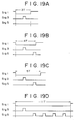
- FIGs. 15A, 15B, 15C and 15D show waveforms of the control signals Sig1, Sig3 and Sig5 within the "H" level period of the EFM signal when the "H" level period is 3T, 4T, 5T and 11T, respectively.
- the control signal Sig3 rises after an elapse of a timing of approximately 1.5T since a falling edge of the control signal Sig1.
- the total pulse number of the control signals Sig3 and Sig5 is 2 as can be seen from FIG. 15A and is smaller than "3" of 3T.
- FIGs. 16A to 16E These figures take as an example the points of time t1 and t2 between which the EFM signal exhibits a minimum reversal interval of 3T.
- FIGs. 16D and 16E show timing charts of the head current Ih flowing through the coil 6L and the voltage Vh1 at the head terminal h1. It is assumed that the peak value of the head current Ih is 0.5 A, and +V in the waveform diagram of the voltage Vh1 is approximately +5 V and -V is approximately -45 V.
- a recording operation at a three time rate which has conventionally been impossible, can be performed without any modification to the construction of the magnetic head driving circuit 16 or the magnetic head 6.
- a recording operation at a rate higher than the three time rate can be of course realized.
- the high rate logic circuit 15b is different from that in the first embodiment.
- the high rate logic circuit 15b has a construction shown in FIG. 17 for producing control signals Sig1 to Sig6 using an EFM signal (Sig0) and a clock signal CK of the three time rate.
- the high rate logic circuit 15b is different in construction from that of FIG. 12 in that it additionally includes a flip-flop FF13 and an invertor IV13, which are surrounded by a broken line in FIG. 17, and the output of the NOR gate NR1 is used as a clear signal for the flip-flop FF13 and that the Q output of the flip-flop FF13 is supplied to the AND gate A11.
- a clock signal CK is supplied to the flip-flop FF13.
- the Q output of the flip-flop FF13 is inverted by the invertor IV13 and supplied to the D terminal of the flip-flop FF13. Since the output of the NOR gate NR1 shown in FIG. 18F is used as a clear signal for the flip-flop FF13, the Q output of the flip-flop FF13 exhibits such a waveform as shown in FIG. 18G.
- the Q output of the flip-flop FF13 is supplied to the AND gate A11.
- the AND gate A11 performs AND-operation for the Q output of the flip-flop FF13 and an inverted clock signal of FIG. 18H, which is the output of the invertor IV12, to provide such an output as shown in FIG. 18I.
- the output of the AND gate A11 is supplied to the AND gates A13 and A14 and used for production of control signals Sig5 and Sig6, respectively.
- the AND gate A13 performs AND-operation for the output of the AND gate A11 and the output of the invertor IV11 (which has the same waveform as the control signal Sig2) to produce such a control signal Sig5 as shown in FIG. 18O.
- the AND gate A14 performs AND-operation for the output of the AND gate A11 and the signal Sig0 to produce such a control signal Sig6 as shown in FIG. 18P.
- the other control signals Sig1 to Sig4 are such as shown in FIGs. 18K to 18N and are similar to the control signals Sig1 to Sig4 of FIGs. 14J to 14M, respectively.
- FIGs. 19A to 19D the waveforms of the control signals Sig1, Sig3 and Sig5 within a "H" level period of the EFM signal are shown in FIGs. 19A to 19D when the "H" level period is 3T, 4T, 5T and 11T, respectively.
- the control signal Sig3 rises after an elapse of a time of approximately 1.5T since a falling edge of the control signal Sig1. Further, when the "H" level period is 3T, the total pulse number of the control signals Sig3 and Sig5 is 1 as seen from FIG. 19A and is smaller than "3" of 3T. Similarly, when the "H" level period is 11T, the total pulse number of the control signals Sig3 and Sig5 is 5 as seen from FIG. 19D and is smaller than "11" of 11T.
- the switching element SW3 is not turned on in response to the control signal Sig3 until the voltage of the head terminal h1 drops to the -V potential and is then fixed to the voltage source of -V by the diode D1. Then, the switching element SW3 is turned on in response to the control signal Sig3 only after an elapse of an interval of time indicated by tz in FIG. 16B since a falling edge of the control signal Sig1.
- the switching element SW3 is turned on, the head terminal h1 is short-circuited to the -V power source (negative dc power source 16b) so that the voltage Vh1 is thereafter fixed to -V.
- t z approximately 117 ns
- the voltage Vh1 of the head terminal h1 is substantially equal to the -V potential.
- the switching element SW3 can be turned on. Accordingly, an appropriate operation by a high speed switching element can be realized.
- a recording operation at a three time rate which has conventionally been impossible, can be performed without any modification to the construction of the magnetic head driving circuit 16 or the magnetic head 6.
- a recording operation at a rate higher than the three time rate can be of course realized.
- control signal production circuit 15 does not include a normal rate logic circuit but includes only the high rate logic circuit 15b.
- the high rate logic circuit 15b may be so constructed as shown in FIG. 13 or 17.
- the present embodiment is constructed as a recording apparatus for exclusive use for a high rate.
- the frequency of the clock signal CK is made variable so that the recording apparatus may operate at a plurality of different transfer rates.
Applications Claiming Priority (3)
| Application Number | Priority Date | Filing Date | Title |
|---|---|---|---|
| JP33038594 | 1994-12-07 | ||
| JP330385/94 | 1994-12-07 | ||
| JP33038594A JP3351148B2 (ja) | 1994-12-07 | 1994-12-07 | 記録装置、磁気ヘッド駆動装置 |
Publications (3)
| Publication Number | Publication Date |
|---|---|
| EP0716418A2 true EP0716418A2 (de) | 1996-06-12 |
| EP0716418A3 EP0716418A3 (de) | 1997-02-26 |
| EP0716418B1 EP0716418B1 (de) | 2002-08-28 |
Family
ID=18232014
Family Applications (1)
| Application Number | Title | Priority Date | Filing Date |
|---|---|---|---|
| EP95119251A Expired - Lifetime EP0716418B1 (de) | 1994-12-07 | 1995-12-06 | Für Hochgeschwindigkeitsübertragung von Aufzeichnungsdaten geeignete Magnetkopftreiberschaltung und magneto-optisches Aufzeichnungsgerät damit |
Country Status (6)
| Country | Link |
|---|---|
| US (2) | US5654943A (de) |
| EP (1) | EP0716418B1 (de) |
| JP (1) | JP3351148B2 (de) |
| KR (1) | KR100378836B1 (de) |
| CN (1) | CN1075224C (de) |
| DE (1) | DE69527921T2 (de) |
Cited By (1)
| Publication number | Priority date | Publication date | Assignee | Title |
|---|---|---|---|---|
| EP1069557A3 (de) * | 1999-07-12 | 2002-09-11 | Fujitsu Limited | Treiberschaltung für magnetische Köpfe und Wicklungsanordnungen von magnetischen Köpfen |
Families Citing this family (6)
| Publication number | Priority date | Publication date | Assignee | Title |
|---|---|---|---|---|
| US5898532A (en) * | 1996-07-02 | 1999-04-27 | Seagate Technology Inc. | MR head thermal asperity recovery |
| JP3573997B2 (ja) * | 1999-03-31 | 2004-10-06 | 三洋電機株式会社 | 磁気ヘッド駆動回路および磁気記録装置 |
| SG96239A1 (en) | 2000-09-27 | 2003-05-23 | Seagate Technology Llc | Data head writer coil testing |
| JP4105407B2 (ja) * | 2001-06-15 | 2008-06-25 | 富士通株式会社 | 磁界印加装置用コイル駆動回路及び情報記憶装置並びに磁界印加装置用コイル駆動制御方法 |
| AU2002323295A1 (en) | 2002-03-29 | 2003-10-20 | Seagate Technology Llc | Mr head thermal asperity cancellation |
| WO2008126194A1 (ja) * | 2007-03-19 | 2008-10-23 | Fujitsu Limited | 磁気記録回路、磁気記録装置、および情報記録方法 |
Family Cites Families (10)
| Publication number | Priority date | Publication date | Assignee | Title |
|---|---|---|---|---|
| JPH0833974B2 (ja) * | 1987-08-19 | 1996-03-29 | ソニー株式会社 | 磁気ヘッド駆動回路 |
| US5121369A (en) * | 1989-05-25 | 1992-06-09 | International Business Machines Corporation | Method and apparatus for direct overwriting information on a magneto-optical recording medium using constant laser beam modulated magnetic field generator |
| JP3097088B2 (ja) * | 1989-12-27 | 2000-10-10 | ソニー株式会社 | 磁気ヘッド駆動回路 |
| US5278809A (en) * | 1990-01-17 | 1994-01-11 | Olympus Optical Co., Ltd. | Photomagnetic recording apparatus recording with alternating magnetic field and D.C. magnetic field |
| JP3141242B2 (ja) * | 1990-08-24 | 2001-03-05 | ソニー株式会社 | 光ディスク記録装置 |
| JP3065404B2 (ja) * | 1991-11-18 | 2000-07-17 | シャープ株式会社 | 外部磁界発生装置 |
| JPH05151758A (ja) * | 1991-11-28 | 1993-06-18 | Sharp Corp | 情報記録再生装置 |
| JP3188339B2 (ja) * | 1992-03-06 | 2001-07-16 | キヤノン株式会社 | 磁気ヘッド駆動装置および光磁気記録装置 |
| EP0565751A1 (de) * | 1992-04-14 | 1993-10-20 | Pioneer Electronic Corporation | Optisches Aufzeichnungsverfahren und Gerät dafür |
| JP3179276B2 (ja) * | 1993-03-26 | 2001-06-25 | キヤノン株式会社 | 磁気ヘッド駆動方法および光磁気記録方法 |
-
1994
- 1994-12-07 JP JP33038594A patent/JP3351148B2/ja not_active Expired - Fee Related
-
1995
- 1995-11-30 US US08/565,008 patent/US5654943A/en not_active Expired - Lifetime
- 1995-12-06 EP EP95119251A patent/EP0716418B1/de not_active Expired - Lifetime
- 1995-12-06 KR KR1019950047043A patent/KR100378836B1/ko not_active Expired - Fee Related
- 1995-12-06 DE DE69527921T patent/DE69527921T2/de not_active Expired - Fee Related
- 1995-12-07 CN CN95121756A patent/CN1075224C/zh not_active Expired - Fee Related
-
1996
- 1996-10-08 US US08/727,054 patent/US5748573A/en not_active Expired - Fee Related
Non-Patent Citations (1)
| Title |
|---|
| None |
Cited By (2)
| Publication number | Priority date | Publication date | Assignee | Title |
|---|---|---|---|---|
| EP1069557A3 (de) * | 1999-07-12 | 2002-09-11 | Fujitsu Limited | Treiberschaltung für magnetische Köpfe und Wicklungsanordnungen von magnetischen Köpfen |
| US6570725B1 (en) | 1999-07-12 | 2003-05-27 | Fujitsu Limited | Drive circuit for magnetic head and winding configuration of magnetic head suitable for the drive circuit |
Also Published As
| Publication number | Publication date |
|---|---|
| CN1075224C (zh) | 2001-11-21 |
| CN1135076A (zh) | 1996-11-06 |
| KR960025328A (ko) | 1996-07-20 |
| EP0716418B1 (de) | 2002-08-28 |
| EP0716418A3 (de) | 1997-02-26 |
| JPH08167191A (ja) | 1996-06-25 |
| US5654943A (en) | 1997-08-05 |
| DE69527921D1 (de) | 2002-10-02 |
| US5748573A (en) | 1998-05-05 |
| DE69527921T2 (de) | 2003-05-08 |
| KR100378836B1 (ko) | 2003-08-30 |
| JP3351148B2 (ja) | 2002-11-25 |
Similar Documents
| Publication | Publication Date | Title |
|---|---|---|
| US4740939A (en) | Apparatus for reproducing information recorded on a disk | |
| EP0716418A2 (de) | Für Hochgeschwindigkeitsübertragung von Aufzeichnungsdaten geeignete Magnetkopftreiberschaltung und magneto-optisches Aufzeichnungsgerät damit | |
| US5991242A (en) | Magnetic head drive device, and magneto-optical recording apparatus using the same | |
| US6084830A (en) | Signal reproducing apparatus for reproducing information by moving magnetic walls | |
| US20010028607A1 (en) | Reproduction power test method for domain-wall displacement type magneto-optical medium and optical information reproduction apparatus | |
| US8030994B2 (en) | Driver for an inductive load | |
| JP3406133B2 (ja) | 光学記憶装置 | |
| JP4216555B2 (ja) | ブレーキ信号発生回路及び発生方法 | |
| EP0557094A1 (de) | Magnetkopg-Antriebsvorrichtung | |
| JP2880743B2 (ja) | 光磁気記録用外部印加磁界供給装置 | |
| US20030206502A1 (en) | Method and apparatus for providing motor control in an optical disk drive system | |
| JP2501915B2 (ja) | 光記録再生装置 | |
| JPH11162036A (ja) | 記録装置 | |
| JPH02287924A (ja) | オフトラック検出装置 | |
| US6477119B2 (en) | Magnetic head drive circuit including paired auxiliary coils, paired switching elements, and switch element control circuit, and magneto-optical recording device using the same | |
| JP3024662B2 (ja) | コイル駆動装置および情報記録装置 | |
| JP3140564B2 (ja) | 磁気ヘッド装置 | |
| JPH02232827A (ja) | 光記録媒体用レーザ駆動回路 | |
| JPH06274803A (ja) | 磁気記録装置 | |
| JP2003085845A (ja) | 光磁気記録再生装置 | |
| JPH03272038A (ja) | 磁気ヘッド装置 | |
| JPH1196609A (ja) | 光磁気情報再生装置 | |
| JP2005078773A (ja) | 磁気ヘッド駆動回路 | |
| JPH0563844B2 (de) | ||
| JPH04289544A (ja) | 光磁気記録再生装置 |
Legal Events
| Date | Code | Title | Description |
|---|---|---|---|
| PUAI | Public reference made under article 153(3) epc to a published international application that has entered the european phase |
Free format text: ORIGINAL CODE: 0009012 |
|
| AK | Designated contracting states |
Kind code of ref document: A2 Designated state(s): DE FR GB |
|
| PUAL | Search report despatched |
Free format text: ORIGINAL CODE: 0009013 |
|
| AK | Designated contracting states |
Kind code of ref document: A3 Designated state(s): DE FR GB |
|
| 17P | Request for examination filed |
Effective date: 19970728 |
|
| 17Q | First examination report despatched |
Effective date: 19991105 |
|
| GRAG | Despatch of communication of intention to grant |
Free format text: ORIGINAL CODE: EPIDOS AGRA |
|
| GRAG | Despatch of communication of intention to grant |
Free format text: ORIGINAL CODE: EPIDOS AGRA |
|
| GRAH | Despatch of communication of intention to grant a patent |
Free format text: ORIGINAL CODE: EPIDOS IGRA |
|
| GRAH | Despatch of communication of intention to grant a patent |
Free format text: ORIGINAL CODE: EPIDOS IGRA |
|
| GRAA | (expected) grant |
Free format text: ORIGINAL CODE: 0009210 |
|
| AK | Designated contracting states |
Kind code of ref document: B1 Designated state(s): DE FR GB |
|
| REG | Reference to a national code |
Ref country code: GB Ref legal event code: FG4D |
|
| REF | Corresponds to: |
Ref document number: 69527921 Country of ref document: DE Date of ref document: 20021002 |
|
| ET | Fr: translation filed | ||
| PLBE | No opposition filed within time limit |
Free format text: ORIGINAL CODE: 0009261 |
|
| STAA | Information on the status of an ep patent application or granted ep patent |
Free format text: STATUS: NO OPPOSITION FILED WITHIN TIME LIMIT |
|
| 26N | No opposition filed |
Effective date: 20030530 |
|
| PGFP | Annual fee paid to national office [announced via postgrant information from national office to epo] |
Ref country code: FR Payment date: 20081212 Year of fee payment: 14 |
|
| PGFP | Annual fee paid to national office [announced via postgrant information from national office to epo] |
Ref country code: DE Payment date: 20081205 Year of fee payment: 14 |
|
| PGFP | Annual fee paid to national office [announced via postgrant information from national office to epo] |
Ref country code: GB Payment date: 20081203 Year of fee payment: 14 |
|
| GBPC | Gb: european patent ceased through non-payment of renewal fee |
Effective date: 20091206 |
|
| REG | Reference to a national code |
Ref country code: FR Ref legal event code: ST Effective date: 20100831 |
|
| PG25 | Lapsed in a contracting state [announced via postgrant information from national office to epo] |
Ref country code: FR Free format text: LAPSE BECAUSE OF NON-PAYMENT OF DUE FEES Effective date: 20091231 |
|
| PG25 | Lapsed in a contracting state [announced via postgrant information from national office to epo] |
Ref country code: DE Free format text: LAPSE BECAUSE OF NON-PAYMENT OF DUE FEES Effective date: 20100701 |
|
| PG25 | Lapsed in a contracting state [announced via postgrant information from national office to epo] |
Ref country code: GB Free format text: LAPSE BECAUSE OF NON-PAYMENT OF DUE FEES Effective date: 20091206 |