EP0706207B1 - Verfahren zur Reduzierung der Oberflächenrekombinationsgeschwindigkeit von Silizium - Google Patents
Verfahren zur Reduzierung der Oberflächenrekombinationsgeschwindigkeit von Silizium Download PDFInfo
- Publication number
- EP0706207B1 EP0706207B1 EP95113831A EP95113831A EP0706207B1 EP 0706207 B1 EP0706207 B1 EP 0706207B1 EP 95113831 A EP95113831 A EP 95113831A EP 95113831 A EP95113831 A EP 95113831A EP 0706207 B1 EP0706207 B1 EP 0706207B1
- Authority
- EP
- European Patent Office
- Prior art keywords
- accordance
- lacquer
- silicon
- layer
- surface recombination
- Prior art date
- Legal status (The legal status is an assumption and is not a legal conclusion. Google has not performed a legal analysis and makes no representation as to the accuracy of the status listed.)
- Expired - Lifetime
Links
Images


Classifications
-
- H—ELECTRICITY
- H10—SEMICONDUCTOR DEVICES; ELECTRIC SOLID-STATE DEVICES NOT OTHERWISE PROVIDED FOR
- H10W—GENERIC PACKAGES, INTERCONNECTIONS, CONNECTORS OR OTHER CONSTRUCTIONAL DETAILS OF DEVICES COVERED BY CLASS H10
- H10W74/00—Encapsulations, e.g. protective coatings
- H10W74/10—Encapsulations, e.g. protective coatings characterised by their shape or disposition
- H10W74/131—Encapsulations, e.g. protective coatings characterised by their shape or disposition the semiconductor body being only partially enclosed
- H10W74/137—Encapsulations, e.g. protective coatings characterised by their shape or disposition the semiconductor body being only partially enclosed the encapsulations being directly on the semiconductor body
-
- C—CHEMISTRY; METALLURGY
- C30—CRYSTAL GROWTH
- C30B—SINGLE-CRYSTAL GROWTH; UNIDIRECTIONAL SOLIDIFICATION OF EUTECTIC MATERIAL OR UNIDIRECTIONAL DEMIXING OF EUTECTOID MATERIAL; REFINING BY ZONE-MELTING OF MATERIAL; PRODUCTION OF A HOMOGENEOUS POLYCRYSTALLINE MATERIAL WITH DEFINED STRUCTURE; SINGLE CRYSTALS OR HOMOGENEOUS POLYCRYSTALLINE MATERIAL WITH DEFINED STRUCTURE; AFTER-TREATMENT OF SINGLE CRYSTALS OR A HOMOGENEOUS POLYCRYSTALLINE MATERIAL WITH DEFINED STRUCTURE; APPARATUS THEREFOR
- C30B33/00—After-treatment of single crystals or homogeneous polycrystalline material with defined structure
-
- H—ELECTRICITY
- H10—SEMICONDUCTOR DEVICES; ELECTRIC SOLID-STATE DEVICES NOT OTHERWISE PROVIDED FOR
- H10P—GENERIC PROCESSES OR APPARATUS FOR THE MANUFACTURE OR TREATMENT OF DEVICES COVERED BY CLASS H10
- H10P14/00—Formation of materials, e.g. in the shape of layers or pillars
- H10P14/60—Formation of materials, e.g. in the shape of layers or pillars of insulating materials
- H10P14/68—Organic materials, e.g. photoresists
- H10P14/683—Organic materials, e.g. photoresists carbon-based polymeric organic materials, e.g. polyimides, poly cyclobutene or PVC
-
- Y—GENERAL TAGGING OF NEW TECHNOLOGICAL DEVELOPMENTS; GENERAL TAGGING OF CROSS-SECTIONAL TECHNOLOGIES SPANNING OVER SEVERAL SECTIONS OF THE IPC; TECHNICAL SUBJECTS COVERED BY FORMER USPC CROSS-REFERENCE ART COLLECTIONS [XRACs] AND DIGESTS
- Y10—TECHNICAL SUBJECTS COVERED BY FORMER USPC
- Y10S—TECHNICAL SUBJECTS COVERED BY FORMER USPC CROSS-REFERENCE ART COLLECTIONS [XRACs] AND DIGESTS
- Y10S438/00—Semiconductor device manufacturing: process
- Y10S438/974—Substrate surface preparation
Definitions
- the invention relates to a method for reducing the surface recombination speed of silicon wafers.
- a reduction in the surface recombination speed of silicon can be achieved by growing a thermal silicon dioxide layer in an oxidizing atmosphere at temperatures in the range of approx. 800 - 1200 ° C.
- thermal silicon dioxide layer in an oxidizing atmosphere at temperatures in the range of approx. 800 - 1200 ° C.
- such layers are often also to be found under the broader term surface passivation.
- additional aspect of "protection against environmental influences” is usually included here. Due to the excellent mechanical, chemical and electronic properties of the SiO 2 layer, it is used almost everywhere today in the field of silicon semiconductor technology.
- this layer cannot be used satisfactorily. On the one hand, this is the case with components that cannot tolerate a high temperature / time load during the production of this layer.
- the situation is different when measuring volume life. In the detection of heavy metals in Si wafers in the ppb range by measuring the carrier life, the influence of oxidation on the heavy metal content of the wafer through contamination, segregation, precipitation and evaporation is very difficult, if at all, to be quantified. Depending on the ratio of the contamination levels of the pane and the oxidation tube, impurities can diffuse from the tube into the pane to be examined.
- CVD Chemical Vapor Deposition
- PECVD Pullasma Enhanced CVD
- Photo-CVD instead of the thermally grown oxide layer.
- temperatures of approx. 100 ° C to 900 ° C are used.
- layers such as silicon nitride Si 3 N 4 or silicon oxynitride SiO x N y can also be deposited.
- the diffusion coefficients are more difficult of the metals of interest in Si are almost always orders of magnitude higher than those of the doping elements P, B, As and Sb. This leads to temperature / time loads, which are bearable even for highly sensitive components, here unmistakable Cause side effects, as already mentioned in the thermal oxidation.
- US Pat. No. 3,684,592 describes a passivation method of a semiconductor component, after which a temporary layer generated in a first process in a second process is converted.
- the semiconductor component is used to carry out the first process first by generating the temporary passivation in a saturated solution of pure Iodine and a solvent such as methanol dipped.
- the excess iodine is rinsed with pure iodine to remove residues of the etching solution.
- the semiconductor element is rinsed with acetone to remove excess iodine and thereby Chemical iodine firmly bound to the clean surface of the semiconductor body in the form of To generate passivation layer.
- an ideal surface becomes Passivation created.
- the actual passivation layer is in the second process by treating the semiconductor body with a hot silane solution and subsequent heat treatment generated in vacuum.
- a method that has become known in recent times is the introduction of freshly pickled Si surfaces in alcoholic iodine or bromine solution; as described for example by H. Msaad, J. Michel, JJ Lappe and LC Kimmerling in "Electronic Passivation of Silicon Surface by Halogens"("Journal of the Electrochemical Society", 1994).
- Surface recombination speeds of less than 1 cm / s are achieved there, which is an excellent value in comparison to approximately 100 cm / s, which can be achieved with thermal SiO 2 .
- a disadvantage of this method, as with the foregoing, is that the effect is only retained for a long time in the solution, the significantly lower risk potential when dealing with alcoholic iodine solution having an advantageous effect compared to HF. Nevertheless, the handling of the liquid means a considerable additional effort.
- the object of the invention according to claim 1 is to provide an easily executable method with the surface recombination speed of silicon to values less than or equal to 100 cm / s can be reduced and that easy handling of the treated with it Si components or Si disks allowed.
- each Si surface generally has an approximately 2 to 4 mm thick silicon dioxide layer (SiO 2 ).
- This SiO 2 layer can preferably be etched off with hydrofluoric acid (HF).
- HF hydrofluoric acid
- a lacquer is applied to the surface of the Si wafer at a temperature of less than 100 ° C., but preferably at room temperature, so that an electrically non-conductive layer is formed by drying this lacquer.
- the lacquer can be applied, for example, by spraying on, spinning on, brushing on or else by dipping.
- the drying process leads to solidification of the varnish, since, for example, one in the varnish may be existing solvent evaporates or a chemical reaction with reactants from the shift or from the environment (for example Atmospheric oxygen, moist air) to gel formation or to a change in Physical state leads or a cooling of the one at the
- the temperature of the lacquer applied at room temperature lies in a solid Layer converts.
- the applied layer must be transparent to the one used for the measurement Be laser, for example in the range of 900 nm.
- the surface recombination speed less than 100 cm / s, without a noticeable temperature load in the Si wafer or the Si semiconductor components occurs. This value is sufficient small both for the function of semiconductor components and for the Application of analytical methods such as the measurement of Charge carrier lifespan in Si wafers to monitor contamination with heavy metals such as iron or gold.
- a substance with an organic base substance can preferably be used as the lacquer such as a natural or artificial resin that furthermore contains a halogen, preferably iodine, as an additive.
- a halogen preferably iodine
- good Results are also provided by one based on the group of alkyd resins Varnish such as Aftalat, good results. It has also been shown that also a physically drying clear or transparent lacquer results, such as cellulose nitrate manufactured Zaponlack.
- a first exemplary embodiment relates to charge carrier lifetime measurement Si wafers according to the ⁇ PCD process (Microwave Photoconductive Decay) for monitoring contamination with electrically active metals such as iron or gold.
- the investigating disc inserted in hydrofluoric acid. After all Oxide residues are removed, which can be recognized by a hydrophobic surface, the disc is rinsed thoroughly in deionized water and then blown dry with nitrogen. Then the disc, for example on both sides with a commercially available solder lacquer, based on rosin halogen-containing additives, such as fluorine, from a spray can CFC propellant sprayed at room temperature. After the shift is dry to the touch, the disc is placed in a magazine and this in a measuring apparatus.
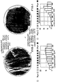
- Figure 1 shows the local distribution of the life values of such Silicon wafer, for comparison purposes the same Si wafer thermally was oxidized and the distribution of the lifetime values is shown in FIG. 5.
- the comparison shows for those treated with the method according to the invention Si disc significantly higher values than for the Si disc with oxidized Surface.
- An average value of 130.1 microseconds results from FIG an average of only 85.84 ⁇ s according to FIG. 5.
- FIG. 6 shows the life values of this Si wafer, which are only as Surface passivation has the so-called natural space oxide, which is why the mean value is also very low, namely only 11.2 ⁇ s.
- the Life distribution according to Figure 2 you get the Life distribution according to Figure 2, the much higher life values shows, namely an average of 150.1 ⁇ s.
- Both Figures 2 and 6 show the same contours indicating the contamination, but because of the larger diffusion length of the minority carriers due to the larger effective Lifetime the contours in Figure 2 are significantly less sharply defined.
- a solution of 73.75 g of isopropanol, 25 g of rosin and 1.25 g of iodine is prepared.
- the pane to be examined is first pickled in a mixture of HF: ENT for 10 s. Approx. 1 ⁇ m silicon is removed. As described above, HF is then pickled, rinsed thoroughly and dried. Then the pane is coated on both sides with the prepared solution by application with a brush at room temperature. After the layer is dry to the touch, the disc is placed in the measuring apparatus.
- the service life values achieved in this way are shown in FIG. 3 and are higher than the values of an Si disk provided with SiO 2 passivation, which FIG. 7 shows.
- the mean value is only 20.75 ⁇ s, which has increased to 109.3 ⁇ s according to FIG. This is an indication of a greater reduction in surface recombination, which in turn means that the value of the volume life that is actually of interest is more precisely determined.
- the method according to the invention can be advantageous in the production of Si components to reduce the surface recombination speed be used.
- FIG. 4 shows a section of an Si wafer 1 into which components for example a transistor 2 with base zone 3 and emitter zone 4 is integrated.
- a Layer 5 applied for example, after the first or second Embodiment is generated and is less than 100 cm / s Surface recombination speed leads.
- this Layer 5 structured using known methods to create a line structure 6, for example to produce aluminum.
- polyimide layer can also be one according to the first or second Embodiment generated layer can be used.
- the advantage of using the layer according to the invention for reduction the surface recombination speed in connection with the production of Si semiconductor devices is that this layer at Temperatures of less than 100 ° C, especially at room temperature can be generated so that the temperature load on the component remains low.
Landscapes
- Chemical & Material Sciences (AREA)
- Engineering & Computer Science (AREA)
- Crystallography & Structural Chemistry (AREA)
- Materials Engineering (AREA)
- Metallurgy (AREA)
- Organic Chemistry (AREA)
- Testing Or Measuring Of Semiconductors Or The Like (AREA)
- Formation Of Insulating Films (AREA)
Description
Hier liegt die Scheibe während der Messung in einer Küvette mit verdünnter HF. Wegen der mit dem Umgang von HF verbundenen Gefahren muß ein relativ großer apparativer Aufwand getrieben werden, um das Bedienungspersonal nicht unnötig zu gefährden.
- Figur 1
- die örtlich Verteilung der Minoritätsträger-Lebensdauer einer mit dem erfindungsgemäßen Verfahren behandelten Siliziumscheibe,
- Figur 2
- die örtliche Verteilung der Minoritäts-Lebensdauer einer mit dem erfindungsgemäßen Verfahren behandelten weiteren Siliziumscheibe,
- Figur 3
- die örtliche Verteilung der Minoritäts-Lebensdauer einer mit dem erfindungsgemäßen Verfahren behandelten weiteren Siliziumscheibe, und
- Figur 4
- eine schematische Schnittdarstellung eines mit dem erfindungsgemäßen Verfahren behandelten Silizium-Bauelementes.
Claims (14)
- Verfahren zur Reduzierung der Oberflächenrekombinationsgeschwindigkeit von Siliziumscheiben, bei dem in der aufgeführten Reihenfolge die Verfahrensschrittea) Reinigen der Siliziumoberfläche, und anschließendesb) Trocknen der Silliziumoberfläche
in normaler Raumatmosphärenumgebung durchgeführt werden und sich daran folgende Verfahrensschritte anschließen:c) Auftragen eines Lackes bei einer Temperatur von weniger als 100°C, undd) Trocknen dieses aufgetragenen Lackes in normaler Raumatmosphäre zur Erzeugung einer elektrisch nichtleitenden Schicht. - Verfahren nach Anspruch 1, dadurch gekennzeichnet, daß ein Lack verwendet wird, der zu einer transparenten Schicht führt.
- Verfahren nach Anspruch 1 oder 2, dadurch gekennzeichnet, daß der Lack bei Raumtemperatur von ca. 25 °C aufgebracht wird.
- Verfahren nach einem der Ansprüche 1 - 3, dadurch gekennzeichnet, daß der Lack eine organische Grundsubstanz aufweist.
- Verfahren nach Anspruch 4, dadurch gekennzeichnet, daß als Grundsubstanz ein natürliches Harz oder ein Alkydharz verwendet wird.
- Verfahren nach Anspruch 5, dadurch gekennzeichnet, daß Kolophonium verwendet wird.
- Verfahren nach Anspruch 5, dadurch gekennzeichnet, daß Alftalat verwendet wird.
- Verfahren nach einem der vorangehenden Ansprüche, dadurch gekennzeichnet, daß die elektrisch nichtleitende Schicht Halogene in Konzentration von mehr als 0,1 Volumen/% enthält.
- Verfahren nach Anspruch 8, dadurch gekennzeichnet, daß als Halogen Jod eingesetzt wird.
- Verfahren nach Anspruch 4 dadurch gekennzeichnet, daß die Grundsubstanz des Lackes im wesentlichen aus Polysiloxanen besteht.
- Verfahren nach einem der vorangehenden Ansprüche, dadurch gekennzeichnet, daß eine weitere Schicht als Passivierungsschicht aufgebracht wird.
- Verfahren nach einem der Ansprüche 1 - 10, dadurch gekennzeichnet, daß eine transparente, nicht leitende Folie auf die Schicht aufgebracht wird.
- Verwendung des Verfahrens nach einem der vorangehenden Ansprüche zur Herstellung von Silizium-Halbleiterbauelementen.
- Verwendung des Verfahrens nach einem der Ansprüche 2 - 12 zur Vorbereitung einer Messung der Minoritätsträgerlebensdauer in Standard-Siliziumscheiben.
Applications Claiming Priority (2)
| Application Number | Priority Date | Filing Date | Title |
|---|---|---|---|
| DE4432294 | 1994-09-12 | ||
| DE4432294A DE4432294A1 (de) | 1994-09-12 | 1994-09-12 | Verfahren zur Reduzierung der Oberflächenrekombinationsgeschwindigkeit in Silizium |
Publications (3)
| Publication Number | Publication Date |
|---|---|
| EP0706207A2 EP0706207A2 (de) | 1996-04-10 |
| EP0706207A3 EP0706207A3 (de) | 1997-07-02 |
| EP0706207B1 true EP0706207B1 (de) | 2002-01-30 |
Family
ID=6527917
Family Applications (1)
| Application Number | Title | Priority Date | Filing Date |
|---|---|---|---|
| EP95113831A Expired - Lifetime EP0706207B1 (de) | 1994-09-12 | 1995-09-04 | Verfahren zur Reduzierung der Oberflächenrekombinationsgeschwindigkeit von Silizium |
Country Status (4)
| Country | Link |
|---|---|
| US (2) | US5972724A (de) |
| EP (1) | EP0706207B1 (de) |
| JP (1) | JPH08107108A (de) |
| DE (2) | DE4432294A1 (de) |
Families Citing this family (4)
| Publication number | Priority date | Publication date | Assignee | Title |
|---|---|---|---|---|
| US6401353B2 (en) * | 2000-03-08 | 2002-06-11 | Dainippon Screen Mfg. Co., Ltd. | Substrate dryer |
| US7491642B2 (en) | 2000-07-12 | 2009-02-17 | The California Institute Of Technology | Electrical passivation of silicon-containing surfaces using organic layers |
| US6836139B2 (en) | 2002-10-22 | 2004-12-28 | Solid State Measurments, Inc. | Method and apparatus for determining defect and impurity concentration in semiconducting material of a semiconductor wafer |
| US7534729B2 (en) * | 2003-02-28 | 2009-05-19 | Board Of Regents, The University Of Texas System | Modification of semiconductor surfaces in a liquid |
Family Cites Families (30)
| Publication number | Priority date | Publication date | Assignee | Title |
|---|---|---|---|---|
| US3115424A (en) * | 1961-04-20 | 1963-12-24 | Int Rectifier Corp | Process for the passivation of semiconductors |
| US3684592A (en) * | 1969-09-30 | 1972-08-15 | Westinghouse Electric Corp | Passivated surfaces and protective coatings for semiconductor devices and processes for producing the same |
| DE2019099C3 (de) * | 1970-04-21 | 1975-11-20 | Licentia Patent-Verwaltungs-Gmbh, 6000 Frankfurt | Verfahren zur Herstellung eines stabilen Oberflachenschutzes fur Halbleiterbauelemente |
| DE2155849C3 (de) * | 1971-11-10 | 1979-07-26 | Semikron Gesellschaft Fuer Gleichrichterbau Und Elektronik Mbh, 8500 Nuernberg | Verfahren zur Herstellung eines stabilisierenden und/oder isolierenden Überzuges auf Halbleiteroberflächen |
| JPS5236817B2 (de) * | 1973-07-27 | 1977-09-19 | ||
| DE3023201A1 (de) * | 1980-06-21 | 1982-01-07 | Hoechst Ag, 6000 Frankfurt | Positiv arbeitendes strahlungsempfindliches gemisch |
| JPS60136310A (ja) * | 1983-12-26 | 1985-07-19 | Hitachi Ltd | レジスト |
| US4608097A (en) * | 1984-10-05 | 1986-08-26 | Exxon Research And Engineering Co. | Method for producing an electronically passivated surface on crystalline silicon using a fluorination treatment and an organic overlayer |
| US4683024A (en) * | 1985-02-04 | 1987-07-28 | American Telephone And Telegraph Company, At&T Bell Laboratories | Device fabrication method using spin-on glass resins |
| US4806504A (en) * | 1986-09-11 | 1989-02-21 | Fairchild Semiconductor Corporation | Planarization method |
| US5270259A (en) * | 1988-06-21 | 1993-12-14 | Hitachi, Ltd. | Method for fabricating an insulating film from a silicone resin using O.sub. |
| US4996254A (en) * | 1988-10-11 | 1991-02-26 | Ethyl Corporation | Production of electronic coatings by spin coating a partially fluorinated polyamic acid composition |
| DE59006874D1 (de) * | 1989-05-31 | 1994-09-29 | Siemens Ag | Verfahren zur Bestimmung der Rekombinationsgeschwindigkeit von Minoritätsträgern an Grenzflächen zwischen Halbleitern und anderen Substanzen. |
| US5262358A (en) * | 1989-11-13 | 1993-11-16 | Fraunhofer-Gesellschaft Zur Forderung Der Angewandten Forschung E.V. | Method for producing a silicate layer in an integrated circuit |
| JP2581268B2 (ja) * | 1990-05-22 | 1997-02-12 | 日本電気株式会社 | 半導体基板の処理方法 |
| CA2017719C (en) * | 1990-05-29 | 1999-01-19 | Zarlink Semiconductor Inc. | Moisture-free sog process |
| JPH04261049A (ja) * | 1991-01-31 | 1992-09-17 | Mitsubishi Electric Corp | 半導体装置およびその製造方法 |
| GB9110566D0 (en) * | 1991-05-16 | 1991-07-03 | Dow Corning Gmbh | Method of coating |
| US5426058A (en) * | 1991-07-12 | 1995-06-20 | Sharp Kabushiki Kaisha | Method of manufacturing solid-state imaging device |
| DE4123900A1 (de) * | 1991-07-18 | 1993-01-21 | Siemens Ag | Schutzschicht fuer wafer |
| JPH05275487A (ja) * | 1991-11-22 | 1993-10-22 | Sumitomo 3M Ltd | 電子部品表面保護材、その表面保護材を備えた電子部品、およびその表面保護材を使用した電子部品の電気的接続方法 |
| US5280184A (en) * | 1992-04-08 | 1994-01-18 | Georgia Tech Research Corporation | Three dimensional integrated circuits with lift-off |
| US5312512A (en) * | 1992-10-23 | 1994-05-17 | Ncr Corporation | Global planarization using SOG and CMP |
| JP3074661B2 (ja) * | 1992-11-20 | 2000-08-07 | 宇部興産株式会社 | ポリイミドシロキサン組成物 |
| US5580828A (en) * | 1992-12-16 | 1996-12-03 | Semiconductor Physics Laboratory Rt | Method for chemical surface passivation for in-situ bulk lifetime measurement of silicon semiconductor material |
| US5391507A (en) * | 1993-09-03 | 1995-02-21 | General Electric Company | Lift-off fabrication method for self-aligned thin film transistors |
| JP3562590B2 (ja) * | 1993-12-01 | 2004-09-08 | 株式会社半導体エネルギー研究所 | 半導体装置作製方法 |
| US5435888A (en) * | 1993-12-06 | 1995-07-25 | Sgs-Thomson Microelectronics, Inc. | Enhanced planarization technique for an integrated circuit |
| US5462898A (en) * | 1994-05-25 | 1995-10-31 | Georgia Tech Research Corporation | Methods for passivating silicon devices at low temperature to achieve low interface state density and low recombination velocity while preserving carrier lifetime |
| US5453406A (en) * | 1994-06-13 | 1995-09-26 | Industrial Technology Research Institute | Aspect ratio independent coating for semiconductor planarization using SOG |
-
1994
- 1994-09-12 DE DE4432294A patent/DE4432294A1/de not_active Withdrawn
-
1995
- 1995-09-04 DE DE59510024T patent/DE59510024D1/de not_active Expired - Lifetime
- 1995-09-04 EP EP95113831A patent/EP0706207B1/de not_active Expired - Lifetime
- 1995-09-11 JP JP7267583A patent/JPH08107108A/ja active Pending
- 1995-09-12 US US08/526,556 patent/US5972724A/en not_active Expired - Lifetime
-
1998
- 1998-11-30 US US09/201,899 patent/US6340642B1/en not_active Expired - Lifetime
Also Published As
| Publication number | Publication date |
|---|---|
| DE4432294A1 (de) | 1996-03-14 |
| EP0706207A3 (de) | 1997-07-02 |
| EP0706207A2 (de) | 1996-04-10 |
| US5972724A (en) | 1999-10-26 |
| US6340642B1 (en) | 2002-01-22 |
| DE59510024D1 (de) | 2002-03-14 |
| JPH08107108A (ja) | 1996-04-23 |
Similar Documents
| Publication | Publication Date | Title |
|---|---|---|
| DE69421014T2 (de) | Widerstandsbestimmungsmethode von N-Typ-Siliziumepitaxieschichten | |
| DE69532060T2 (de) | Vor einer thermischen Behandlung ausgeführtes Reinigungsverfahren | |
| DE1696625C3 (de) | Verfahren zum Erzeugen einer Nitridschutzschicht auf einem Halbleiterkörper | |
| EP0087581B1 (de) | Verfahren zur Herstellung von Siliziumoxidschichten | |
| DE3587238T2 (de) | Planarisierungsverfahren fuer halbleiter und nach diesem verfahren hergestellte strukturen. | |
| DE69010298T2 (de) | Niederdruck/Niedertemperatur-Prozess für Deposition von Siliciumdioxyd. | |
| DE19929239B4 (de) | Verfahren zur Herstellung von MOS-FET-Halbleiterelementen | |
| DE2832740A1 (de) | Verfahren zum herstellen einer halbleitervorrichtung | |
| EP1068646A1 (de) | Verfahren zur einseitigen dotierung eines halbleiterkörpers | |
| DE112017001570B4 (de) | Verfahren zur Bewertung der Reinheit, Verfahren zur Bestimmung des Reinigungszustandes und Verfahren zur Herstellung von Siliciumwafern | |
| DE1489240B1 (de) | Verfahren zum Herstellen von Halbleiterbauelementen | |
| DE1913718A1 (de) | Verfahren zur Herstellung eines Halbleiterbauelements | |
| DE3827496C2 (de) | ||
| DE2550371A1 (de) | Verfahren zum thermischen oxydieren von silicium | |
| EP0706207A2 (de) | Verfahren zur Reduzierung der Oberflächenrekombinationsgeschwindigkeit in Silizium | |
| DE69431148T2 (de) | Methode zur Analyse von Oberflächen verunreinigungen auf Halbleitersubstraten | |
| DE19651778A1 (de) | Verfahren zur Planierung der Oberfläche eines Wafers | |
| EP1086488A2 (de) | Verfahren zum herstellen von halbleiterbauelementen | |
| DE3910185C2 (de) | Siliziumplättchen mit hervorragendem Gettervermögen und Verfahren zu dessen Herstellung | |
| DE4412297C2 (de) | Verfahren zur Rekombinationslebensdauermessung und Vorrichtung zur Durchführung des Verfahrens | |
| DE69329897T2 (de) | Verfahren zur Verbesserung der Eigenschaften der Grenzfläche CaF2 auf Silizium | |
| EP0464372A2 (de) | Verfahren zur Herstellung und Passivierung von Halbleiterbauelementen | |
| DE4234715C1 (de) | Verfahren zur Ermittlung von Halbleitergiften in Quarzglas | |
| WO1998008246A1 (de) | Halbleiterbauelement mit durch ionenimplantation eingebrachten fremdatomen und verfahren zu dessen herstellung________________ | |
| DE4123228C2 (de) | Verfahren zur Dotierstoffkonzentrationsbestimmung mittels Ätzratenbestimmung in Borphosphorsilikatglasschichten für integrierte Halbleiter |
Legal Events
| Date | Code | Title | Description |
|---|---|---|---|
| PUAI | Public reference made under article 153(3) epc to a published international application that has entered the european phase |
Free format text: ORIGINAL CODE: 0009012 |
|
| AK | Designated contracting states |
Kind code of ref document: A2 Designated state(s): DE FR GB IT |
|
| PUAL | Search report despatched |
Free format text: ORIGINAL CODE: 0009013 |
|
| RHK1 | Main classification (correction) |
Ipc: H01L 21/312 |
|
| AK | Designated contracting states |
Kind code of ref document: A3 Designated state(s): DE FR GB IT |
|
| 17P | Request for examination filed |
Effective date: 19970610 |
|
| RAP1 | Party data changed (applicant data changed or rights of an application transferred) |
Owner name: TEMIC SEMICONDUCTOR GMBH |
|
| 17Q | First examination report despatched |
Effective date: 19990623 |
|
| RAP1 | Party data changed (applicant data changed or rights of an application transferred) |
Owner name: ATMEL GERMANY GMBH |
|
| RIC1 | Information provided on ipc code assigned before grant |
Free format text: 7H 01L 21/312 A |
|
| RTI1 | Title (correction) |
Free format text: PROCESS TO REDUCE THE SURFACE RECOMBINATION RATE OF SILICON |
|
| GRAG | Despatch of communication of intention to grant |
Free format text: ORIGINAL CODE: EPIDOS AGRA |
|
| GRAG | Despatch of communication of intention to grant |
Free format text: ORIGINAL CODE: EPIDOS AGRA |
|
| GRAH | Despatch of communication of intention to grant a patent |
Free format text: ORIGINAL CODE: EPIDOS IGRA |
|
| GRAH | Despatch of communication of intention to grant a patent |
Free format text: ORIGINAL CODE: EPIDOS IGRA |
|
| GRAA | (expected) grant |
Free format text: ORIGINAL CODE: 0009210 |
|
| REG | Reference to a national code |
Ref country code: GB Ref legal event code: IF02 |
|
| AK | Designated contracting states |
Kind code of ref document: B1 Designated state(s): DE FR GB IT |
|
| REF | Corresponds to: |
Ref document number: 59510024 Country of ref document: DE Date of ref document: 20020314 |
|
| GBT | Gb: translation of ep patent filed (gb section 77(6)(a)/1977) |
Effective date: 20020407 |
|
| ET | Fr: translation filed | ||
| PLBE | No opposition filed within time limit |
Free format text: ORIGINAL CODE: 0009261 |
|
| STAA | Information on the status of an ep patent application or granted ep patent |
Free format text: STATUS: NO OPPOSITION FILED WITHIN TIME LIMIT |
|
| 26N | No opposition filed | ||
| PGFP | Annual fee paid to national office [announced via postgrant information from national office to epo] |
Ref country code: GB Payment date: 20070914 Year of fee payment: 13 |
|
| PGFP | Annual fee paid to national office [announced via postgrant information from national office to epo] |
Ref country code: IT Payment date: 20070925 Year of fee payment: 13 |
|
| PGFP | Annual fee paid to national office [announced via postgrant information from national office to epo] |
Ref country code: FR Payment date: 20070914 Year of fee payment: 13 |
|
| GBPC | Gb: european patent ceased through non-payment of renewal fee |
Effective date: 20080904 |
|
| REG | Reference to a national code |
Ref country code: FR Ref legal event code: ST Effective date: 20090529 |
|
| PG25 | Lapsed in a contracting state [announced via postgrant information from national office to epo] |
Ref country code: IT Free format text: LAPSE BECAUSE OF NON-PAYMENT OF DUE FEES Effective date: 20080904 |
|
| PG25 | Lapsed in a contracting state [announced via postgrant information from national office to epo] |
Ref country code: FR Free format text: LAPSE BECAUSE OF NON-PAYMENT OF DUE FEES Effective date: 20080930 |
|
| PG25 | Lapsed in a contracting state [announced via postgrant information from national office to epo] |
Ref country code: GB Free format text: LAPSE BECAUSE OF NON-PAYMENT OF DUE FEES Effective date: 20080904 |
|
| PGFP | Annual fee paid to national office [announced via postgrant information from national office to epo] |
Ref country code: DE Payment date: 20090922 Year of fee payment: 15 |
|
| REG | Reference to a national code |
Ref country code: DE Ref legal event code: R119 Ref document number: 59510024 Country of ref document: DE Effective date: 20110401 |
|
| PG25 | Lapsed in a contracting state [announced via postgrant information from national office to epo] |
Ref country code: DE Free format text: LAPSE BECAUSE OF NON-PAYMENT OF DUE FEES Effective date: 20110401 |