EP0698929A2 - Couche réflective arrière, méthode de fabrication, et élément photovoltaique l'utilisant - Google Patents
Couche réflective arrière, méthode de fabrication, et élément photovoltaique l'utilisant Download PDFInfo
- Publication number
- EP0698929A2 EP0698929A2 EP95113240A EP95113240A EP0698929A2 EP 0698929 A2 EP0698929 A2 EP 0698929A2 EP 95113240 A EP95113240 A EP 95113240A EP 95113240 A EP95113240 A EP 95113240A EP 0698929 A2 EP0698929 A2 EP 0698929A2
- Authority
- EP
- European Patent Office
- Prior art keywords
- metal
- layer
- transparent oxide
- back reflector
- reflector layer
- Prior art date
- Legal status (The legal status is an assumption and is not a legal conclusion. Google has not performed a legal analysis and makes no representation as to the accuracy of the status listed.)
- Granted
Links
- 238000000034 method Methods 0.000 title claims abstract description 55
- 229910052751 metal Inorganic materials 0.000 claims abstract description 136
- 239000002184 metal Substances 0.000 claims abstract description 136
- 239000004065 semiconductor Substances 0.000 claims abstract description 54
- 239000000203 mixture Substances 0.000 claims abstract description 37
- 238000004544 sputter deposition Methods 0.000 claims abstract description 22
- 230000008569 process Effects 0.000 claims abstract description 18
- 229910045601 alloy Inorganic materials 0.000 claims abstract description 15
- 239000000956 alloy Substances 0.000 claims abstract description 15
- 239000011261 inert gas Substances 0.000 claims abstract description 12
- 230000015572 biosynthetic process Effects 0.000 claims description 11
- MYMOFIZGZYHOMD-UHFFFAOYSA-N Dioxygen Chemical compound O=O MYMOFIZGZYHOMD-UHFFFAOYSA-N 0.000 claims 1
- 229910001882 dioxygen Inorganic materials 0.000 claims 1
- 238000002310 reflectometry Methods 0.000 abstract description 48
- 238000006243 chemical reaction Methods 0.000 abstract description 25
- 230000003647 oxidation Effects 0.000 abstract description 15
- 238000007254 oxidation reaction Methods 0.000 abstract description 15
- XLOMVQKBTHCTTD-UHFFFAOYSA-N Zinc monoxide Chemical compound [Zn]=O XLOMVQKBTHCTTD-UHFFFAOYSA-N 0.000 description 60
- 239000000758 substrate Substances 0.000 description 42
- XLYOFNOQVPJJNP-UHFFFAOYSA-N water Chemical compound O XLYOFNOQVPJJNP-UHFFFAOYSA-N 0.000 description 37
- 239000007789 gas Substances 0.000 description 35
- 239000010408 film Substances 0.000 description 34
- 239000011787 zinc oxide Substances 0.000 description 29
- 238000000151 deposition Methods 0.000 description 27
- 239000011701 zinc Substances 0.000 description 24
- 230000008021 deposition Effects 0.000 description 21
- 229910021417 amorphous silicon Inorganic materials 0.000 description 19
- 230000000694 effects Effects 0.000 description 15
- 239000010409 thin film Substances 0.000 description 13
- 238000002474 experimental method Methods 0.000 description 12
- 238000004519 manufacturing process Methods 0.000 description 12
- 239000010949 copper Substances 0.000 description 11
- 229910052802 copper Inorganic materials 0.000 description 8
- 238000010248 power generation Methods 0.000 description 8
- 239000011521 glass Substances 0.000 description 7
- 150000002739 metals Chemical class 0.000 description 7
- 239000000523 sample Substances 0.000 description 7
- 239000010935 stainless steel Substances 0.000 description 7
- 229910001220 stainless steel Inorganic materials 0.000 description 7
- XKRFYHLGVUSROY-UHFFFAOYSA-N Argon Chemical compound [Ar] XKRFYHLGVUSROY-UHFFFAOYSA-N 0.000 description 6
- XUIMIQQOPSSXEZ-UHFFFAOYSA-N Silicon Chemical group [Si] XUIMIQQOPSSXEZ-UHFFFAOYSA-N 0.000 description 6
- 229910052782 aluminium Inorganic materials 0.000 description 6
- 229910044991 metal oxide Inorganic materials 0.000 description 6
- 150000004706 metal oxides Chemical class 0.000 description 6
- 229910052709 silver Inorganic materials 0.000 description 6
- QVGXLLKOCUKJST-UHFFFAOYSA-N atomic oxygen Chemical compound [O] QVGXLLKOCUKJST-UHFFFAOYSA-N 0.000 description 5
- 239000013078 crystal Substances 0.000 description 5
- 230000007423 decrease Effects 0.000 description 5
- 238000011156 evaluation Methods 0.000 description 5
- 230000001788 irregular Effects 0.000 description 5
- 238000001755 magnetron sputter deposition Methods 0.000 description 5
- 239000000463 material Substances 0.000 description 5
- 239000001301 oxygen Substances 0.000 description 5
- 229910052760 oxygen Inorganic materials 0.000 description 5
- 229910052710 silicon Inorganic materials 0.000 description 5
- 239000010703 silicon Substances 0.000 description 5
- XOLBLPGZBRYERU-UHFFFAOYSA-N tin dioxide Chemical compound O=[Sn]=O XOLBLPGZBRYERU-UHFFFAOYSA-N 0.000 description 5
- RYGMFSIKBFXOCR-UHFFFAOYSA-N Copper Chemical compound [Cu] RYGMFSIKBFXOCR-UHFFFAOYSA-N 0.000 description 4
- XEEYBQQBJWHFJM-UHFFFAOYSA-N Iron Chemical compound [Fe] XEEYBQQBJWHFJM-UHFFFAOYSA-N 0.000 description 4
- BLRPTPMANUNPDV-UHFFFAOYSA-N Silane Chemical compound [SiH4] BLRPTPMANUNPDV-UHFFFAOYSA-N 0.000 description 4
- 229910000577 Silicon-germanium Inorganic materials 0.000 description 4
- 230000003247 decreasing effect Effects 0.000 description 4
- 230000002708 enhancing effect Effects 0.000 description 4
- 230000001965 increasing effect Effects 0.000 description 4
- QTBSBXVTEAMEQO-UHFFFAOYSA-N Acetic acid Chemical compound CC(O)=O QTBSBXVTEAMEQO-UHFFFAOYSA-N 0.000 description 3
- BQCADISMDOOEFD-UHFFFAOYSA-N Silver Chemical compound [Ag] BQCADISMDOOEFD-UHFFFAOYSA-N 0.000 description 3
- HCHKCACWOHOZIP-UHFFFAOYSA-N Zinc Chemical compound [Zn] HCHKCACWOHOZIP-UHFFFAOYSA-N 0.000 description 3
- 230000009471 action Effects 0.000 description 3
- XAGFODPZIPBFFR-UHFFFAOYSA-N aluminium Chemical compound [Al] XAGFODPZIPBFFR-UHFFFAOYSA-N 0.000 description 3
- 230000003064 anti-oxidating effect Effects 0.000 description 3
- 229910052786 argon Inorganic materials 0.000 description 3
- 238000010438 heat treatment Methods 0.000 description 3
- 230000035945 sensitivity Effects 0.000 description 3
- 239000004332 silver Substances 0.000 description 3
- 230000003595 spectral effect Effects 0.000 description 3
- 229910052725 zinc Inorganic materials 0.000 description 3
- CURLTUGMZLYLDI-UHFFFAOYSA-N Carbon dioxide Chemical compound O=C=O CURLTUGMZLYLDI-UHFFFAOYSA-N 0.000 description 2
- UFHFLCQGNIYNRP-UHFFFAOYSA-N Hydrogen Chemical compound [H][H] UFHFLCQGNIYNRP-UHFFFAOYSA-N 0.000 description 2
- 229910020328 SiSn Inorganic materials 0.000 description 2
- 230000015556 catabolic process Effects 0.000 description 2
- 239000000919 ceramic Substances 0.000 description 2
- 238000000354 decomposition reaction Methods 0.000 description 2
- 238000006731 degradation reaction Methods 0.000 description 2
- 239000002803 fossil fuel Substances 0.000 description 2
- 239000001257 hydrogen Substances 0.000 description 2
- 229910052739 hydrogen Inorganic materials 0.000 description 2
- 230000006872 improvement Effects 0.000 description 2
- PJXISJQVUVHSOJ-UHFFFAOYSA-N indium(III) oxide Inorganic materials [O-2].[O-2].[O-2].[In+3].[In+3] PJXISJQVUVHSOJ-UHFFFAOYSA-N 0.000 description 2
- 238000007733 ion plating Methods 0.000 description 2
- 229910052742 iron Inorganic materials 0.000 description 2
- 238000005259 measurement Methods 0.000 description 2
- 229910021424 microcrystalline silicon Inorganic materials 0.000 description 2
- 230000003287 optical effect Effects 0.000 description 2
- 230000006798 recombination Effects 0.000 description 2
- 238000005215 recombination Methods 0.000 description 2
- 230000009467 reduction Effects 0.000 description 2
- 238000002834 transmittance Methods 0.000 description 2
- 241000282414 Homo sapiens Species 0.000 description 1
- BUGBHKTXTAQXES-UHFFFAOYSA-N Selenium Chemical compound [Se] BUGBHKTXTAQXES-UHFFFAOYSA-N 0.000 description 1
- 241000872198 Serjania polyphylla Species 0.000 description 1
- VYPSYNLAJGMNEJ-UHFFFAOYSA-N Silicium dioxide Chemical compound O=[Si]=O VYPSYNLAJGMNEJ-UHFFFAOYSA-N 0.000 description 1
- 229910017875 a-SiN Inorganic materials 0.000 description 1
- 238000010521 absorption reaction Methods 0.000 description 1
- 238000000137 annealing Methods 0.000 description 1
- 229910052799 carbon Inorganic materials 0.000 description 1
- 239000001569 carbon dioxide Substances 0.000 description 1
- 229910002092 carbon dioxide Inorganic materials 0.000 description 1
- 230000008859 change Effects 0.000 description 1
- 238000005229 chemical vapour deposition Methods 0.000 description 1
- 239000003245 coal Substances 0.000 description 1
- 150000001875 compounds Chemical class 0.000 description 1
- 239000004020 conductor Substances 0.000 description 1
- 238000010924 continuous production Methods 0.000 description 1
- 230000007547 defect Effects 0.000 description 1
- 230000001419 dependent effect Effects 0.000 description 1
- 238000009792 diffusion process Methods 0.000 description 1
- 238000010894 electron beam technology Methods 0.000 description 1
- 238000005516 engineering process Methods 0.000 description 1
- 238000001704 evaporation Methods 0.000 description 1
- QUZPNFFHZPRKJD-UHFFFAOYSA-N germane Chemical compound [GeH4] QUZPNFFHZPRKJD-UHFFFAOYSA-N 0.000 description 1
- 229910052986 germanium hydride Inorganic materials 0.000 description 1
- 238000000227 grinding Methods 0.000 description 1
- -1 i.e. Substances 0.000 description 1
- 239000012535 impurity Substances 0.000 description 1
- 229910052738 indium Inorganic materials 0.000 description 1
- APFVFJFRJDLVQX-UHFFFAOYSA-N indium atom Chemical compound [In] APFVFJFRJDLVQX-UHFFFAOYSA-N 0.000 description 1
- 230000031700 light absorption Effects 0.000 description 1
- 230000007774 longterm Effects 0.000 description 1
- 238000000059 patterning Methods 0.000 description 1
- 239000003208 petroleum Substances 0.000 description 1
- 230000010363 phase shift Effects 0.000 description 1
- 238000007747 plating Methods 0.000 description 1
- 238000012545 processing Methods 0.000 description 1
- 230000005855 radiation Effects 0.000 description 1
- 238000012827 research and development Methods 0.000 description 1
- 239000011347 resin Substances 0.000 description 1
- 229920005989 resin Polymers 0.000 description 1
- 238000005096 rolling process Methods 0.000 description 1
- 238000004088 simulation Methods 0.000 description 1
- 238000009751 slip forming Methods 0.000 description 1
- 238000001228 spectrum Methods 0.000 description 1
- 238000003860 storage Methods 0.000 description 1
- 239000000126 substance Substances 0.000 description 1
- 238000002230 thermal chemical vapour deposition Methods 0.000 description 1
- 229910001887 tin oxide Inorganic materials 0.000 description 1
- 238000001771 vacuum deposition Methods 0.000 description 1
- 238000010792 warming Methods 0.000 description 1
- 238000004804 winding Methods 0.000 description 1
Images


Classifications
-
- H—ELECTRICITY
- H01—ELECTRIC ELEMENTS
- H01L—SEMICONDUCTOR DEVICES NOT COVERED BY CLASS H10
- H01L31/00—Semiconductor devices sensitive to infrared radiation, light, electromagnetic radiation of shorter wavelength or corpuscular radiation and specially adapted either for the conversion of the energy of such radiation into electrical energy or for the control of electrical energy by such radiation; Processes or apparatus specially adapted for the manufacture or treatment thereof or of parts thereof; Details thereof
- H01L31/04—Semiconductor devices sensitive to infrared radiation, light, electromagnetic radiation of shorter wavelength or corpuscular radiation and specially adapted either for the conversion of the energy of such radiation into electrical energy or for the control of electrical energy by such radiation; Processes or apparatus specially adapted for the manufacture or treatment thereof or of parts thereof; Details thereof adapted as photovoltaic [PV] conversion devices
- H01L31/054—Optical elements directly associated or integrated with the PV cell, e.g. light-reflecting means or light-concentrating means
- H01L31/056—Optical elements directly associated or integrated with the PV cell, e.g. light-reflecting means or light-concentrating means the light-reflecting means being of the back surface reflector [BSR] type
-
- H—ELECTRICITY
- H01—ELECTRIC ELEMENTS
- H01L—SEMICONDUCTOR DEVICES NOT COVERED BY CLASS H10
- H01L31/00—Semiconductor devices sensitive to infrared radiation, light, electromagnetic radiation of shorter wavelength or corpuscular radiation and specially adapted either for the conversion of the energy of such radiation into electrical energy or for the control of electrical energy by such radiation; Processes or apparatus specially adapted for the manufacture or treatment thereof or of parts thereof; Details thereof
- H01L31/02—Details
- H01L31/0236—Special surface textures
- H01L31/02363—Special surface textures of the semiconductor body itself, e.g. textured active layers
-
- H—ELECTRICITY
- H01—ELECTRIC ELEMENTS
- H01L—SEMICONDUCTOR DEVICES NOT COVERED BY CLASS H10
- H01L31/00—Semiconductor devices sensitive to infrared radiation, light, electromagnetic radiation of shorter wavelength or corpuscular radiation and specially adapted either for the conversion of the energy of such radiation into electrical energy or for the control of electrical energy by such radiation; Processes or apparatus specially adapted for the manufacture or treatment thereof or of parts thereof; Details thereof
- H01L31/02—Details
- H01L31/0236—Special surface textures
- H01L31/02366—Special surface textures of the substrate or of a layer on the substrate, e.g. textured ITO/glass substrate or superstrate, textured polymer layer on glass substrate
-
- H—ELECTRICITY
- H01—ELECTRIC ELEMENTS
- H01L—SEMICONDUCTOR DEVICES NOT COVERED BY CLASS H10
- H01L31/00—Semiconductor devices sensitive to infrared radiation, light, electromagnetic radiation of shorter wavelength or corpuscular radiation and specially adapted either for the conversion of the energy of such radiation into electrical energy or for the control of electrical energy by such radiation; Processes or apparatus specially adapted for the manufacture or treatment thereof or of parts thereof; Details thereof
- H01L31/0248—Semiconductor devices sensitive to infrared radiation, light, electromagnetic radiation of shorter wavelength or corpuscular radiation and specially adapted either for the conversion of the energy of such radiation into electrical energy or for the control of electrical energy by such radiation; Processes or apparatus specially adapted for the manufacture or treatment thereof or of parts thereof; Details thereof characterised by their semiconductor bodies
- H01L31/036—Semiconductor devices sensitive to infrared radiation, light, electromagnetic radiation of shorter wavelength or corpuscular radiation and specially adapted either for the conversion of the energy of such radiation into electrical energy or for the control of electrical energy by such radiation; Processes or apparatus specially adapted for the manufacture or treatment thereof or of parts thereof; Details thereof characterised by their semiconductor bodies characterised by their crystalline structure or particular orientation of the crystalline planes
- H01L31/0392—Semiconductor devices sensitive to infrared radiation, light, electromagnetic radiation of shorter wavelength or corpuscular radiation and specially adapted either for the conversion of the energy of such radiation into electrical energy or for the control of electrical energy by such radiation; Processes or apparatus specially adapted for the manufacture or treatment thereof or of parts thereof; Details thereof characterised by their semiconductor bodies characterised by their crystalline structure or particular orientation of the crystalline planes including thin films deposited on metallic or insulating substrates ; characterised by specific substrate materials or substrate features or by the presence of intermediate layers, e.g. barrier layers, on the substrate
- H01L31/03921—Semiconductor devices sensitive to infrared radiation, light, electromagnetic radiation of shorter wavelength or corpuscular radiation and specially adapted either for the conversion of the energy of such radiation into electrical energy or for the control of electrical energy by such radiation; Processes or apparatus specially adapted for the manufacture or treatment thereof or of parts thereof; Details thereof characterised by their semiconductor bodies characterised by their crystalline structure or particular orientation of the crystalline planes including thin films deposited on metallic or insulating substrates ; characterised by specific substrate materials or substrate features or by the presence of intermediate layers, e.g. barrier layers, on the substrate including only elements of Group IV of the Periodic Table
-
- H—ELECTRICITY
- H01—ELECTRIC ELEMENTS
- H01L—SEMICONDUCTOR DEVICES NOT COVERED BY CLASS H10
- H01L31/00—Semiconductor devices sensitive to infrared radiation, light, electromagnetic radiation of shorter wavelength or corpuscular radiation and specially adapted either for the conversion of the energy of such radiation into electrical energy or for the control of electrical energy by such radiation; Processes or apparatus specially adapted for the manufacture or treatment thereof or of parts thereof; Details thereof
- H01L31/18—Processes or apparatus specially adapted for the manufacture or treatment of these devices or of parts thereof
- H01L31/1884—Manufacture of transparent electrodes, e.g. TCO, ITO
-
- H—ELECTRICITY
- H01—ELECTRIC ELEMENTS
- H01L—SEMICONDUCTOR DEVICES NOT COVERED BY CLASS H10
- H01L31/00—Semiconductor devices sensitive to infrared radiation, light, electromagnetic radiation of shorter wavelength or corpuscular radiation and specially adapted either for the conversion of the energy of such radiation into electrical energy or for the control of electrical energy by such radiation; Processes or apparatus specially adapted for the manufacture or treatment thereof or of parts thereof; Details thereof
- H01L31/18—Processes or apparatus specially adapted for the manufacture or treatment of these devices or of parts thereof
- H01L31/20—Processes or apparatus specially adapted for the manufacture or treatment of these devices or of parts thereof such devices or parts thereof comprising amorphous semiconductor materials
- H01L31/206—Particular processes or apparatus for continuous treatment of the devices, e.g. roll-to roll processes, multi-chamber deposition
-
- Y—GENERAL TAGGING OF NEW TECHNOLOGICAL DEVELOPMENTS; GENERAL TAGGING OF CROSS-SECTIONAL TECHNOLOGIES SPANNING OVER SEVERAL SECTIONS OF THE IPC; TECHNICAL SUBJECTS COVERED BY FORMER USPC CROSS-REFERENCE ART COLLECTIONS [XRACs] AND DIGESTS
- Y02—TECHNOLOGIES OR APPLICATIONS FOR MITIGATION OR ADAPTATION AGAINST CLIMATE CHANGE
- Y02E—REDUCTION OF GREENHOUSE GAS [GHG] EMISSIONS, RELATED TO ENERGY GENERATION, TRANSMISSION OR DISTRIBUTION
- Y02E10/00—Energy generation through renewable energy sources
- Y02E10/50—Photovoltaic [PV] energy
- Y02E10/52—PV systems with concentrators
-
- Y—GENERAL TAGGING OF NEW TECHNOLOGICAL DEVELOPMENTS; GENERAL TAGGING OF CROSS-SECTIONAL TECHNOLOGIES SPANNING OVER SEVERAL SECTIONS OF THE IPC; TECHNICAL SUBJECTS COVERED BY FORMER USPC CROSS-REFERENCE ART COLLECTIONS [XRACs] AND DIGESTS
- Y02—TECHNOLOGIES OR APPLICATIONS FOR MITIGATION OR ADAPTATION AGAINST CLIMATE CHANGE
- Y02E—REDUCTION OF GREENHOUSE GAS [GHG] EMISSIONS, RELATED TO ENERGY GENERATION, TRANSMISSION OR DISTRIBUTION
- Y02E10/00—Energy generation through renewable energy sources
- Y02E10/50—Photovoltaic [PV] energy
- Y02E10/548—Amorphous silicon PV cells
-
- Y—GENERAL TAGGING OF NEW TECHNOLOGICAL DEVELOPMENTS; GENERAL TAGGING OF CROSS-SECTIONAL TECHNOLOGIES SPANNING OVER SEVERAL SECTIONS OF THE IPC; TECHNICAL SUBJECTS COVERED BY FORMER USPC CROSS-REFERENCE ART COLLECTIONS [XRACs] AND DIGESTS
- Y02—TECHNOLOGIES OR APPLICATIONS FOR MITIGATION OR ADAPTATION AGAINST CLIMATE CHANGE
- Y02P—CLIMATE CHANGE MITIGATION TECHNOLOGIES IN THE PRODUCTION OR PROCESSING OF GOODS
- Y02P70/00—Climate change mitigation technologies in the production process for final industrial or consumer products
- Y02P70/50—Manufacturing or production processes characterised by the final manufactured product
Definitions
- the present invention concerns a back reflector layer, a method for forming it, a photovoltaic element using it, and a process for fabricating the photovoltaic element.
- the invention relates to a back reflector layer having a high reflectivity and an asperity structure (hereinafter referred to as a texture structure), and a photovoltaic element high in performance, high in reliability, and capable of being mass-produced.
- Single-crystal or polycrystal silicon groups have popularly been used heretofore for the solar cells for solar-electric power generation.
- growth of crystal necessitates a lot of energy and time, and complex steps are necessary after the growth. Thus, they are not suitable for mass production, and it is difficult to provide them at low price.
- active research and development have been made on the so-called thin-film semiconductor solar cells using amorphous silicon (hereinafter referred to as a-Si) and compound semiconductors such as CdS and CuInSe2.
- One of them is to provide a back reflector layer for enhancing the reflectivity of light on the surface of substrate in order to bring the light energy such as the sunlight not absorbed by the thin-film semiconductor for photoelectric conversion back again to the thin-film semiconductor, i.e., in order to effectively utilize incident light.
- the substrate is optically transparent and the sunlight is made incident from the substrate side
- an electrode is formed on the surface thereof, using a metal with high reflectivity such as silver (Ag), aluminum (Al), or copper (Cu).
- a layer of the same metal as listed above is first formed on the substrate and then the semiconductor layer is formed thereon.
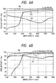
- the reflectivity can be more enhanced by the multiple interference effect when a transparent layer having appropriate optical properties is interposed between the metal layer and the thin-film semiconductor layer, for example as shown in Figs. 6A and 6B.
- Figs. 6A and 6B show simulation results to verify that the reflectivity is improved when zinc oxide (ZnO) is interposed as a transparent layer between silicon and a metal selected from the listed metals:
- Fig. 6A shows reflectivities when a-Si is formed on the metals;
- Fig. 6B shows reflectivities when ZnO is formed on the metals and then a-Si is formed on ZnO.
- Japanese Patent Publication No. 60-41878 includes such description that use of a transparent layer can prevent the semiconductor and the metal layer from forming an alloy.
- United States Patents No. 4,532,372 and No. 4,598,306 describe that use of a transparent layer with an appropriate resistance can prevent an excessive electric current from flowing between the electrodes even if the semiconductor layer has a short-circuited portion.
- Another idea to enhance the conversion efficiency of solar cell is a method (of the texture structure) for making fine asperities on the surface of solar cell and/or an interface between the back reflector layer and the semiconductor layer.
- the sunlight is scattered by the surface of solar cell and/or the interface between the back reflector layer and the semiconductor layer and further is confined inside the semiconductor (which is the light trap effect), whereby the sunlight can be effectively absorbed in the semiconductor.
- a good result can be obtained by texturing the surface of the transparent electrode such as tin oxide (SnO2) on the substrate.
- a good result can be obtained by texturing the surface of the metal layer used as the back reflector layer.
- Fig. 7 shows an example in which absorption of incident light increases by use of the back, reflector layer in such a texture structure.
- curve (a) represents a spectral sensitivity of an a-Si solar cell using a flat Ag layer as the metal layer
- a curve (b) a spectral sensitivity of an a-Si solar cell fabricated in the same manner as it except that an Ag layer is formed in the texture structure as the metal layer.
- One of methods for obtaining the texture structure of transparent layer is the method for introducing water vapor into discharge gas (Effect of Water Vapor on the Textured ZnO-Based Films for Solar Cells by DC-Magnetron Sputtering; Tokio Nakada, Yukinobu Ohkubo and Akio Kunioka (Japanese Journal of Applied Physics Vol. 30 No 12A, December 1991, pp. 3344-3348)). Observation by SEM confirmed that the texture structure was more developed by the method for depositing a metal oxide on a glass plate as introducing water vapor than by a method for depositing the metal oxide using Ar gas as a discharge gas. Although the conventional technology required a thick film in order to obtain a necessary texture structure for raising the characteristics of solar cell, this method made it possible to decrease the film thickness.
- An object of the present invention is to provide a back reflector layer which is a transparent and electrically conductive film with the texture structure on a ground metal or alloy layer, and a method for producing it.
- a further object of the invention is to provide a photovoltaic element excellent in characteristics such as the conversion efficiency, and a process for fabricating it.
- a back reflector layer of the present invention is a back reflector layer having a metal or alloy (hereinafter referred to as a first metal), and a transparent oxide comprising a second metal and formed on the first metal, wherein an electron affinity of the second metal is 0.46 or more eV smaller than that of the first metal and wherein the transparent oxide is formed by a sputtering method in an atmosphere comprising at least H2O and an inert gas and with a target having a composition ratio of the second metal being 1.06 to 1.2 times a stoichiometric composition thereof.
- a metal or alloy hereinafter referred to as a first metal
- a transparent oxide comprising a second metal and formed on the first metal, wherein an electron affinity of the second metal is 0.46 or more eV smaller than that of the first metal and wherein the transparent oxide is formed by a sputtering method in an atmosphere comprising at least H2O and an inert gas and with a target having a composition ratio of the second metal being 1.06
- the film thickness of the transparent oxide of the second metal is preferably between 5 nm and 20 nm, and a second transparent oxide is preferably further formed on the transparent oxide by a sputtering method using a target with a composition ratio of the second metal being 0.96 to 1.04 times the stoichiometric composition thereof.
- a photovoltaic element of the present invention is featured in that a semiconductor junction is formed on the above back reflector layer.
- a method for forming the back reflector layer is one in which on a metal or alloy (hereinafter referred to as a first metal) there is formed a transparent oxide of a second metal having an electron affinity 0.46 or more eV smaller than that of the first metal, wherein the transparent oxide is formed by a sputtering method in an atmosphere comprising at least H2O and an inert gas and with a target having a composition ratio of the second metal being 1.06 to 1.2 times a stoichiometric composition thereof.
- a metal or alloy hereinafter referred to as a first metal
- the film thickness of the transparent oxide is preferably between 5 nm and 20 nm, and another transparent oxide is preferably formed after formation of the above transparent oxide, using a target having a composition ratio of the second metal being 0.96 to 1.04 times the stoichiometric composition thereof.
- O2 gas is preferably added into the above atmosphere.
- a process for fabricating the photovoltaic element of the present invention is featured in that a semiconductor junction is formed after formation of the above back reflector layer. This process can form the photovoltaic element having excellent characteristics.
- the present inventor found the following problems in the cases where a back reflector layer of a transparent and electrically conductive layer having the texture structure was formed on a metal layer, using H2O as a reactive gas.
- H2O a reactive gas
- the texture was developed in even smaller thicknesses than in case of a discharge gas including only an inert gas such as Ar, but the inventor observed such a tendency that the ground layer, the metal or alloy film, was oxidized. It was found that this oxidation lowered the reflectivity, resulting in lowering the function of the back reflector layer for photoelectric conversion element.
- the ground metal or alloy layer is subjected to oxidation by the H2O or O2 gas in the atmosphere.
- the inventor of the present application found out after intensive and extensive studies that the transparent oxide with asperity was capable of being formed while preventing the oxidation of the ground metal upon sputtering and by the transparent oxide if a metal having an electron affinity 0.46 or more eV smaller than that of the ground metal (first metal) was selected as a metal (second metal) composing the transparent oxide and if the transparent oxide was formed using a target containing the metal 1.06 to 1.2 times more than the stoichiometric composition of the transparent oxide.
- the electron affinity is defined as follows. In a reaction where an atom or molecule A is coupled with an electron to form a negative ion, energy discharged at that time is defined as an electron affinity of A. Electrons become easier to move as this energy of one atom or molecule becomes smaller than that of another atom or molecule. Accordingly, using the target having a more content of the second metal than the stoichiometric composition of the transparent oxide layer, the transparent oxide layer is formed in an excessive amount of the second metal component. Thus, even if the ground metal layer is oxidized upon sputtering, the excessive second metal in the metal oxide deposited thereon can deprive the ground metal layer of oxygen. Or, it is considered that the excessive second metal is oxidized before oxidation of the ground metal layer, thereby preventing oxidation of the ground metal layer.
- the target used in forming the transparent oxide is determined to have the metal composition ratio of 1.06 to 1.2 times the stoichiometric composition.
- FIG. 1A - 1C are diagrammatic drawings to show fabrication steps of the photovoltaic element of the present invention.
- reference numeral 101 designates a substrate, and a layer 102 of a metal with high reflectivity is formed on the surface of the substrate. If the substrate 101 itself is made of a material being electrically conductive and having a sufficiently high reflectivity, the metal layer 102 may be omitted. Here, at least the surface of the metal layer 102 is preferably formed as a flat surface in order to enhance the reflectivity (Fig. 1A).
- a transparent oxide layer 103 having fine asperities on the surface is formed on the metal layer 102.
- This example shows a case of ZnO being used as the transparent oxide layer 103.
- This example shows a case where the transparent oxide layer 103 is composed of first and second transparent oxide layers, which are a metal oxide layer (first transparent oxide layer) 104, formed using a metal-excessive target (Zn + ZnO), and a metal oxide layer (second transparent oxide layer) 105, formed using a ZnO target.
- reference numeral 201 designates a deposition chamber, which is arranged to be evacuated to the vacuum by an exhaust pump not shown. Inside the deposition chamber, H2O and an inert gas such as argon (Ar) are introduced at predetermined flow rates to realize a desired mixture ratio thereof through gas inlet pipes 202a, 202b connected to gas bombs not shown, and an aperture of an exhaust valve 203 is adjusted to keep the inside of the deposition chamber 201 at a predetermined pressure.
- an inert gas such as argon (Ar)
- a substrate 204 having the flat metal layer 102 on the surface is fixed to a surface of anode 206 in which a heater 205 is installed.
- a cathode electrode 208 Disposed as opposed to the anode 206 is a cathode electrode 208, to a surface of which a target 207 is fixed and inside which a magnet not shown is provided.
- the target 207 is, for example, zinc oxide containing 56 % of zinc.
- a power supply 209 applies a high voltage of direct current (DC) to the cathode electrode 208 to produce plasma 210 between the cathode and the anode. An action of this plasma 210 generates active oxygen, which temporarily oxidizes the metal layer 102.
- DC direct current
- ZnO and Zn as the second metal with an electron affinity 0.46 or more eV smaller than that of the first metal used in the metal layer 102, in the target 207 are deposited on the substrate 204, and the thus deposited Zn as the second metal deprives the metal layer 102 oxidized, of oxygen to reduce the metal layer 102. Accordingly, the metal layer 102 maintains a high reflectivity, and the second metal depriving of oxygen serves as a transparent oxide layer.
- the target is changed to a ZnO target, for example, containing 50 % zinc, and a second transparent oxide is deposited on the first transparent oxide.
- the transparent oxide 103 is transparent to light energy transmitted by a semiconductor. Further, it has an appropriate electric resistance and the surface thereof is of the texture structure. Particularly, use of water vapor as a reactive gas develops the texture structure in the same film thickness more than in the case of a discharge gas containing only the inert gas such as Ar (Fig. 1B).
- a semiconductor 106 is formed on the transparent oxide 103.
- Fig. 1C shows an example to use a pin-type a-Si semiconductor as a semiconductor junction.
- reference numeral 107 is an n-type a-Si semiconductor, 108 an i-type a-Si semiconductor, and 109 a p-type a-Si semiconductor.
- the photoelectric conversion portion may be formed using the pn junction or Schottky junction as the semiconductor 106.
- a method for forming the semiconductor may be selected from a variety of methods including the RFCVD process, the MWCVD process, the photo-assisted CVD process, the thermal CVD process, the sputtering process, the ion plating process, etc. If the semiconductor 106 is thin enough, the entire semiconductor junction often shows the texture structure similar to the transparent oxide 103, as shown in Fig. 1C.
- a transparent electrode 110 such as ITO or SnO2 is used where the light is made incident from the opposite side to the substrate.
- a collector electrode 111, a bus-bar, or the like may be provided in a desired shape (for example, in a comb shape).
- the photovoltaic element fabricated by the above procedures has the following advantages.
- a scanning probe microscope (Nano Scope III manufactured by Desital Instruments Co.) was used to obtain a texture degree (average height of differences between crests and roots). The results are shown in Table 1.
- the total reflectivity indicates a rate of intensity of light reflected in all directions relative to the intensity of incident light
- the irregular reflectivity indicates a rate of intensity of reflected light except for the light in the directions of reflecting angles relative to the intensity of incident light.
- the texture degree increased as the rate of H2O increased, similarly as in the results of Experiment 1, but the total reflectivity decreased with increase of H2O.
- Samples were etched with acetic acid to observe the surface of Ag. The observation confirmed that the surface of Ag was oxidized to become black. From this, it is seen that H2O in the discharge gas is activated by discharge to promote oxidation of the surface of Ag. The metal layer continues becoming black with introduction of H2O.
- the texture degree is not so large until the ratio of 80:20.
- the texture degree steeply increases from the ratio of 70:30 and then saturates soon, thus decreasing the irregular reflectivity.
- composition ratios of target are results of measurement by XMA (energy dispersive x-ray analyzer EMAX-5770 manufactured by Horiba Seisakusho). Also, R in the table represents a ratio of Zn composition in the target relative to the stoichiometric composition.
- the total reflectivity took great values when the first transparent oxide had a film thickness of not less than 2 nm. This assures that the first transparent oxide is effectively functioning as an antioxidation layer if the film thickness is not less than 2 nm. With a further increase in film thickness, a color of Zn as a metal becomes outstanding, thereby decreasing the reflectivity. It is thus seen that the Zn + ZnO layer for antioxidation of the Ag layer needs to be used in an appropriate range of film thickness because of its properties. As apparent from the table, the film thickness of the first transparent oxide is more preferably 5 - 20 nm.
- the reflectivity was measured using the various types of back reflector layers. The results are also shown in Table 5.
- ⁇ represents a total reflectivity of not less than 70 %, while X does a total reflectivity of less than 70 %.
- Table 6 shows electron affinities of the respective elements listed (from Revised Third Edition of Handbook of Chemistry, Foundations II, compiled by the Chemical Society of Japan and published by Maruzen). Further, Table 7 shows values indicating differences, E (A) - E(B), in electron affinity between the metals used in the metal layer and the metals used in the transparent layer.
- an a-Si layer with the n-type conductivity was deposited in 20 nm with raw gases of SiH4 and PH3, an a-SiGe layer with the i-type conductivity in 400 nm with raw gases of SiH4 and GeH4, and a microcrystalline ( ⁇ c) Si layer with the p-type conductivity in 10 nm with raw gases of SiH4, BF3, and H2, in the named order by the glow discharge decomposition method to form semiconductor junctions. (Since a-Si formed by the glow discharge decomposition method of SiH4 etc.
- Sample 6b was prepared in the same manner as Sample 6a except that the film thickness of the transparent oxide was 800 nm. Further, Samples 6c and 6d were prepared in the same manner as Samples 6a and 6b except that the discharge gas was Ar and H2O at a ratio of 1:1.
- a variety of metals can be suitably applicable to the substrate 101. From among them, a stainless steel plate, a galvanized sheet iron, an aluminum plate, a copper plate, and the like are preferably applicable because of relatively low prices. These metal plates may be used in a certain cut shape or in the form of an elongate sheet depending upon the thickness of plate. In the case of the sheet form, because the sheet plate can be rolled in a coil form, it well matches continuous production and facilitates storage and transportation.
- the substrate may be a crystal substrate of silicon etc., a glass or ceramic plate, or a plate of a resin etc. The surface of the substrate may be ground, but it may be used without grinding if finishing is acceptably fine, for example like a stainless steel plate treated by bright annealing.
- the substrate is one with low reflectivity of light when not treated, for example like the stainless steel plate or galvanized sheet iron, or an insulating substrate such as glass, it is preferably used after depositing a metal with high reflectivity such as silver, aluminum, or copper on the substrate.
- a metal with high reflectivity such as silver, aluminum, or copper
- the reflectivity is high for the light of longer wavelengths than those. What wavelength is to be determined as a border for high reflectivities depends upon the light absorption coefficient and the film thickness of the semiconductor used.
- the border wavelength is about 600 nm, and thus, copper can be suitably used (Figs. 6A and 6B). Further, even the materials with low electric conduction when untreated, like glass or ceramics, can be used as the substrate by forming a metal layer thereon.
- Deposition of the metal layer can be effected by either one selected from the vacuum deposition by resistance heating or electron beam, the sputtering method, the ion plating method, the various CVD methods utilizing plasma, light, and thermal energy, the plating method, etc.
- a case of the sputtering method is explained.
- Fig. 3 shows an example of a sputtering apparatus.
- Reference numeral 301 designates a deposition chamber, which is arranged to be evacuated to the vacuum by an exhaust pump not shown.
- an inert gas such as argon (Ar) is introduced at a predetermined flow rate through a gas inlet pipe 302 connected to a gas bomb not shown, and an aperture of an exhaust valve 303 is adjusted to keep the inside of the deposition chamber 301 at a predetermined pressure.
- the substrate 304 is fixed to the surface of anode 306, inside which a heater 305 is provided.
- a cathode electrode 308, to the surface of which a target 307 is fixed, is arranged as opposed to the anode 306.
- the target 307 is a block of a metal to be deposited.
- the cathode electrode is connected to a power supply 309.
- the power supply 309 applies a high voltage of radio frequency (RF) or direct current (DC) to produce plasma 310 between the cathode and the anode.
- RF radio frequency
- DC direct current
- An action of this plasma makes metal atoms in the target 307 deposited on the substrate 304.
- the deposition rate can be enhanced by the magnetron sputtering apparatus increased in intensity of plasma by setting a magnet inside the cathode 308.
- the former target can be fabricated by the normal method, but the latter target requires a change of the fabrication conditions.
- press hot press
- a reducing gas such as CO may be introduced into the atmosphere, and in that case, the rate of the metal component can be changed by controlling an introducing amount of the reducing gas.
- a flow rate of O2 introduced is 0 - 10 with respect to 100 of the flow rate of the inert gas introduced, preferably 0 - 5, and more preferably 0 - 2.
- the pressure in the deposition chamber upon film formation is 0.5 - 50 mTorr, preferably 1 - 30 mTorr, and more preferably 2 - 20 mTorr.
- an amount of making power per unit area of the target is 1 - 10 W/cm2, preferably 1 - 7 W/cm2, and more preferably 1- 5 W/cm2.
- Preferred ranges of the flow rate of O2 introduced upon film formation and the pressure in the deposition chamber are the same as those in the case of the former target.
- numeral 201 denotes the deposition chamber, which is arranged to be evacuated to the vacuum by an exhaust pump not shown. Inside the chamber, H2O and an inert gas such as argon (Ar) are introduced at predetermined flow rates to achieve a desired mixture ratio through the gas inlet pipes 202a, 202b connected to respective gas bombs not shown, and the aperture of the exhaust valve 203 is adjusted to keep the inside of the deposition chamber 201 at a predetermined pressure.
- the substrate 204 having a flat metal layer on the surface is fixed to the surface of the anode 206, in which the heater 205 is installed.
- the cathode electrode 208 Disposed as opposed to the anode 206 is the cathode electrode 208, to the surface of which the target 207 is fixed and in which the magnet not shown is provided.
- the cathode electrode is connected to the power supply 209.
- the power supply 209 applies a high voltage of direct current (DC) to produce plasma 210 between the cathode and the anode. An action in this plasma causes zinc oxide of target 207 to be deposited on the substrate 204.
- DC direct current
- the light transmittance of the transparent oxide with fine asperities on the surface thus obtained by the above process is generally preferred to be as high as possible in order to effectively utilize the incident light, but the transparent oxide does not have to be transparent to the light in the wavelength region absorbed by the semiconductor. It is rather better for the transparent oxide to have a resistance for restricting an electric current due to a pinhole. On the other hand, the effect of series resistance loss due to the above resistance on the conversion efficiency of solar cell must be within a negligible range. From such a point of view, the range of resistance per unit area (1 cm2) is preferably from 10 ⁇ 6 to 10 ⁇ , more preferably from 10 ⁇ 5 to 3 ⁇ , and most preferably from 10 ⁇ 4 to 1 ⁇ .
- a preferred film thickness of the transparent oxide is as thin as possible in respect of transparency, but in order to take the texture structure with high light trap effect, the average film thickness is preferably not less than 100 nm. Also, some cases require film thicknesses over it in respect of reliability.
- a conceivable reason of occurrence of optical confinement by the texture structure is scattering of light at the metal layer when the metal layer itself takes the texture structure. If the metal layer is flat but the transparent oxide takes the texture structure, a considerable reason is scattering due to phase shifts of incident light between recesses and projections at the surface of semiconductor and/or the interface with the transparent oxide.
- the pitch is preferably about 300 - 2000 nm, more preferably 400 - 1500 nm, and the difference in height is preferably 50 - 2000 nm, more preferably 70 - 1000 nm. If the surface of semiconductor takes the similar texture structure to the transparent layer, scattering of light due to phase difference of light becomes easy to occur, thus enhancing the effect of light trap.
- formation of the transparent oxide of the present invention can prevent oxidation of the ground metal or alloy layer even if it contains, for example, a large quantity of H2O, O2, or O3 as a reactive gas.
- Addition of O2 gas into the atmosphere upon formation of the transparent oxide has an effect to smooth edges of the texture structure, which decreases recombination centers so as to improve the fill factor, resulting in improving the conversion efficiency. It can also prevent oxidation upon high-temperature film formation in the next step.
- the solar cell shown in Fig. 5 was fabricated.
- the back reflector layer was continuously formed using the apparatus shown in Fig. 4.
- a stainless-steel sheet roll 401 350 mm wide, 0.2 mm thick, and 500 m long after cleaned is set in a substrate feed chamber 403.
- the stainless-steel sheet 402 is fed through a metal-layer deposition chamber 404 and a transparent-oxide-layer deposition chamber 405 to a substrate winding chamber 406.
- the sheet 402 is arranged to be heated at desired temperature by a substrate heater 407, 408 in each deposition chamber.
- the target 409 in the deposition chamber 404 is Ag of 99.99 % purity, and an Ag layer 502 is deposited on the sheet 402 by the DC magnetron sputtering method.
- a target 410 in the deposition chamber 405 is zinc oxide of 99.5 % purity having a composition ratio of zinc and oxide being 56:44 (corresponding to Zn of 1.12 times the stoichiometric composition), and a first transparent oxide 504 is deposited by the DC magnetron sputtering method.
- the target 411 includes three targets from the relation of deposition rate and desired film thickness.
- a bottom cell 506 with the pin semiconductor junction and a top cell 510 with the pin semiconductor junction were successively formed using a roll-to-roll type film-forming apparatus similar to the one as described in United States Patent No. 4,492,181.
- numerals 507 and 511 are a-Si layers with the n-type conductivity, 509 and 513 ⁇ c-Si layers with the p-type conductivity, 508 is an i-type a-SiGe layer, and 512 an i-type a-Si layer.
- a transparent electrode 514 was deposited by the sputtering apparatus similar to the one shown in Fig. 4. The edges of the transparent electrode were subjected to patterning in order to prevent short-circuit in the subsequent steps. Further, a collector electrode 515 was formed, and thereafter the sheet 402 was cut to obtain the substrate 501. The mass-production effect was achieved by successive processing of the entire steps in this manner.
- the solar cell with high conversion efficiency and high reliability was achieved by the effect of the back reflector layer of the present invention.
- Example 2 Ten samples were produced in the same manner as in Example 1 except that O2 was further introduced at 2 sccm upon deposition of the transparent oxide.
- the solar cells were subjected to evaluation of characteristics under light irradiation of AM 1.5 (100 mW/cm2), and excellent conversion efficiencies were obtained as 11.5 % ⁇ 0.3 %.
- the fill factors were mainly improved. Observing the back reflector layers of the samples by SEM, the edges of the texture of transparent layer were smoothed. This seems to decrease the recombination between electrons and holes, likely to occur at edge portions.
- a back reflector layer was formed by the same method as in Example 1. Then Cu was deposited in 0.2 ⁇ m by the sputtering method on the substrate on which the back reflector layer was formed, and indium (In) was deposited thereon in 0.4 ⁇ m. Then this sample was transferred into a quartz glass bell jar, and hydrogen selenide (H2Se) diluted into 10 % with hydrogen was introduced into the bell jar with heating at 400 °C, thereby forming a thin film of CuInSe2 (CIS). On this film a layer of CdS was deposited in 0.1 ⁇ m again by the sputtering method, and thereafter the resultant was annealed at 250 °C to form the pn junction. On this junction a transparent electrode and a collector electrode were formed in the same manner as in Example 1.
- This solar cell was subjected to evaluation of characteristics under light irradiation of AM 1.5 (100 mW/cm2), and an excellent conversion efficiency was obtained as 9.3 % of conversion efficiency. This confirmed that the fabrication process of the present invention was also effective to the thin-film semiconductors other than a-Si.
- the present invention can prevent a reduction of reflectivity due to oxidation of the reflector metal layer, and thus, can obtain the transparent oxide having the texture structure effective to an increase in conversion efficiency. Also, the metal atoms become unlikely to diffuse into the semiconductor film, and an appropriate electric resistance suppresses a leak current even with a partially short-circuited portion in the semiconductor, thus achieving the photovoltaic element with high reliability. Further, the back reflector layer of this type can be fabricated in a part of the method suitable for mass production, such as the roll-to-roll method.
- the present invention will contribute greatly to widespread use of the solar-electric power generation.
- An object of the present invention is to provide a back reflector layer in a texture structure with a high reflectivity by preventing oxidation of a ground metal or alloy, and a method for forming it.
- a further object is to provide a photovoltaic element excellent in characteristics such as a conversion efficiency, and a process for fabricating it.
- the back reflector layer has a metal or alloy (hereinafter referred to as a first metal), and a transparent oxide of a second metal, formed on the first metal.
- a photovoltaic element is formed by forming a semiconductor junction on the back reflector layer.
- an electron affinity of the second metal is 0.46 or more eV smaller than that of the first metal
- the transparent oxide is formed by a sputtering method in an atmosphere comprising at least H2O and an inert gas and with a target having a composition ratio of the second metal being 1.06 to 1.2 times a stoichiometric composition thereof.
Landscapes
- Engineering & Computer Science (AREA)
- Physics & Mathematics (AREA)
- Condensed Matter Physics & Semiconductors (AREA)
- Electromagnetism (AREA)
- General Physics & Mathematics (AREA)
- Computer Hardware Design (AREA)
- Microelectronics & Electronic Packaging (AREA)
- Power Engineering (AREA)
- Manufacturing & Machinery (AREA)
- Chemical & Material Sciences (AREA)
- Crystallography & Structural Chemistry (AREA)
- Photovoltaic Devices (AREA)
Applications Claiming Priority (3)
| Application Number | Priority Date | Filing Date | Title |
|---|---|---|---|
| JP199343/94 | 1994-08-24 | ||
| JP19934394A JP3651932B2 (ja) | 1994-08-24 | 1994-08-24 | 光起電力素子用裏面反射層及びその形成方法並びに光起電力素子及びその製造方法 |
| JP19934394 | 1994-08-24 |
Publications (3)
| Publication Number | Publication Date |
|---|---|
| EP0698929A2 true EP0698929A2 (fr) | 1996-02-28 |
| EP0698929A3 EP0698929A3 (fr) | 1998-06-03 |
| EP0698929B1 EP0698929B1 (fr) | 2004-01-14 |
Family
ID=16406203
Family Applications (1)
| Application Number | Title | Priority Date | Filing Date |
|---|---|---|---|
| EP95113240A Expired - Lifetime EP0698929B1 (fr) | 1994-08-24 | 1995-08-23 | Une méthode de fabrication d'une couche réflective arrière pour un élément photovoltaique |
Country Status (6)
| Country | Link |
|---|---|
| US (1) | US5620530A (fr) |
| EP (1) | EP0698929B1 (fr) |
| JP (1) | JP3651932B2 (fr) |
| KR (1) | KR100237661B1 (fr) |
| CN (1) | CN1057872C (fr) |
| DE (1) | DE69532430T2 (fr) |
Cited By (12)
| Publication number | Priority date | Publication date | Assignee | Title |
|---|---|---|---|---|
| EP0849810A2 (fr) * | 1996-12-18 | 1998-06-24 | Canon Kabushiki Kaisha | Méthode de production d'éléments photovoltaiques |
| DE19713215A1 (de) * | 1997-03-27 | 1998-10-08 | Forschungszentrum Juelich Gmbh | Solarzelle mit texturierter TCO-Schicht sowie Verfahren zur Herstellung einer solchen TCO-Schicht für eine solche Solarzelle |
| FR2771855A1 (fr) * | 1997-12-01 | 1999-06-04 | Commissariat Energie Atomique | Dispositif de photodetection, procede de fabrication de ce dispositif et application a la detection multispectrale |
| EP1501131A1 (fr) | 2003-05-08 | 2005-01-26 | Canon Kabushiki Kaisha | Dispositif photovoltaique empilé et méthode de fabrication |
| WO2006126894A1 (fr) * | 2005-05-27 | 2006-11-30 | Auckland Uniservices Limited | Fabrication de films d'oxyde metallique |
| WO2006078492A3 (fr) * | 2005-01-19 | 2006-11-30 | Guardian Industries | Procede de fabrication de revetement de faible teneur en e a l'aide d'une cible contenant du zinc ceramique, et cible utilisee dans ledit procede |
| EP1840966A1 (fr) * | 2006-03-30 | 2007-10-03 | Universite De Neuchatel | Couche conductrice transparente et texturée et son procédé de réalisation |
| EP2190027A1 (fr) * | 2007-09-12 | 2010-05-26 | Mitsubishi Materials Corporation | Membrane composite pour cellule solaire super rectiligne, processus de production de la membrane composite pour cellule solaire super rectiligne, membrane composite pour cellule solaire sous-rectiligne et processus de production de la membrane composite pour cellule solaire sous-rectiligne |
| WO2011139852A2 (fr) * | 2010-04-29 | 2011-11-10 | Skyline Solar, Inc. | Agencement de brochage pour revêtement sous forme de film mince |
| WO2013006420A2 (fr) * | 2011-07-01 | 2013-01-10 | United Solar Ovonic Llc | Rétroréflecteur amélioré et dispositif photovoltaïque à nanocristaux |
| WO2013160570A1 (fr) * | 2012-04-27 | 2013-10-31 | Commissariat à l'Energie Atomique et aux Energies Alternatives | Procédé de réalisation d'un réflecteur texturé pour une cellule photovoltaïque en couches minces et réflecteur texturé ainsi obtenu |
| EP2717323A1 (fr) * | 2011-05-24 | 2014-04-09 | JX Nippon Oil & Energy Corporation | Élément de conversion photoélectrique |
Families Citing this family (63)
| Publication number | Priority date | Publication date | Assignee | Title |
|---|---|---|---|---|
| US5824566A (en) * | 1995-09-26 | 1998-10-20 | Canon Kabushiki Kaisha | Method of producing a photovoltaic device |
| JP2984595B2 (ja) * | 1996-03-01 | 1999-11-29 | キヤノン株式会社 | 光起電力素子 |
| US6140570A (en) * | 1997-10-29 | 2000-10-31 | Canon Kabushiki Kaisha | Photovoltaic element having a back side transparent and electrically conductive layer with a light incident side surface region having a specific cross section and a module comprising said photovolatic element |
| JP2001345460A (ja) * | 2000-03-29 | 2001-12-14 | Sanyo Electric Co Ltd | 太陽電池装置 |
| JP4497660B2 (ja) | 2000-06-01 | 2010-07-07 | キヤノン株式会社 | 光起電力素子の製造方法 |
| US6930025B2 (en) * | 2001-02-01 | 2005-08-16 | Canon Kabushiki Kaisha | Transparent conductive film formation process, photovoltaic device production process, transparent conductive film, and photovoltaic device |
| JP2003013218A (ja) * | 2001-06-29 | 2003-01-15 | Canon Inc | 長時間スパッタリング方法 |
| US20050126620A1 (en) * | 2002-03-06 | 2005-06-16 | Sharp Kabushiki Kaisha | Photoelectric converting device and its production method |
| JP4240933B2 (ja) * | 2002-07-18 | 2009-03-18 | キヤノン株式会社 | 積層体形成方法 |
| AU2003275239A1 (en) * | 2002-09-30 | 2004-04-23 | Miasole | Manufacturing apparatus and method for large-scale production of thin-film solar cells |
| JP2009164644A (ja) * | 2003-04-14 | 2009-07-23 | Fuji Electric Systems Co Ltd | 導電性光反射膜、薄膜太陽電池用基板およびそれを適用した薄膜太陽電池 |
| EP1770778B1 (fr) * | 2004-07-22 | 2012-03-14 | Nippon Telegraph And Telephone Corporation | Appareil pour obtenir des doubles valeurs de résistance stables, procédé de fabrication correspondant, film mince d"oxyde de métal et procédé de fabrication correspondant |
| US8816191B2 (en) * | 2005-11-29 | 2014-08-26 | Banpil Photonics, Inc. | High efficiency photovoltaic cells and manufacturing thereof |
| US20070186922A1 (en) * | 2006-01-27 | 2007-08-16 | Hydrogain Technologies, Inc. | Solar panel with a translucent multi-walled sheet for heating a circulating fluid |
| US7871664B2 (en) | 2006-03-23 | 2011-01-18 | Guardian Industries Corp. | Parabolic trough or dish reflector for use in concentrating solar power apparatus and method of making same |
| WO2008039461A2 (fr) * | 2006-09-27 | 2008-04-03 | Thinsilicon Corp. | dispositif de contact arriÈre pour cellules photovoltaïques et procÉdÉ de fabrication d'un contact arriÈre |
| US20080153280A1 (en) * | 2006-12-21 | 2008-06-26 | Applied Materials, Inc. | Reactive sputter deposition of a transparent conductive film |
| US8203071B2 (en) | 2007-01-18 | 2012-06-19 | Applied Materials, Inc. | Multi-junction solar cells and methods and apparatuses for forming the same |
| US20080223436A1 (en) * | 2007-03-15 | 2008-09-18 | Guardian Industries Corp. | Back reflector for use in photovoltaic device |
| WO2008150769A2 (fr) * | 2007-05-31 | 2008-12-11 | Thinsilicon Corporation | Dispositif photovoltaïque et procédé de fabrication de dispositifs photovoltaïques |
| US7875945B2 (en) * | 2007-06-12 | 2011-01-25 | Guardian Industries Corp. | Rear electrode structure for use in photovoltaic device such as CIGS/CIS photovoltaic device and method of making same |
| US7846750B2 (en) * | 2007-06-12 | 2010-12-07 | Guardian Industries Corp. | Textured rear electrode structure for use in photovoltaic device such as CIGS/CIS solar cell |
| US20080308147A1 (en) * | 2007-06-12 | 2008-12-18 | Yiwei Lu | Rear electrode structure for use in photovoltaic device such as CIGS/CIS photovoltaic device and method of making same |
| US20090071537A1 (en) * | 2007-09-17 | 2009-03-19 | Ozgur Yavuzcetin | Index tuned antireflective coating using a nanostructured metamaterial |
| US20090078316A1 (en) * | 2007-09-24 | 2009-03-26 | Qualcomm Incorporated | Interferometric photovoltaic cell |
| US20090101206A1 (en) * | 2007-10-17 | 2009-04-23 | Quantum Solar System Corp | Process for manufacturing a photovoltaic or a light emitting polymer device |
| JP2011503848A (ja) * | 2007-11-02 | 2011-01-27 | アプライド マテリアルズ インコーポレイテッド | 堆積プロセス間のプラズマ処置 |
| US20090130827A1 (en) * | 2007-11-02 | 2009-05-21 | Soo Young Choi | Intrinsic amorphous silicon layer |
| US8981200B2 (en) * | 2007-12-19 | 2015-03-17 | Tel Solar Ag | Method for obtaining high performance thin film devices deposited on highly textured substrates |
| KR101448448B1 (ko) * | 2008-02-20 | 2014-10-14 | 주성엔지니어링(주) | 박막형 태양전지 및 그 제조방법 |
| CN102165604A (zh) * | 2008-09-29 | 2011-08-24 | 薄膜硅公司 | 单片集成太阳能电池组件 |
| US20100096011A1 (en) * | 2008-10-16 | 2010-04-22 | Qualcomm Mems Technologies, Inc. | High efficiency interferometric color filters for photovoltaic modules |
| WO2010044901A1 (fr) * | 2008-10-16 | 2010-04-22 | Qualcomm Mems Technologies, Inc. | Cellule photovoltaïque à couleur améliorée par modulateur interférométrique monolithique |
| US8742531B2 (en) * | 2008-12-08 | 2014-06-03 | Arizona Board Of Regents, Acting For And On Behalf Of Arizona State University | Electrical devices including dendritic metal electrodes |
| DE112010000803T8 (de) * | 2009-01-23 | 2012-11-22 | Ulvac, Inc. | Verfahren zum Herstellen einer Solarzelle sowie Solarzelle |
| KR101134732B1 (ko) * | 2009-02-17 | 2012-04-19 | 엘지이노텍 주식회사 | 반도체 발광소자 및 그 제조방법 |
| US20100224243A1 (en) * | 2009-03-05 | 2010-09-09 | Applied Materials, Inc. | Adhesion between azo and ag for the back contact in tandem junction cell by metal alloy |
| US20100132775A1 (en) * | 2009-03-05 | 2010-06-03 | Applied Materials, Inc. | Adhesion between azo and ag for the back contact in tandem junction cell by metal alloy |
| US8134069B2 (en) | 2009-04-13 | 2012-03-13 | Miasole | Method and apparatus for controllable sodium delivery for thin film photovoltaic materials |
| KR101319674B1 (ko) * | 2009-05-06 | 2013-10-17 | 씬실리콘 코포레이션 | 광기전 전지 및 반도체층 적층체에서의 광 포획성 향상 방법 |
| TW201041158A (en) * | 2009-05-12 | 2010-11-16 | Chin-Yao Tsai | Thin film solar cell and manufacturing method thereof |
| WO2011024867A1 (fr) * | 2009-08-26 | 2011-03-03 | シャープ株式会社 | Élément photovoltaïque empilé et procédé de fabrication d'élément photovoltaïque empilé |
| JP2011049305A (ja) * | 2009-08-26 | 2011-03-10 | Sharp Corp | 積層型光起電力素子の製造方法および積層型光起電力素子 |
| JP2011049304A (ja) * | 2009-08-26 | 2011-03-10 | Sharp Corp | 積層型光起電力素子 |
| US20110067998A1 (en) * | 2009-09-20 | 2011-03-24 | Miasole | Method of making an electrically conductive cadmium sulfide sputtering target for photovoltaic manufacturing |
| US20110088760A1 (en) * | 2009-10-20 | 2011-04-21 | Applied Materials, Inc. | Methods of forming an amorphous silicon layer for thin film solar cell application |
| US20110162696A1 (en) * | 2010-01-05 | 2011-07-07 | Miasole | Photovoltaic materials with controllable zinc and sodium content and method of making thereof |
| US20110180393A1 (en) * | 2010-01-25 | 2011-07-28 | Chowdhury Shafiul A | Process for forming a back reflector for photovoltaic devices |
| KR101194243B1 (ko) * | 2010-04-20 | 2012-10-29 | 한국철강 주식회사 | 탠덤형 광기전력 장치 및 이의 제조 방법 |
| US20130087200A1 (en) * | 2010-06-17 | 2013-04-11 | University Of Florida Research Foundation, Inc. | Enhanced thin film solar cell performance using textured rear reflectors |
| KR101108720B1 (ko) * | 2010-06-21 | 2012-02-29 | 삼성전기주식회사 | 도전성 전극 패턴의 형성 방법 및 이를 포함하는 태양전지의 제조 방법 |
| KR101108784B1 (ko) | 2010-06-21 | 2012-02-24 | 삼성전기주식회사 | 도전성 전극 패턴 및 이를 구비하는 태양전지 |
| TWI453932B (zh) * | 2010-07-06 | 2014-09-21 | Solarbase Group Inc | 光伏模組和製造ㄧ具有電極擴散層之光伏模組的方法 |
| KR101154654B1 (ko) * | 2010-10-05 | 2012-06-11 | 엘지이노텍 주식회사 | 태양광 발전장치 및 이의 제조방법 |
| US9184323B2 (en) * | 2010-10-15 | 2015-11-10 | Cyprian Emeka Uzoh | Method and substrates for making photovoltaic cells |
| KR101269608B1 (ko) * | 2011-03-29 | 2013-06-05 | 한국에너지기술연구원 | 박막 태양전지용 후면반사막, 이의 형성방법 및 이를 포함하는 박막 태양전지 |
| CN102856425A (zh) * | 2011-06-30 | 2013-01-02 | 上海空间电源研究所 | 柔性硅基薄膜太阳电池集成组件的制备方法 |
| TWI443846B (zh) * | 2011-11-01 | 2014-07-01 | Ind Tech Res Inst | 透明導電層結構 |
| US10043921B1 (en) | 2011-12-21 | 2018-08-07 | Beijing Apollo Ding Rong Solar Technology Co., Ltd. | Photovoltaic cell with high efficiency cigs absorber layer with low minority carrier lifetime and method of making thereof |
| CN102522433B (zh) * | 2011-12-23 | 2014-09-17 | 天威新能源控股有限公司 | 一种具有背反射层的电池片及其制备方法 |
| WO2014008927A1 (fr) * | 2012-07-10 | 2014-01-16 | Osram Opto Semiconductors Gmbh | Procédé d'encapsulation de dispositif optoélectronique et puce à diode électroluminescente |
| US9257579B2 (en) * | 2012-07-30 | 2016-02-09 | Electronics And Telecommunications Research Institute | Electronic devices and method of fabricating the same |
| CN103066134B (zh) * | 2012-12-20 | 2016-02-10 | 河南大学 | 一种薄膜太阳能电池背反电极及其制备方法 |
Citations (2)
| Publication number | Priority date | Publication date | Assignee | Title |
|---|---|---|---|---|
| EP0554877A1 (fr) * | 1992-02-05 | 1993-08-11 | Canon Kabushiki Kaisha | Dispositif voltaique et procédé pour fabriquer celui-ci |
| JPH06204527A (ja) * | 1992-12-28 | 1994-07-22 | Canon Inc | 太陽電池 |
Family Cites Families (9)
| Publication number | Priority date | Publication date | Assignee | Title |
|---|---|---|---|---|
| US4492181A (en) * | 1982-03-19 | 1985-01-08 | Sovonics Solar Systems | Apparatus for continuously producing tandem amorphous photovoltaic cells |
| US4598306A (en) * | 1983-07-28 | 1986-07-01 | Energy Conversion Devices, Inc. | Barrier layer for photovoltaic devices |
| US4532372A (en) * | 1983-12-23 | 1985-07-30 | Energy Conversion Devices, Inc. | Barrier layer for photovoltaic devices |
| JPS6041878A (ja) * | 1983-08-18 | 1985-03-05 | Fuji Xerox Co Ltd | 多色転写型感熱記録装置 |
| US5101260A (en) * | 1989-05-01 | 1992-03-31 | Energy Conversion Devices, Inc. | Multilayer light scattering photovoltaic back reflector and method of making same |
| US5221854A (en) * | 1991-11-18 | 1993-06-22 | United Solar Systems Corporation | Protective layer for the back reflector of a photovoltaic device |
| US5296045A (en) * | 1992-09-04 | 1994-03-22 | United Solar Systems Corporation | Composite back reflector for photovoltaic device |
| JPH06196738A (ja) * | 1992-12-24 | 1994-07-15 | Canon Inc | 太陽電池の製法 |
| JP2886014B2 (ja) * | 1992-12-24 | 1999-04-26 | キヤノン株式会社 | 太陽電池陽反射膜及びその形成方法並びに太陽電池及びその製造法 |
-
1994
- 1994-08-24 JP JP19934394A patent/JP3651932B2/ja not_active Expired - Fee Related
-
1995
- 1995-08-15 US US08/515,296 patent/US5620530A/en not_active Expired - Fee Related
- 1995-08-23 KR KR1019950026060A patent/KR100237661B1/ko not_active IP Right Cessation
- 1995-08-23 DE DE69532430T patent/DE69532430T2/de not_active Expired - Fee Related
- 1995-08-23 EP EP95113240A patent/EP0698929B1/fr not_active Expired - Lifetime
- 1995-08-24 CN CN95116679A patent/CN1057872C/zh not_active Expired - Fee Related
Patent Citations (2)
| Publication number | Priority date | Publication date | Assignee | Title |
|---|---|---|---|---|
| EP0554877A1 (fr) * | 1992-02-05 | 1993-08-11 | Canon Kabushiki Kaisha | Dispositif voltaique et procédé pour fabriquer celui-ci |
| JPH06204527A (ja) * | 1992-12-28 | 1994-07-22 | Canon Inc | 太陽電池 |
Non-Patent Citations (2)
| Title |
|---|
| BANERJEE A ET AL: "HIGH-RATE (~50-A/S) DEPOSITION OF ZNO FILMS FOR AMORPHOUS SILICON ALLOY SOLAR-CELL BACK-REFLECTOR APPLICATION" 1 August 1991 , JOURNAL OF APPLIED PHYSICS, VOL. 70, NR. 3, PAGE(S) 1692 - 1694 XP000262290 * the whole document * * |
| NAKADA T ET AL: "Effect of water vapor on the growth of textured ZnO-based films for solar cells by DC-magnetron sputtering" , JAPANESE JOURNAL OF APPLIED PHYSICS, PART 1 (REGULAR PAPERS & SHORT NOTES), DEC. 1991, JAPAN, VOL. 30, NR. 12A, PAGE(S) 3344 - 3348 , ISSN 0021-4922 XP002060865 * the whole document * * |
Cited By (30)
| Publication number | Priority date | Publication date | Assignee | Title |
|---|---|---|---|---|
| EP0849810A3 (fr) * | 1996-12-18 | 1998-09-09 | Canon Kabushiki Kaisha | Méthode de production d'éléments photovoltaiques |
| US6132569A (en) * | 1996-12-18 | 2000-10-17 | Canon Kabushiki Kaisha | Method for producing photovoltaic element |
| KR100343241B1 (ko) * | 1996-12-18 | 2002-08-22 | 캐논 가부시끼가이샤 | 광기전력소자제조방법 |
| EP0849810A2 (fr) * | 1996-12-18 | 1998-06-24 | Canon Kabushiki Kaisha | Méthode de production d'éléments photovoltaiques |
| DE19713215A1 (de) * | 1997-03-27 | 1998-10-08 | Forschungszentrum Juelich Gmbh | Solarzelle mit texturierter TCO-Schicht sowie Verfahren zur Herstellung einer solchen TCO-Schicht für eine solche Solarzelle |
| FR2771855A1 (fr) * | 1997-12-01 | 1999-06-04 | Commissariat Energie Atomique | Dispositif de photodetection, procede de fabrication de ce dispositif et application a la detection multispectrale |
| EP0923141A1 (fr) * | 1997-12-01 | 1999-06-16 | Commissariat A L'energie Atomique | Dispositif de photodétection, procédé de fabrication de ce dispositif et application à la détection multispectrale. |
| EP1501131A1 (fr) | 2003-05-08 | 2005-01-26 | Canon Kabushiki Kaisha | Dispositif photovoltaique empilé et méthode de fabrication |
| US7537677B2 (en) | 2005-01-19 | 2009-05-26 | Guardian Industries Corp. | Method of making low-E coating using ceramic zinc inclusive target, and target used in same |
| EP1851354B2 (fr) † | 2005-01-19 | 2019-03-06 | Guardian Glass, LLC | Procede de fabrication de revetement de faible teneur en e a l'aide d'une cible contenant du zinc ceramique, et cible utilisee dans ledit procede |
| WO2006078492A3 (fr) * | 2005-01-19 | 2006-11-30 | Guardian Industries | Procede de fabrication de revetement de faible teneur en e a l'aide d'une cible contenant du zinc ceramique, et cible utilisee dans ledit procede |
| WO2006126894A1 (fr) * | 2005-05-27 | 2006-11-30 | Auckland Uniservices Limited | Fabrication de films d'oxyde metallique |
| GB2440472A (en) * | 2005-05-27 | 2008-01-30 | Auckland Uniservices Ltd | Fabrication of metal oxide films |
| WO2007113037A1 (fr) * | 2006-03-30 | 2007-10-11 | Universite De Neuchatel | Couche conductrice transparente et texturee et son procede de realisation |
| EP1840966A1 (fr) * | 2006-03-30 | 2007-10-03 | Universite De Neuchatel | Couche conductrice transparente et texturée et son procédé de réalisation |
| US8723020B2 (en) | 2006-03-30 | 2014-05-13 | Universite De Neuchatel | Textured transparent conductive layer and method of producing it |
| KR101504553B1 (ko) * | 2006-03-30 | 2015-03-23 | 위니베르시떼 드 뉴샤텔 | 텍스쳐링된 투명 전도층 및 그 제조방법 |
| AU2007233965B2 (en) * | 2006-03-30 | 2012-03-29 | Universite De Neuchatel | Textured transparent conductive layer and method of producing it |
| EP2190027A1 (fr) * | 2007-09-12 | 2010-05-26 | Mitsubishi Materials Corporation | Membrane composite pour cellule solaire super rectiligne, processus de production de la membrane composite pour cellule solaire super rectiligne, membrane composite pour cellule solaire sous-rectiligne et processus de production de la membrane composite pour cellule solaire sous-rectiligne |
| EP2190027A4 (fr) * | 2007-09-12 | 2013-03-27 | Mitsubishi Materials Corp | Membrane composite pour cellule solaire super rectiligne, processus de production de la membrane composite pour cellule solaire super rectiligne, membrane composite pour cellule solaire sous-rectiligne et processus de production de la membrane composite pour cellule solaire sous-rectiligne |
| US8921688B2 (en) | 2007-09-12 | 2014-12-30 | Mitsubishi Materials Corporation | Composite film for superstrate solar cell having conductive film and electroconductive reflective film formed by applying composition containing metal nanoparticles and comprising air pores of preset diameter in contact surface |
| WO2011139852A3 (fr) * | 2010-04-29 | 2012-01-26 | Skyline Solar, Inc. | Agencement de brochage pour revêtement sous forme de film mince |
| WO2011139852A2 (fr) * | 2010-04-29 | 2011-11-10 | Skyline Solar, Inc. | Agencement de brochage pour revêtement sous forme de film mince |
| EP2717323A1 (fr) * | 2011-05-24 | 2014-04-09 | JX Nippon Oil & Energy Corporation | Élément de conversion photoélectrique |
| EP2717323A4 (fr) * | 2011-05-24 | 2014-12-03 | Jx Nippon Oil & Energy Corp | Élément de conversion photoélectrique |
| WO2013006420A3 (fr) * | 2011-07-01 | 2013-02-21 | United Solar Ovonic Llc | Rétroréflecteur amélioré et dispositif photovoltaïque à nanocristaux |
| WO2013006420A2 (fr) * | 2011-07-01 | 2013-01-10 | United Solar Ovonic Llc | Rétroréflecteur amélioré et dispositif photovoltaïque à nanocristaux |
| WO2013160570A1 (fr) * | 2012-04-27 | 2013-10-31 | Commissariat à l'Energie Atomique et aux Energies Alternatives | Procédé de réalisation d'un réflecteur texturé pour une cellule photovoltaïque en couches minces et réflecteur texturé ainsi obtenu |
| FR2990059A1 (fr) * | 2012-04-27 | 2013-11-01 | Commissariat Energie Atomique | Procede de realisation d'un reflecteur texture pour une cellule photovoltaique en couches minces et reflecteur texture ainsi obtenu |
| US9952360B2 (en) | 2012-04-27 | 2018-04-24 | Commissariat A L'energie Atomique Et Aux Energies Alternatives | Method for producing a textured reflector for a thin-film photovoltaic cell, and resulting textured reflector |
Also Published As
| Publication number | Publication date |
|---|---|
| EP0698929A3 (fr) | 1998-06-03 |
| DE69532430T2 (de) | 2004-12-02 |
| EP0698929B1 (fr) | 2004-01-14 |
| CN1057872C (zh) | 2000-10-25 |
| KR960009239A (ko) | 1996-03-22 |
| US5620530A (en) | 1997-04-15 |
| CN1125357A (zh) | 1996-06-26 |
| KR100237661B1 (ko) | 2000-01-15 |
| DE69532430D1 (de) | 2004-02-19 |
| JP3651932B2 (ja) | 2005-05-25 |
| JPH0864849A (ja) | 1996-03-08 |
Similar Documents
| Publication | Publication Date | Title |
|---|---|---|
| EP0698929B1 (fr) | Une méthode de fabrication d'une couche réflective arrière pour un élément photovoltaique | |
| EP0538840B1 (fr) | Dispositif photovoltaique | |
| US5603778A (en) | Method of forming transparent conductive layer, photoelectric conversion device using the transparent conductive layer, and manufacturing method for the photoelectric conversion device | |
| KR100348108B1 (ko) | 특정횡단면의광입사측표면영역을구비한배면투명도전층을갖는광전지소자및상기광전지소자를포함하는모듈 | |
| EP1650812B1 (fr) | Méthode de fabrication d'une cellule photovoltaïque à base de silicium en couches minces | |
| US6172296B1 (en) | Photovoltaic cell | |
| US5668050A (en) | Solar cell manufacturing method | |
| EP1100130B3 (fr) | Dispositif photoelectrique a couches minces et a base de silicium | |
| US5738771A (en) | Thin film forming apparatus | |
| US20080308147A1 (en) | Rear electrode structure for use in photovoltaic device such as CIGS/CIS photovoltaic device and method of making same | |
| US5858120A (en) | Photovoltaic device | |
| KR100295432B1 (ko) | 광전변환소자 | |
| JP2962897B2 (ja) | 光起電力素子 | |
| JP3025392B2 (ja) | 薄膜太陽電池とその製造方法 | |
| JP2005347444A (ja) | 光起電力素子 | |
| JPH10190030A (ja) | 光起電力素子 | |
| JP2846508B2 (ja) | 光起電力素子 | |
| JP3078937B2 (ja) | 太陽電池とその製造方法 | |
| JP3437422B2 (ja) | 酸化インジウム薄膜の形成方法、該酸化インジウム薄膜を用いた半導体素子用基体及び光起電力素子 | |
| JP2952121B2 (ja) | 光起電力素子 | |
| JPH06196738A (ja) | 太陽電池の製法 | |
| JP2713847B2 (ja) | 薄膜太陽電池 | |
| JP3270679B2 (ja) | 光起電力素子 | |
| WO2011033071A2 (fr) | Cellules tandem micromorphes à haut rendement | |
| Weber | Improvement of small-area, amorphous-silicon thin-film photovoltaics on polymer substrate |
Legal Events
| Date | Code | Title | Description |
|---|---|---|---|
| PUAI | Public reference made under article 153(3) epc to a published international application that has entered the european phase |
Free format text: ORIGINAL CODE: 0009012 |
|
| AK | Designated contracting states |
Kind code of ref document: A2 Designated state(s): CH DE ES FR GB IT LI |
|
| PUAL | Search report despatched |
Free format text: ORIGINAL CODE: 0009013 |
|
| AK | Designated contracting states |
Kind code of ref document: A3 Designated state(s): CH DE ES FR GB IT LI |
|
| 17P | Request for examination filed |
Effective date: 19981020 |
|
| 17Q | First examination report despatched |
Effective date: 20011228 |
|
| GRAH | Despatch of communication of intention to grant a patent |
Free format text: ORIGINAL CODE: EPIDOS IGRA |
|
| RIC1 | Information provided on ipc code assigned before grant |
Ipc: 7H 01L 31/18 B Ipc: 7H 01L 31/052 A |
|
| RTI1 | Title (correction) |
Free format text: A METHOD FOR FORMING A BACK REFLECTOR LAYER FOR A PHOTOVOLTAIC ELEMENT |
|
| RIC1 | Information provided on ipc code assigned before grant |
Ipc: 7H 01L 31/18 B Ipc: 7H 01L 31/052 A |
|
| RTI1 | Title (correction) |
Free format text: A METHOD FOR FORMING A BACK REFLECTOR LAYER FOR A PHOTOVOLTAIC ELEMENT |
|
| GRAS | Grant fee paid |
Free format text: ORIGINAL CODE: EPIDOSNIGR3 |
|
| GRAA | (expected) grant |
Free format text: ORIGINAL CODE: 0009210 |
|
| AK | Designated contracting states |
Kind code of ref document: B1 Designated state(s): CH DE ES FR GB IT LI |
|
| PG25 | Lapsed in a contracting state [announced via postgrant information from national office to epo] |
Ref country code: LI Free format text: LAPSE BECAUSE OF FAILURE TO SUBMIT A TRANSLATION OF THE DESCRIPTION OR TO PAY THE FEE WITHIN THE PRESCRIBED TIME-LIMIT Effective date: 20040114 Ref country code: CH Free format text: LAPSE BECAUSE OF FAILURE TO SUBMIT A TRANSLATION OF THE DESCRIPTION OR TO PAY THE FEE WITHIN THE PRESCRIBED TIME-LIMIT Effective date: 20040114 |
|
| REG | Reference to a national code |
Ref country code: GB Ref legal event code: FG4D |
|
| REG | Reference to a national code |
Ref country code: CH Ref legal event code: EP |
|
| REF | Corresponds to: |
Ref document number: 69532430 Country of ref document: DE Date of ref document: 20040219 Kind code of ref document: P |
|
| PG25 | Lapsed in a contracting state [announced via postgrant information from national office to epo] |
Ref country code: ES Free format text: LAPSE BECAUSE OF FAILURE TO SUBMIT A TRANSLATION OF THE DESCRIPTION OR TO PAY THE FEE WITHIN THE PRESCRIBED TIME-LIMIT Effective date: 20040425 |
|
| PGFP | Annual fee paid to national office [announced via postgrant information from national office to epo] |
Ref country code: FR Payment date: 20040729 Year of fee payment: 10 |
|
| REG | Reference to a national code |
Ref country code: CH Ref legal event code: PL |
|
| PGFP | Annual fee paid to national office [announced via postgrant information from national office to epo] |
Ref country code: GB Payment date: 20040809 Year of fee payment: 10 |
|
| ET | Fr: translation filed | ||
| PLBE | No opposition filed within time limit |
Free format text: ORIGINAL CODE: 0009261 |
|
| STAA | Information on the status of an ep patent application or granted ep patent |
Free format text: STATUS: NO OPPOSITION FILED WITHIN TIME LIMIT |
|
| 26N | No opposition filed |
Effective date: 20041015 |
|
| PG25 | Lapsed in a contracting state [announced via postgrant information from national office to epo] |
Ref country code: DE Free format text: LAPSE BECAUSE OF NON-PAYMENT OF DUE FEES Effective date: 20050301 |
|
| PG25 | Lapsed in a contracting state [announced via postgrant information from national office to epo] |
Ref country code: IT Free format text: LAPSE BECAUSE OF NON-PAYMENT OF DUE FEES Effective date: 20050823 Ref country code: GB Free format text: LAPSE BECAUSE OF NON-PAYMENT OF DUE FEES Effective date: 20050823 |
|
| GBPC | Gb: european patent ceased through non-payment of renewal fee |
Effective date: 20050823 |
|
| PG25 | Lapsed in a contracting state [announced via postgrant information from national office to epo] |
Ref country code: FR Free format text: LAPSE BECAUSE OF NON-PAYMENT OF DUE FEES Effective date: 20060428 |
|
| REG | Reference to a national code |
Ref country code: FR Ref legal event code: ST Effective date: 20060428 |