EP0684652B1 - Elément photovoltaique, sa structure d'électrodes et méthode de fabrication - Google Patents
Elément photovoltaique, sa structure d'électrodes et méthode de fabrication Download PDFInfo
- Publication number
- EP0684652B1 EP0684652B1 EP95107622A EP95107622A EP0684652B1 EP 0684652 B1 EP0684652 B1 EP 0684652B1 EP 95107622 A EP95107622 A EP 95107622A EP 95107622 A EP95107622 A EP 95107622A EP 0684652 B1 EP0684652 B1 EP 0684652B1
- Authority
- EP
- European Patent Office
- Prior art keywords
- electroconductive
- electrode
- wire
- electric power
- generating region
- Prior art date
- Legal status (The legal status is an assumption and is not a legal conclusion. Google has not performed a legal analysis and makes no representation as to the accuracy of the status listed.)
- Expired - Lifetime
Links
- 238000000034 method Methods 0.000 title claims description 56
- 230000008569 process Effects 0.000 title claims description 21
- 239000000853 adhesive Substances 0.000 claims description 177
- 230000001070 adhesive effect Effects 0.000 claims description 177
- 229910052751 metal Inorganic materials 0.000 claims description 166
- 239000002184 metal Substances 0.000 claims description 166
- 229920005989 resin Polymers 0.000 claims description 124
- 239000011347 resin Substances 0.000 claims description 124
- 239000004065 semiconductor Substances 0.000 claims description 88
- RYGMFSIKBFXOCR-UHFFFAOYSA-N Copper Chemical compound [Cu] RYGMFSIKBFXOCR-UHFFFAOYSA-N 0.000 claims description 81
- 239000000758 substrate Substances 0.000 claims description 56
- BQCADISMDOOEFD-UHFFFAOYSA-N Silver Chemical compound [Ag] BQCADISMDOOEFD-UHFFFAOYSA-N 0.000 claims description 31
- 229910052802 copper Inorganic materials 0.000 claims description 31
- 239000010949 copper Substances 0.000 claims description 31
- 229910052709 silver Inorganic materials 0.000 claims description 29
- 239000004332 silver Substances 0.000 claims description 26
- 238000007731 hot pressing Methods 0.000 claims description 23
- 239000004020 conductor Substances 0.000 claims description 21
- 229910052782 aluminium Inorganic materials 0.000 claims description 20
- XAGFODPZIPBFFR-UHFFFAOYSA-N aluminium Chemical compound [Al] XAGFODPZIPBFFR-UHFFFAOYSA-N 0.000 claims description 15
- PXHVJJICTQNCMI-UHFFFAOYSA-N Nickel Chemical compound [Ni] PXHVJJICTQNCMI-UHFFFAOYSA-N 0.000 claims description 14
- 229920001187 thermosetting polymer Polymers 0.000 claims description 14
- 229910052759 nickel Inorganic materials 0.000 claims description 9
- 229910052737 gold Inorganic materials 0.000 claims description 8
- 239000010931 gold Substances 0.000 claims description 8
- 239000011133 lead Substances 0.000 claims description 8
- PCHJSUWPFVWCPO-UHFFFAOYSA-N gold Chemical compound [Au] PCHJSUWPFVWCPO-UHFFFAOYSA-N 0.000 claims description 6
- 239000012943 hotmelt Substances 0.000 claims description 5
- 238000005530 etching Methods 0.000 claims description 4
- 238000000926 separation method Methods 0.000 claims description 3
- ATJFFYVFTNAWJD-UHFFFAOYSA-N Tin Chemical compound [Sn] ATJFFYVFTNAWJD-UHFFFAOYSA-N 0.000 claims description 2
- 239000011135 tin Substances 0.000 claims description 2
- 239000004411 aluminium Substances 0.000 claims 2
- 239000010410 layer Substances 0.000 description 185
- 239000000463 material Substances 0.000 description 65
- 238000010438 heat treatment Methods 0.000 description 58
- 238000000576 coating method Methods 0.000 description 54
- 239000007822 coupling agent Substances 0.000 description 52
- 239000011248 coating agent Substances 0.000 description 51
- 238000006243 chemical reaction Methods 0.000 description 44
- 239000010408 film Substances 0.000 description 44
- 230000015572 biosynthetic process Effects 0.000 description 39
- 238000001035 drying Methods 0.000 description 35
- 238000012360 testing method Methods 0.000 description 35
- 229910021417 amorphous silicon Inorganic materials 0.000 description 32
- 238000001723 curing Methods 0.000 description 32
- 238000004519 manufacturing process Methods 0.000 description 32
- XEKOWRVHYACXOJ-UHFFFAOYSA-N Ethyl acetate Chemical compound CCOC(C)=O XEKOWRVHYACXOJ-UHFFFAOYSA-N 0.000 description 30
- 239000003795 chemical substances by application Substances 0.000 description 28
- 239000003973 paint Substances 0.000 description 26
- 239000000126 substance Substances 0.000 description 23
- 229920003002 synthetic resin Polymers 0.000 description 22
- 230000006866 deterioration Effects 0.000 description 21
- 230000000052 comparative effect Effects 0.000 description 20
- 239000002952 polymeric resin Substances 0.000 description 20
- CONKBQPVFMXDOV-QHCPKHFHSA-N 6-[(5S)-5-[[4-[2-(2,3-dihydro-1H-inden-2-ylamino)pyrimidin-5-yl]piperazin-1-yl]methyl]-2-oxo-1,3-oxazolidin-3-yl]-3H-1,3-benzoxazol-2-one Chemical compound C1C(CC2=CC=CC=C12)NC1=NC=C(C=N1)N1CCN(CC1)C[C@H]1CN(C(O1)=O)C1=CC2=C(NC(O2)=O)C=C1 CONKBQPVFMXDOV-QHCPKHFHSA-N 0.000 description 19
- 239000012789 electroconductive film Substances 0.000 description 19
- OKTJSMMVPCPJKN-UHFFFAOYSA-N Carbon Chemical compound [C] OKTJSMMVPCPJKN-UHFFFAOYSA-N 0.000 description 18
- XOLBLPGZBRYERU-UHFFFAOYSA-N tin dioxide Chemical compound O=[Sn]=O XOLBLPGZBRYERU-UHFFFAOYSA-N 0.000 description 18
- 206010040844 Skin exfoliation Diseases 0.000 description 17
- 230000008859 change Effects 0.000 description 17
- HMUNWXXNJPVALC-UHFFFAOYSA-N 1-[4-[2-(2,3-dihydro-1H-inden-2-ylamino)pyrimidin-5-yl]piperazin-1-yl]-2-(2,4,6,7-tetrahydrotriazolo[4,5-c]pyridin-5-yl)ethanone Chemical compound C1C(CC2=CC=CC=C12)NC1=NC=C(C=N1)N1CCN(CC1)C(CN1CC2=C(CC1)NN=N2)=O HMUNWXXNJPVALC-UHFFFAOYSA-N 0.000 description 16
- XLOMVQKBTHCTTD-UHFFFAOYSA-N Zinc monoxide Chemical compound [Zn]=O XLOMVQKBTHCTTD-UHFFFAOYSA-N 0.000 description 16
- 239000002245 particle Substances 0.000 description 16
- 239000002904 solvent Substances 0.000 description 16
- JEIPFZHSYJVQDO-UHFFFAOYSA-N iron(III) oxide Inorganic materials O=[Fe]O[Fe]=O JEIPFZHSYJVQDO-UHFFFAOYSA-N 0.000 description 15
- 239000006229 carbon black Substances 0.000 description 14
- 230000002265 prevention Effects 0.000 description 14
- 229910052799 carbon Inorganic materials 0.000 description 13
- 230000007774 longterm Effects 0.000 description 13
- 239000010409 thin film Substances 0.000 description 13
- 239000011889 copper foil Substances 0.000 description 12
- 238000005336 cracking Methods 0.000 description 12
- 238000003825 pressing Methods 0.000 description 12
- 238000007740 vapor deposition Methods 0.000 description 12
- ZWEHNKRNPOVVGH-UHFFFAOYSA-N 2-Butanone Chemical compound CCC(C)=O ZWEHNKRNPOVVGH-UHFFFAOYSA-N 0.000 description 11
- 238000010276 construction Methods 0.000 description 11
- 239000003822 epoxy resin Substances 0.000 description 11
- 229920000647 polyepoxide Polymers 0.000 description 11
- -1 polyethylene Polymers 0.000 description 11
- 229910001220 stainless steel Inorganic materials 0.000 description 11
- 239000010935 stainless steel Substances 0.000 description 11
- 229920002803 thermoplastic polyurethane Polymers 0.000 description 11
- 229910045601 alloy Inorganic materials 0.000 description 10
- 239000000956 alloy Substances 0.000 description 10
- 230000006870 function Effects 0.000 description 10
- PJXISJQVUVHSOJ-UHFFFAOYSA-N indium(iii) oxide Chemical compound [O-2].[O-2].[O-2].[In+3].[In+3] PJXISJQVUVHSOJ-UHFFFAOYSA-N 0.000 description 10
- 239000012948 isocyanate Substances 0.000 description 10
- 150000002513 isocyanates Chemical class 0.000 description 10
- 238000005268 plasma chemical vapour deposition Methods 0.000 description 10
- 238000004544 sputter deposition Methods 0.000 description 10
- CSCPPACGZOOCGX-UHFFFAOYSA-N Acetone Chemical compound CC(C)=O CSCPPACGZOOCGX-UHFFFAOYSA-N 0.000 description 9
- KFZMGEQAYNKOFK-UHFFFAOYSA-N Isopropanol Chemical compound CC(C)O KFZMGEQAYNKOFK-UHFFFAOYSA-N 0.000 description 9
- 230000007613 environmental effect Effects 0.000 description 9
- RAXXELZNTBOGNW-UHFFFAOYSA-N imidazole Natural products C1=CNC=N1 RAXXELZNTBOGNW-UHFFFAOYSA-N 0.000 description 9
- 230000003647 oxidation Effects 0.000 description 9
- 238000007254 oxidation reaction Methods 0.000 description 9
- 239000011236 particulate material Substances 0.000 description 9
- 239000004925 Acrylic resin Substances 0.000 description 8
- 229920000178 Acrylic resin Polymers 0.000 description 8
- 230000003247 decreasing effect Effects 0.000 description 8
- 230000000694 effects Effects 0.000 description 8
- VZSRBBMJRBPUNF-UHFFFAOYSA-N 2-(2,3-dihydro-1H-inden-2-ylamino)-N-[3-oxo-3-(2,4,6,7-tetrahydrotriazolo[4,5-c]pyridin-5-yl)propyl]pyrimidine-5-carboxamide Chemical compound C1C(CC2=CC=CC=C12)NC1=NC=C(C=N1)C(=O)NCCC(N1CC2=C(CC1)NN=N2)=O VZSRBBMJRBPUNF-UHFFFAOYSA-N 0.000 description 7
- WZFUQSJFWNHZHM-UHFFFAOYSA-N 2-[4-[2-(2,3-dihydro-1H-inden-2-ylamino)pyrimidin-5-yl]piperazin-1-yl]-1-(2,4,6,7-tetrahydrotriazolo[4,5-c]pyridin-5-yl)ethanone Chemical compound C1C(CC2=CC=CC=C12)NC1=NC=C(C=N1)N1CCN(CC1)CC(=O)N1CC2=C(CC1)NN=N2 WZFUQSJFWNHZHM-UHFFFAOYSA-N 0.000 description 7
- 210000003298 dental enamel Anatomy 0.000 description 7
- 229920000840 ethylene tetrafluoroethylene copolymer Polymers 0.000 description 7
- 150000002739 metals Chemical class 0.000 description 7
- 229920002037 poly(vinyl butyral) polymer Polymers 0.000 description 7
- 238000005476 soldering Methods 0.000 description 7
- 229920001169 thermoplastic Polymers 0.000 description 7
- 239000004416 thermosoftening plastic Substances 0.000 description 7
- BLRPTPMANUNPDV-UHFFFAOYSA-N Silane Chemical compound [SiH4] BLRPTPMANUNPDV-UHFFFAOYSA-N 0.000 description 6
- XUIMIQQOPSSXEZ-UHFFFAOYSA-N Silicon Chemical compound [Si] XUIMIQQOPSSXEZ-UHFFFAOYSA-N 0.000 description 6
- NIXOWILDQLNWCW-UHFFFAOYSA-N acrylic acid group Chemical group C(C=C)(=O)O NIXOWILDQLNWCW-UHFFFAOYSA-N 0.000 description 6
- 239000012790 adhesive layer Substances 0.000 description 6
- 150000001875 compounds Chemical class 0.000 description 6
- 238000005238 degreasing Methods 0.000 description 6
- 229920002313 fluoropolymer Polymers 0.000 description 6
- 239000011888 foil Substances 0.000 description 6
- XEEYBQQBJWHFJM-UHFFFAOYSA-N iron Substances [Fe] XEEYBQQBJWHFJM-UHFFFAOYSA-N 0.000 description 6
- 230000005012 migration Effects 0.000 description 6
- 238000013508 migration Methods 0.000 description 6
- 239000012046 mixed solvent Substances 0.000 description 6
- 229920001721 polyimide Polymers 0.000 description 6
- 229920000642 polymer Polymers 0.000 description 6
- 230000002829 reductive effect Effects 0.000 description 6
- 229910000077 silane Inorganic materials 0.000 description 6
- 229910052710 silicon Inorganic materials 0.000 description 6
- 239000010703 silicon Substances 0.000 description 6
- 229910000881 Cu alloy Inorganic materials 0.000 description 5
- RTAQQCXQSZGOHL-UHFFFAOYSA-N Titanium Chemical compound [Ti] RTAQQCXQSZGOHL-UHFFFAOYSA-N 0.000 description 5
- 238000004140 cleaning Methods 0.000 description 5
- 230000007547 defect Effects 0.000 description 5
- 239000006185 dispersion Substances 0.000 description 5
- 239000000835 fiber Substances 0.000 description 5
- 229910002804 graphite Inorganic materials 0.000 description 5
- 239000010439 graphite Substances 0.000 description 5
- LNEPOXFFQSENCJ-UHFFFAOYSA-N haloperidol Chemical compound C1CC(O)(C=2C=CC(Cl)=CC=2)CCN1CCCC(=O)C1=CC=C(F)C=C1 LNEPOXFFQSENCJ-UHFFFAOYSA-N 0.000 description 5
- 229910052742 iron Inorganic materials 0.000 description 5
- 239000000203 mixture Substances 0.000 description 5
- 238000007747 plating Methods 0.000 description 5
- 229910052697 platinum Inorganic materials 0.000 description 5
- 229910021420 polycrystalline silicon Inorganic materials 0.000 description 5
- 229920001225 polyester resin Polymers 0.000 description 5
- 239000004645 polyester resin Substances 0.000 description 5
- 230000002441 reversible effect Effects 0.000 description 5
- 229920005992 thermoplastic resin Polymers 0.000 description 5
- 229910052719 titanium Inorganic materials 0.000 description 5
- 239000010936 titanium Substances 0.000 description 5
- 229910001369 Brass Inorganic materials 0.000 description 4
- 239000004593 Epoxy Substances 0.000 description 4
- VYPSYNLAJGMNEJ-UHFFFAOYSA-N Silicium dioxide Chemical compound O=[Si]=O VYPSYNLAJGMNEJ-UHFFFAOYSA-N 0.000 description 4
- GWEVSGVZZGPLCZ-UHFFFAOYSA-N Titan oxide Chemical compound O=[Ti]=O GWEVSGVZZGPLCZ-UHFFFAOYSA-N 0.000 description 4
- VSCWAEJMTAWNJL-UHFFFAOYSA-K aluminium trichloride Chemical compound Cl[Al](Cl)Cl VSCWAEJMTAWNJL-UHFFFAOYSA-K 0.000 description 4
- 239000010951 brass Substances 0.000 description 4
- 238000005229 chemical vapour deposition Methods 0.000 description 4
- 229910052804 chromium Inorganic materials 0.000 description 4
- 239000011651 chromium Substances 0.000 description 4
- 239000002131 composite material Substances 0.000 description 4
- 239000005038 ethylene vinyl acetate Substances 0.000 description 4
- 238000013007 heat curing Methods 0.000 description 4
- 230000000977 initiatory effect Effects 0.000 description 4
- 238000009413 insulation Methods 0.000 description 4
- 230000007246 mechanism Effects 0.000 description 4
- 229910021645 metal ion Inorganic materials 0.000 description 4
- 239000007769 metal material Substances 0.000 description 4
- 229910044991 metal oxide Inorganic materials 0.000 description 4
- 150000004706 metal oxides Chemical class 0.000 description 4
- 238000002156 mixing Methods 0.000 description 4
- 229910052750 molybdenum Inorganic materials 0.000 description 4
- 229920001200 poly(ethylene-vinyl acetate) Polymers 0.000 description 4
- 238000010248 power generation Methods 0.000 description 4
- 230000003449 preventive effect Effects 0.000 description 4
- 238000007650 screen-printing Methods 0.000 description 4
- 229920002379 silicone rubber Polymers 0.000 description 4
- 230000007480 spreading Effects 0.000 description 4
- 238000003892 spreading Methods 0.000 description 4
- 229910052720 vanadium Inorganic materials 0.000 description 4
- XLYOFNOQVPJJNP-UHFFFAOYSA-N water Substances O XLYOFNOQVPJJNP-UHFFFAOYSA-N 0.000 description 4
- 238000003466 welding Methods 0.000 description 4
- UHOVQNZJYSORNB-UHFFFAOYSA-N Benzene Chemical compound C1=CC=CC=C1 UHOVQNZJYSORNB-UHFFFAOYSA-N 0.000 description 3
- LFQSCWFLJHTTHZ-UHFFFAOYSA-N Ethanol Chemical compound CCO LFQSCWFLJHTTHZ-UHFFFAOYSA-N 0.000 description 3
- 229910001111 Fine metal Inorganic materials 0.000 description 3
- 229910021578 Iron(III) chloride Inorganic materials 0.000 description 3
- LSDPWZHWYPCBBB-UHFFFAOYSA-N Methanethiol Chemical compound SC LSDPWZHWYPCBBB-UHFFFAOYSA-N 0.000 description 3
- OKKJLVBELUTLKV-UHFFFAOYSA-N Methanol Chemical compound OC OKKJLVBELUTLKV-UHFFFAOYSA-N 0.000 description 3
- 239000004698 Polyethylene Substances 0.000 description 3
- 239000004642 Polyimide Substances 0.000 description 3
- 229910000577 Silicon-germanium Inorganic materials 0.000 description 3
- 229920006355 Tefzel Polymers 0.000 description 3
- YXFVVABEGXRONW-UHFFFAOYSA-N Toluene Chemical compound CC1=CC=CC=C1 YXFVVABEGXRONW-UHFFFAOYSA-N 0.000 description 3
- 229910052796 boron Inorganic materials 0.000 description 3
- 239000011247 coating layer Substances 0.000 description 3
- 238000007739 conversion coating Methods 0.000 description 3
- 239000013078 crystal Substances 0.000 description 3
- 238000005520 cutting process Methods 0.000 description 3
- 238000000151 deposition Methods 0.000 description 3
- QHSJIZLJUFMIFP-UHFFFAOYSA-N ethene;1,1,2,2-tetrafluoroethene Chemical compound C=C.FC(F)=C(F)F QHSJIZLJUFMIFP-UHFFFAOYSA-N 0.000 description 3
- 238000002474 experimental method Methods 0.000 description 3
- 239000000945 filler Substances 0.000 description 3
- 230000006872 improvement Effects 0.000 description 3
- RBTARNINKXHZNM-UHFFFAOYSA-K iron trichloride Chemical compound Cl[Fe](Cl)Cl RBTARNINKXHZNM-UHFFFAOYSA-K 0.000 description 3
- 238000010030 laminating Methods 0.000 description 3
- 238000005259 measurement Methods 0.000 description 3
- 239000003921 oil Substances 0.000 description 3
- 230000001590 oxidative effect Effects 0.000 description 3
- 239000005011 phenolic resin Substances 0.000 description 3
- 229920000728 polyester Polymers 0.000 description 3
- 229920000573 polyethylene Polymers 0.000 description 3
- 239000009719 polyimide resin Substances 0.000 description 3
- 229920002620 polyvinyl fluoride Polymers 0.000 description 3
- 238000011417 postcuring Methods 0.000 description 3
- 239000004945 silicone rubber Substances 0.000 description 3
- 239000007787 solid Substances 0.000 description 3
- 238000001228 spectrum Methods 0.000 description 3
- 239000007858 starting material Substances 0.000 description 3
- LDXJRKWFNNFDSA-UHFFFAOYSA-N 2-(2,4,6,7-tetrahydrotriazolo[4,5-c]pyridin-5-yl)-1-[4-[2-[[3-(trifluoromethoxy)phenyl]methylamino]pyrimidin-5-yl]piperazin-1-yl]ethanone Chemical compound C1CN(CC2=NNN=C21)CC(=O)N3CCN(CC3)C4=CN=C(N=C4)NCC5=CC(=CC=C5)OC(F)(F)F LDXJRKWFNNFDSA-UHFFFAOYSA-N 0.000 description 2
- YLZOPXRUQYQQID-UHFFFAOYSA-N 3-(2,4,6,7-tetrahydrotriazolo[4,5-c]pyridin-5-yl)-1-[4-[2-[[3-(trifluoromethoxy)phenyl]methylamino]pyrimidin-5-yl]piperazin-1-yl]propan-1-one Chemical compound N1N=NC=2CN(CCC=21)CCC(=O)N1CCN(CC1)C=1C=NC(=NC=1)NCC1=CC(=CC=C1)OC(F)(F)F YLZOPXRUQYQQID-UHFFFAOYSA-N 0.000 description 2
- 229910017083 AlN Inorganic materials 0.000 description 2
- ZOXJGFHDIHLPTG-UHFFFAOYSA-N Boron Chemical compound [B] ZOXJGFHDIHLPTG-UHFFFAOYSA-N 0.000 description 2
- 229920000049 Carbon (fiber) Polymers 0.000 description 2
- CURLTUGMZLYLDI-UHFFFAOYSA-N Carbon dioxide Chemical compound O=C=O CURLTUGMZLYLDI-UHFFFAOYSA-N 0.000 description 2
- 229920000877 Melamine resin Polymers 0.000 description 2
- XYFCBTPGUUZFHI-UHFFFAOYSA-N Phosphine Chemical compound P XYFCBTPGUUZFHI-UHFFFAOYSA-N 0.000 description 2
- 239000004743 Polypropylene Substances 0.000 description 2
- 229910052581 Si3N4 Inorganic materials 0.000 description 2
- PPBRXRYQALVLMV-UHFFFAOYSA-N Styrene Chemical compound C=CC1=CC=CC=C1 PPBRXRYQALVLMV-UHFFFAOYSA-N 0.000 description 2
- WYURNTSHIVDZCO-UHFFFAOYSA-N Tetrahydrofuran Chemical compound C1CCOC1 WYURNTSHIVDZCO-UHFFFAOYSA-N 0.000 description 2
- 239000002390 adhesive tape Substances 0.000 description 2
- 230000002411 adverse Effects 0.000 description 2
- 229920000180 alkyd Polymers 0.000 description 2
- PNEYBMLMFCGWSK-UHFFFAOYSA-N aluminium oxide Inorganic materials [O-2].[O-2].[O-2].[Al+3].[Al+3] PNEYBMLMFCGWSK-UHFFFAOYSA-N 0.000 description 2
- 239000012298 atmosphere Substances 0.000 description 2
- QRUDEWIWKLJBPS-UHFFFAOYSA-N benzotriazole Chemical compound C1=CC=C2N[N][N]C2=C1 QRUDEWIWKLJBPS-UHFFFAOYSA-N 0.000 description 2
- CXKCTMHTOKXKQT-UHFFFAOYSA-N cadmium oxide Inorganic materials [Cd]=O CXKCTMHTOKXKQT-UHFFFAOYSA-N 0.000 description 2
- 239000004917 carbon fiber Substances 0.000 description 2
- 229920002301 cellulose acetate Polymers 0.000 description 2
- 239000000919 ceramic Substances 0.000 description 2
- 229910052681 coesite Inorganic materials 0.000 description 2
- 230000006835 compression Effects 0.000 description 2
- 238000007906 compression Methods 0.000 description 2
- 239000011162 core material Substances 0.000 description 2
- 229910052593 corundum Inorganic materials 0.000 description 2
- 230000008878 coupling Effects 0.000 description 2
- 238000010168 coupling process Methods 0.000 description 2
- 238000005859 coupling reaction Methods 0.000 description 2
- 229910052906 cristobalite Inorganic materials 0.000 description 2
- 229910021419 crystalline silicon Inorganic materials 0.000 description 2
- 229910003460 diamond Inorganic materials 0.000 description 2
- 239000010432 diamond Substances 0.000 description 2
- 238000007865 diluting Methods 0.000 description 2
- 238000007598 dipping method Methods 0.000 description 2
- 239000002019 doping agent Substances 0.000 description 2
- 229920001971 elastomer Polymers 0.000 description 2
- 238000010894 electron beam technology Methods 0.000 description 2
- 238000005538 encapsulation Methods 0.000 description 2
- 229920001973 fluoroelastomer Polymers 0.000 description 2
- 239000011521 glass Substances 0.000 description 2
- 239000003365 glass fiber Substances 0.000 description 2
- 229910052738 indium Inorganic materials 0.000 description 2
- 229910003437 indium oxide Inorganic materials 0.000 description 2
- 239000011810 insulating material Substances 0.000 description 2
- 230000001788 irregular Effects 0.000 description 2
- 229910052745 lead Inorganic materials 0.000 description 2
- 230000031700 light absorption Effects 0.000 description 2
- VNWKTOKETHGBQD-UHFFFAOYSA-N methane Chemical compound C VNWKTOKETHGBQD-UHFFFAOYSA-N 0.000 description 2
- 238000012986 modification Methods 0.000 description 2
- 230000004048 modification Effects 0.000 description 2
- 229910021421 monocrystalline silicon Inorganic materials 0.000 description 2
- 229910001120 nichrome Inorganic materials 0.000 description 2
- 230000000737 periodic effect Effects 0.000 description 2
- BASFCYQUMIYNBI-UHFFFAOYSA-N platinum Substances [Pt] BASFCYQUMIYNBI-UHFFFAOYSA-N 0.000 description 2
- 229920001155 polypropylene Polymers 0.000 description 2
- 229920000915 polyvinyl chloride Polymers 0.000 description 2
- 238000007639 printing Methods 0.000 description 2
- 238000012545 processing Methods 0.000 description 2
- 230000009467 reduction Effects 0.000 description 2
- 230000000717 retained effect Effects 0.000 description 2
- 239000000377 silicon dioxide Substances 0.000 description 2
- 239000010944 silver (metal) Substances 0.000 description 2
- 238000005507 spraying Methods 0.000 description 2
- 229910052682 stishovite Inorganic materials 0.000 description 2
- 239000000057 synthetic resin Substances 0.000 description 2
- 229910052715 tantalum Inorganic materials 0.000 description 2
- 238000010998 test method Methods 0.000 description 2
- 238000002834 transmittance Methods 0.000 description 2
- 150000003852 triazoles Chemical class 0.000 description 2
- 229910052905 tridymite Inorganic materials 0.000 description 2
- 238000012056 up-stream process Methods 0.000 description 2
- 238000005491 wire drawing Methods 0.000 description 2
- 229910001845 yogo sapphire Inorganic materials 0.000 description 2
- YHMYGUUIMTVXNW-UHFFFAOYSA-N 1,3-dihydrobenzimidazole-2-thione Chemical compound C1=CC=C2NC(S)=NC2=C1 YHMYGUUIMTVXNW-UHFFFAOYSA-N 0.000 description 1
- OHVLMTFVQDZYHP-UHFFFAOYSA-N 1-(2,4,6,7-tetrahydrotriazolo[4,5-c]pyridin-5-yl)-2-[4-[2-[[3-(trifluoromethoxy)phenyl]methylamino]pyrimidin-5-yl]piperazin-1-yl]ethanone Chemical compound N1N=NC=2CN(CCC=21)C(CN1CCN(CC1)C=1C=NC(=NC=1)NCC1=CC(=CC=C1)OC(F)(F)F)=O OHVLMTFVQDZYHP-UHFFFAOYSA-N 0.000 description 1
- XNWFRZJHXBZDAG-UHFFFAOYSA-N 2-METHOXYETHANOL Chemical compound COCCO XNWFRZJHXBZDAG-UHFFFAOYSA-N 0.000 description 1
- JQMFQLVAJGZSQS-UHFFFAOYSA-N 2-[4-[2-(2,3-dihydro-1H-inden-2-ylamino)pyrimidin-5-yl]piperazin-1-yl]-N-(2-oxo-3H-1,3-benzoxazol-6-yl)acetamide Chemical compound C1C(CC2=CC=CC=C12)NC1=NC=C(C=N1)N1CCN(CC1)CC(=O)NC1=CC2=C(NC(O2)=O)C=C1 JQMFQLVAJGZSQS-UHFFFAOYSA-N 0.000 description 1
- IHCCLXNEEPMSIO-UHFFFAOYSA-N 2-[4-[2-(2,3-dihydro-1H-inden-2-ylamino)pyrimidin-5-yl]piperidin-1-yl]-1-(2,4,6,7-tetrahydrotriazolo[4,5-c]pyridin-5-yl)ethanone Chemical compound C1C(CC2=CC=CC=C12)NC1=NC=C(C=N1)C1CCN(CC1)CC(=O)N1CC2=C(CC1)NN=N2 IHCCLXNEEPMSIO-UHFFFAOYSA-N 0.000 description 1
- DFGKGUXTPFWHIX-UHFFFAOYSA-N 6-[2-[4-[2-(2,3-dihydro-1H-inden-2-ylamino)pyrimidin-5-yl]piperazin-1-yl]acetyl]-3H-1,3-benzoxazol-2-one Chemical compound C1C(CC2=CC=CC=C12)NC1=NC=C(C=N1)N1CCN(CC1)CC(=O)C1=CC2=C(NC(O2)=O)C=C1 DFGKGUXTPFWHIX-UHFFFAOYSA-N 0.000 description 1
- DEXFNLNNUZKHNO-UHFFFAOYSA-N 6-[3-[4-[2-(2,3-dihydro-1H-inden-2-ylamino)pyrimidin-5-yl]piperidin-1-yl]-3-oxopropyl]-3H-1,3-benzoxazol-2-one Chemical compound C1C(CC2=CC=CC=C12)NC1=NC=C(C=N1)C1CCN(CC1)C(CCC1=CC2=C(NC(O2)=O)C=C1)=O DEXFNLNNUZKHNO-UHFFFAOYSA-N 0.000 description 1
- 229910004613 CdTe Inorganic materials 0.000 description 1
- JOYRKODLDBILNP-UHFFFAOYSA-N Ethyl urethane Chemical compound CCOC(N)=O JOYRKODLDBILNP-UHFFFAOYSA-N 0.000 description 1
- 229910001218 Gallium arsenide Inorganic materials 0.000 description 1
- NIPNSKYNPDTRPC-UHFFFAOYSA-N N-[2-oxo-2-(2,4,6,7-tetrahydrotriazolo[4,5-c]pyridin-5-yl)ethyl]-2-[[3-(trifluoromethoxy)phenyl]methylamino]pyrimidine-5-carboxamide Chemical compound O=C(CNC(=O)C=1C=NC(=NC=1)NCC1=CC(=CC=C1)OC(F)(F)F)N1CC2=C(CC1)NN=N2 NIPNSKYNPDTRPC-UHFFFAOYSA-N 0.000 description 1
- AFCARXCZXQIEQB-UHFFFAOYSA-N N-[3-oxo-3-(2,4,6,7-tetrahydrotriazolo[4,5-c]pyridin-5-yl)propyl]-2-[[3-(trifluoromethoxy)phenyl]methylamino]pyrimidine-5-carboxamide Chemical compound O=C(CCNC(=O)C=1C=NC(=NC=1)NCC1=CC(=CC=C1)OC(F)(F)F)N1CC2=C(CC1)NN=N2 AFCARXCZXQIEQB-UHFFFAOYSA-N 0.000 description 1
- 229920006367 Neoflon Polymers 0.000 description 1
- 240000008881 Oenanthe javanica Species 0.000 description 1
- ISWSIDIOOBJBQZ-UHFFFAOYSA-N Phenol Chemical compound OC1=CC=CC=C1 ISWSIDIOOBJBQZ-UHFFFAOYSA-N 0.000 description 1
- 239000004952 Polyamide Substances 0.000 description 1
- 239000004793 Polystyrene Substances 0.000 description 1
- 229920001328 Polyvinylidene chloride Polymers 0.000 description 1
- 229910000831 Steel Inorganic materials 0.000 description 1
- 239000004809 Teflon Substances 0.000 description 1
- 229920006362 Teflon® Polymers 0.000 description 1
- FHKPLLOSJHHKNU-INIZCTEOSA-N [(3S)-3-[8-(1-ethyl-5-methylpyrazol-4-yl)-9-methylpurin-6-yl]oxypyrrolidin-1-yl]-(oxan-4-yl)methanone Chemical compound C(C)N1N=CC(=C1C)C=1N(C2=NC=NC(=C2N=1)O[C@@H]1CN(CC1)C(=O)C1CCOCC1)C FHKPLLOSJHHKNU-INIZCTEOSA-N 0.000 description 1
- 238000002835 absorbance Methods 0.000 description 1
- OHBRHBQMHLEELN-UHFFFAOYSA-N acetic acid;1-butoxybutane Chemical compound CC(O)=O.CCCCOCCCC OHBRHBQMHLEELN-UHFFFAOYSA-N 0.000 description 1
- 239000002253 acid Substances 0.000 description 1
- 229910052787 antimony Inorganic materials 0.000 description 1
- 239000004760 aramid Substances 0.000 description 1
- 229920003235 aromatic polyamide Polymers 0.000 description 1
- 229910052785 arsenic Inorganic materials 0.000 description 1
- 230000004888 barrier function Effects 0.000 description 1
- 230000008901 benefit Effects 0.000 description 1
- 239000012964 benzotriazole Substances 0.000 description 1
- 239000011230 binding agent Substances 0.000 description 1
- 230000005540 biological transmission Effects 0.000 description 1
- 229910002092 carbon dioxide Inorganic materials 0.000 description 1
- 239000001569 carbon dioxide Substances 0.000 description 1
- 125000003178 carboxy group Chemical group [H]OC(*)=O 0.000 description 1
- 239000013522 chelant Substances 0.000 description 1
- UUAGAQFQZIEFAH-UHFFFAOYSA-N chlorotrifluoroethylene Chemical compound FC(F)=C(F)Cl UUAGAQFQZIEFAH-UHFFFAOYSA-N 0.000 description 1
- 229920001688 coating polymer Polymers 0.000 description 1
- 238000007796 conventional method Methods 0.000 description 1
- 238000001816 cooling Methods 0.000 description 1
- 238000000354 decomposition reaction Methods 0.000 description 1
- 230000002950 deficient Effects 0.000 description 1
- 230000001419 dependent effect Effects 0.000 description 1
- 230000008021 deposition Effects 0.000 description 1
- 238000013461 design Methods 0.000 description 1
- 230000002542 deteriorative effect Effects 0.000 description 1
- 239000002270 dispersing agent Substances 0.000 description 1
- 238000009826 distribution Methods 0.000 description 1
- 239000013013 elastic material Substances 0.000 description 1
- 239000012777 electrically insulating material Substances 0.000 description 1
- 238000001810 electrochemical catalytic reforming Methods 0.000 description 1
- 239000007772 electrode material Substances 0.000 description 1
- 238000004070 electrodeposition Methods 0.000 description 1
- 239000002320 enamel (paints) Substances 0.000 description 1
- 238000011156 evaluation Methods 0.000 description 1
- 230000001747 exhibiting effect Effects 0.000 description 1
- 238000001914 filtration Methods 0.000 description 1
- 125000000524 functional group Chemical group 0.000 description 1
- 229910052733 gallium Inorganic materials 0.000 description 1
- 229910021478 group 5 element Inorganic materials 0.000 description 1
- 150000002460 imidazoles Chemical class 0.000 description 1
- APFVFJFRJDLVQX-UHFFFAOYSA-N indium atom Chemical group [In] APFVFJFRJDLVQX-UHFFFAOYSA-N 0.000 description 1
- 230000002401 inhibitory effect Effects 0.000 description 1
- 230000003993 interaction Effects 0.000 description 1
- 238000011835 investigation Methods 0.000 description 1
- 238000004518 low pressure chemical vapour deposition Methods 0.000 description 1
- 229910001092 metal group alloy Inorganic materials 0.000 description 1
- 229910052757 nitrogen Inorganic materials 0.000 description 1
- 230000003287 optical effect Effects 0.000 description 1
- 150000002894 organic compounds Chemical class 0.000 description 1
- 239000011368 organic material Substances 0.000 description 1
- 239000003960 organic solvent Substances 0.000 description 1
- 230000036961 partial effect Effects 0.000 description 1
- 230000002093 peripheral effect Effects 0.000 description 1
- 230000035699 permeability Effects 0.000 description 1
- OJMIONKXNSYLSR-UHFFFAOYSA-N phosphorous acid Chemical compound OP(O)O OJMIONKXNSYLSR-UHFFFAOYSA-N 0.000 description 1
- 229910052698 phosphorus Inorganic materials 0.000 description 1
- 229910000073 phosphorus hydride Inorganic materials 0.000 description 1
- 239000000049 pigment Substances 0.000 description 1
- 229920001084 poly(chloroprene) Polymers 0.000 description 1
- 229920002647 polyamide Polymers 0.000 description 1
- 229920006122 polyamide resin Polymers 0.000 description 1
- 239000004417 polycarbonate Substances 0.000 description 1
- 229920000515 polycarbonate Polymers 0.000 description 1
- 229920005668 polycarbonate resin Polymers 0.000 description 1
- 239000004431 polycarbonate resin Substances 0.000 description 1
- 229920013716 polyethylene resin Polymers 0.000 description 1
- 239000002861 polymer material Substances 0.000 description 1
- 229920002223 polystyrene Polymers 0.000 description 1
- 229920005990 polystyrene resin Polymers 0.000 description 1
- 239000004800 polyvinyl chloride Substances 0.000 description 1
- 229920000131 polyvinylidene Polymers 0.000 description 1
- 125000002924 primary amino group Chemical group [H]N([H])* 0.000 description 1
- 239000002901 radioactive waste Substances 0.000 description 1
- 239000002994 raw material Substances 0.000 description 1
- 230000035945 sensitivity Effects 0.000 description 1
- 238000004904 shortening Methods 0.000 description 1
- 238000009751 slip forming Methods 0.000 description 1
- 239000011877 solvent mixture Substances 0.000 description 1
- 230000003595 spectral effect Effects 0.000 description 1
- 238000010186 staining Methods 0.000 description 1
- 239000010959 steel Substances 0.000 description 1
- 238000004381 surface treatment Methods 0.000 description 1
- 239000004094 surface-active agent Substances 0.000 description 1
- BFKJFAAPBSQJPD-UHFFFAOYSA-N tetrafluoroethene Chemical group FC(F)=C(F)F BFKJFAAPBSQJPD-UHFFFAOYSA-N 0.000 description 1
- YLQBMQCUIZJEEH-UHFFFAOYSA-N tetrahydrofuran Natural products C=1C=COC=1 YLQBMQCUIZJEEH-UHFFFAOYSA-N 0.000 description 1
- 238000002230 thermal chemical vapour deposition Methods 0.000 description 1
- 238000012546 transfer Methods 0.000 description 1
- 229910052721 tungsten Inorganic materials 0.000 description 1
- 239000006097 ultraviolet radiation absorber Substances 0.000 description 1
- 239000011787 zinc oxide Substances 0.000 description 1
Images


Classifications
-
- H—ELECTRICITY
- H01—ELECTRIC ELEMENTS
- H01L—SEMICONDUCTOR DEVICES NOT COVERED BY CLASS H10
- H01L31/00—Semiconductor devices sensitive to infrared radiation, light, electromagnetic radiation of shorter wavelength or corpuscular radiation and specially adapted either for the conversion of the energy of such radiation into electrical energy or for the control of electrical energy by such radiation; Processes or apparatus specially adapted for the manufacture or treatment thereof or of parts thereof; Details thereof
- H01L31/02—Details
- H01L31/0224—Electrodes
- H01L31/022408—Electrodes for devices characterised by at least one potential jump barrier or surface barrier
- H01L31/022425—Electrodes for devices characterised by at least one potential jump barrier or surface barrier for solar cells
- H01L31/022441—Electrode arrangements specially adapted for back-contact solar cells
-
- H—ELECTRICITY
- H01—ELECTRIC ELEMENTS
- H01L—SEMICONDUCTOR DEVICES NOT COVERED BY CLASS H10
- H01L31/00—Semiconductor devices sensitive to infrared radiation, light, electromagnetic radiation of shorter wavelength or corpuscular radiation and specially adapted either for the conversion of the energy of such radiation into electrical energy or for the control of electrical energy by such radiation; Processes or apparatus specially adapted for the manufacture or treatment thereof or of parts thereof; Details thereof
- H01L31/0248—Semiconductor devices sensitive to infrared radiation, light, electromagnetic radiation of shorter wavelength or corpuscular radiation and specially adapted either for the conversion of the energy of such radiation into electrical energy or for the control of electrical energy by such radiation; Processes or apparatus specially adapted for the manufacture or treatment thereof or of parts thereof; Details thereof characterised by their semiconductor bodies
- H01L31/036—Semiconductor devices sensitive to infrared radiation, light, electromagnetic radiation of shorter wavelength or corpuscular radiation and specially adapted either for the conversion of the energy of such radiation into electrical energy or for the control of electrical energy by such radiation; Processes or apparatus specially adapted for the manufacture or treatment thereof or of parts thereof; Details thereof characterised by their semiconductor bodies characterised by their crystalline structure or particular orientation of the crystalline planes
- H01L31/0392—Semiconductor devices sensitive to infrared radiation, light, electromagnetic radiation of shorter wavelength or corpuscular radiation and specially adapted either for the conversion of the energy of such radiation into electrical energy or for the control of electrical energy by such radiation; Processes or apparatus specially adapted for the manufacture or treatment thereof or of parts thereof; Details thereof characterised by their semiconductor bodies characterised by their crystalline structure or particular orientation of the crystalline planes including thin films deposited on metallic or insulating substrates ; characterised by specific substrate materials or substrate features or by the presence of intermediate layers, e.g. barrier layers, on the substrate
- H01L31/03921—Semiconductor devices sensitive to infrared radiation, light, electromagnetic radiation of shorter wavelength or corpuscular radiation and specially adapted either for the conversion of the energy of such radiation into electrical energy or for the control of electrical energy by such radiation; Processes or apparatus specially adapted for the manufacture or treatment thereof or of parts thereof; Details thereof characterised by their semiconductor bodies characterised by their crystalline structure or particular orientation of the crystalline planes including thin films deposited on metallic or insulating substrates ; characterised by specific substrate materials or substrate features or by the presence of intermediate layers, e.g. barrier layers, on the substrate including only elements of Group IV of the Periodic System
-
- H—ELECTRICITY
- H01—ELECTRIC ELEMENTS
- H01L—SEMICONDUCTOR DEVICES NOT COVERED BY CLASS H10
- H01L31/00—Semiconductor devices sensitive to infrared radiation, light, electromagnetic radiation of shorter wavelength or corpuscular radiation and specially adapted either for the conversion of the energy of such radiation into electrical energy or for the control of electrical energy by such radiation; Processes or apparatus specially adapted for the manufacture or treatment thereof or of parts thereof; Details thereof
- H01L31/04—Semiconductor devices sensitive to infrared radiation, light, electromagnetic radiation of shorter wavelength or corpuscular radiation and specially adapted either for the conversion of the energy of such radiation into electrical energy or for the control of electrical energy by such radiation; Processes or apparatus specially adapted for the manufacture or treatment thereof or of parts thereof; Details thereof adapted as photovoltaic [PV] conversion devices
- H01L31/042—PV modules or arrays of single PV cells
- H01L31/048—Encapsulation of modules
-
- Y—GENERAL TAGGING OF NEW TECHNOLOGICAL DEVELOPMENTS; GENERAL TAGGING OF CROSS-SECTIONAL TECHNOLOGIES SPANNING OVER SEVERAL SECTIONS OF THE IPC; TECHNICAL SUBJECTS COVERED BY FORMER USPC CROSS-REFERENCE ART COLLECTIONS [XRACs] AND DIGESTS
- Y02—TECHNOLOGIES OR APPLICATIONS FOR MITIGATION OR ADAPTATION AGAINST CLIMATE CHANGE
- Y02E—REDUCTION OF GREENHOUSE GAS [GHG] EMISSIONS, RELATED TO ENERGY GENERATION, TRANSMISSION OR DISTRIBUTION
- Y02E10/00—Energy generation through renewable energy sources
- Y02E10/50—Photovoltaic [PV] energy
Definitions
- the present invention relates to a photovoltaic device useful for a solar cell or the like, and a process for producing a photovoltaic device.
- amorphous silicon type solar cells which employ an amorphous silicon semiconductor are promising because they have advantages of ease of large area cell production, high light absorbance enabling thin film operation, and so forth, although the photovoltaic conversion efficiency is lower than that of crystalline silicon type solar cells.
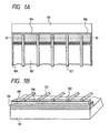
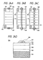
- Figs. 24A to 24D illustrate schematically a conventional photovoltaic element for comparison with the one of the present invention.
- Figs. 24A to 24C illustrate steps of forming a collecting electrode
- Fig. 24D is a cross-sectional view along the line 24D-24D in Fig. 24C.
- the solar cell element 500 of Figs. 24A to 24D is prepared by laminating a lower electrode layer 502 on the surface of a substrate 501, a semiconductor layer 503 thereon, and an upper electrode layer 504 further thereon successively.
- the collecting electrodes 506 is prepared by applying an electroconductive paste on the face of electrode formation by screen printing and heat curing it.
- the electroconductive paste includes various materials.
- polymer pastes comprising a thermosetting resin such as of polyester type, epoxy type, and phenol type, and a fine particulate material such as silver and copper dispersed therein are frequently used.
- a bus bar electrode 507 is provided which further collects the generated power from the above collecting electrode 506 (Fig. 24B). Then crossing points of the bus bar electrode 507 over the collecting electrodes 506 are connected by applying an electroconductive adhesive 508 in spots and curing it in an air drier (Fig. 24C). Thus a leading electrode which takes out the power from the upper electrode 504 is prepared by electrically connecting the collecting electrodes 506 with the bus bar electrode 507. Insulation tapes 509 are applied at the ends of the solar cell element 500 to ensure the electrical separation of the bus bar electrode 507 from the substrate.
- Usual family consumption of electric power is about 3 KW per family.
- the solar cell needs to have a light-receiving area of as large as 30 m 2 by assuming the photovoltaic conversion efficiency of the cell to be 10%.
- Such a large solar cell is required to have a bus bar to collect the generated power, which increases the cell element production steps. The larger the number of the production steps, and the larger the area of the cell, the more would the defects of the element be developed. The defects cause shunting and short circuit to lower the photovoltaic conversion efficiency. If the defect is distant from the electrodes or the bus bar, loss of the current is relatively small because of high resistance to the current flowing into the defective portion. To the contrary, if the defect is beneath the electrode or the bus bar, the loss of the current will be large.
- US-A-4,260,429 discloses a process in which a copper wire is covered with a solid polymer containing electroconductive particles and is attached as the electrode to a solar cell.
- US-A-5,084,107 discloses a process in which a metal wire is connected and fixed by an electroconductive adhesive to an electrode formation surface of a photovoltaic element.
- an electrode is formed by covering an electroconductive wire with an electroconductive particle-containing solid polymer (electroconductive adhesive) with a low ohmic loss even with an electrode length of 10 cm or more.
- the electrodes formed by the methods of the above USPs are insufficient in adhesiveness at the interface between the electroconductive wire or the metal member and the electroconductive particle-containing solid polymer or the electroconductive adhesive, and electrodes are not uniform in the width or diameter.
- the insufficient adhesiveness at the interface between the electroconductive wire or the metal member and the electroconductive adhesive causes initial power loss, increase of series resistance by peeling at the interface in a long-term run resulting in drop of conversion efficiency, and other problems in reliability.
- shunting and low yield may be caused depending on the resistance of the electrode layer formed from the electroconductive adhesive, and migration of ionic substances may be caused by interaction with water, resulting in leakage by humidity in practical use, disadvantageously.
- the coated wires are bonded by heating or pressing, but neither the apparatus nor the method are shown specifically.
- usual method of heat-press bonding causes spreading of the coating polymer to increase shadow loss, and particularly in a large-area photovoltaic element, the pressure applied to the coated wire becomes non-uniform to give non-bonded portions to increase the series resistance, disadvantageously.
- Electric connection is further considered for taking out the generated power of the photovoltaic element.
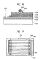
- Fig. 17 is a schematic plan view of a photovoltaic element from the front side (light-receiving side) for comparison.
- the photovoltaic element of Fig. 17 is constituted from an electroconductive substrate for supporting the entire photovoltaic element, a noncrystalline semiconductor layer, an electrode layer, collecting electrodes, and leading-out terminals formed successively on the substrate.
- the electroconductive substrate is made of a metallic material such as stainless steel.
- the semiconductor layer is constituted from a back-face reflection layer, a p-type semiconductor layer, an i-type semiconductor layer, and an n-type semiconductor layer arranged successively from the bottom layer.
- the aforementioned electrode layer is a light-transmissive electroconductive film made of indium oxide or the like, serving both as a reflection-preventing means and as a power-collecting means.
- the light-transmissive electroconductive film is formed by application of an etching-paste containing FeCl 3 , AlCl 3 , or the like by screen printing, and subsequent heating.
- An etched groove 17401 is formed by removing the light-transmissive electroconductive film by etching in a line shape. This partial removal of the light-transmissive electroconductive film is conducted for preventing the influence of the short circuit between the substrate and the light-transmissive electroconductive film on the effective light-receiving area of the photovoltaic element. Such short-circuit may occur in cutting of the outer periphery of the photovoltaic element.
- collecting electrodes 17402 are formed for collecting efficiently the generated power.
- the collecting electrodes 17402 are formed by using a fine metal wire of low resistance such as copper as the core material, applying an electroconductive adhesive on the outer surface of the metal wire for adhesion, drying the adhesive, cutting the wire in a predetermined length, arranging the cut wires, and heat-bonding the wires on the surface of the effective light-receiving area by hot pressing entirely.
- the power collected by the collecting electrode 17402 is transmitted to leading-out terminals 17403 provided on both ends of the element.
- the leading-out terminal 17403 is a foil made of a low-resistance metal such as copper, and has an insulating member 17404 as the lowest layer to insulate the terminal foil from the surface of the photovoltaic element.
- connection between the collecting electrodes 17402 and the leading-out terminals 17403 is conducted by spot-like application of an electroconductive adhesive 17405 to ensure the reliability of the connection.
- This process involves the problems of: necessity of spot-like application step of an electroconductive adhesive, requiring a heat-curing step for curing the electroconductive adhesive, thereby increasing the working steps and taking long time and using a complicated apparatus for conducting these steps; the high cost for the electroconductive adhesive; the protrusion of the spot-wise applied electroconductive adhesive requiring thickness of surface coating material, thus raising the production cost; deterioration of the surface of the terminal material such as copper by oxidation and other causes in heating process of the element prior to the application of the electroconductive adhesive, thus a sufficient low connection resistance not being obtained by the application of the electroconductive adhesive.
- document JP-06-132 551 discloses the formation of an electrode with low cost and little resistance loss and the improvement of the degree of adhesion to an electrode-forming surface by improving the strength of a metal body against pressure in an electrode-bonding process.
- document JP-06-132 551 discloses that a copper wire is fixed by an adhesive applied to a polyethylene film, and a conductive adhesive is attached to the lower part of the copper wire. Then, the copper wire is pressed to an electrode-forming surface of an amorphous silicon solar cell as the wire is fixed to the polyethylene film. The copper wire is heat-treated in the pressed state so that the conductive adhesive is heat-hardened and the copper wire is fixed to the electrode-forming surface.
- Figs. 1A and 1B illustrate schematically the structure of the electrode of Example 1-1.
- Fig. 2 illustrates schematically the photovoltaic element of Example 1-1.
- Fig. 3 illustrates schematically an apparatus for applying an electroconductive adhesive over the entire length of a metal wire employed in Example 1-1.
- Fig. 4 illustrates schematically an apparatus employed in Example 1-1 for fixing the metal wire onto a conductor with an electroconductive adhesive.
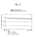
- Fig. 5 is a graph showing deterioration of a photovoltaic element module of Comparative Example.
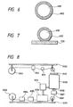
- Fig. 6 is a schematic sectional view showing constitution of metal wire coated with an electroconductive resin.
- Fig. 7 is a schematic sectional view of an electrode fixed on an upper electrode of a photovoltaic element .
- Fig. 8 illustrates schematically an apparatus for coating an metal wire with an electroconductive resin.
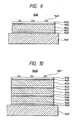
- Fig. 9 illustrates schematically constitution of a photovoltaic element .
- Fig. 10 illustrates schematically constitution of a triple type of photovoltaic element.
- Fig. 11 is a schematic plan view showing constitution of a solar cell.
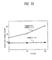
- Fig. 12 is a graph showing change of series resistance by temperature-humidity cycle test.
- Fig. 13 is a graph showing change of series resistance by temperature-humidity cycle test.
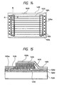
- Fig. 14 illustrates schematically an external appearance of a photovoltaic element of an Example of the present invention.
- Fig. 15 is a schematic sectional view of a part of the photovoltaic element along the line 15-15 in Fig. 14.
- Fig. 16 is a schematic sectional view of a part of the photovoltaic element along the line 16-16 in Fig. 14.
- Fig. 17 illustrates schematically an external appearance of a photovoltaic element of prior art for comparison.
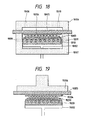
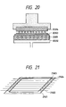
- Fig. 18 illustrates schematically an apparatus suitable for formation of an electrode.
- Fig. 19 illustrates schematically another apparatus suitable for formation of an electrode.
- Fig. 20 illustrates schematically still another apparatus suitable for formation of an electrode.
- Fig. 21 illustrates schematically a process for formation of an electrode.
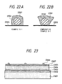
- Figs. 22A and 22B are schematic sectional views of a collecting electrode of a photovoltaic element formed according to the method of descriptive Example 5-1 and the method of prior art, respectively.
- Fig. 23 is a schematic sectional view of a photovoltaic element.
- Figs. 24A to 24D illustrate a photovoltaic module for comparison.
- a photovoltaic device described hereinafter for better understanding the present invention comprises a metal wire arranged on a photovoltaic element for collecting the power generated by the photovoltaic element, the metal wire being fixed with an electroconductive adhesive applied over the entire length of the metal wire.
- the metal wire employed for collecting the generated power is coated preliminarily on the surface with an electroconductive adhesive over the entire length thereof.
- an electroconductive adhesive On curing the electroconductive adhesive on the metal wire arranged on the electrode formation face, a leading-out conductor can be simultaneously fixed by the aforementioned electroconductive adhesive. Consequently, the step of application of an electroconductive adhesive in spots and the step of curing the adhesive may be omitted which are necessary conventionally for connection between the leading-out electrode and the collecting electrodes, thereby shortening significantly the time for working.
- the element production steps are greatly simplified since the steps including the fixation of the collecting electrodes and the leading-out electrodes are completed in the present invention within a time of fixation of the collecting electrodes (printing and curing of an electroconductive paste) in a conventional process shown in comparison.
- the electrode of the photovoltaic element comprises a metal member such as a metal wire or a metal bar treated for rust prevention and coated on the surface thereof with at least one electroconductive resin layer.
- a further photovoltaic device described hereinafter for better understanding the present invention comprises a photovoltaic element comprising at least one pair of a semiconductor junction and a light-transmissive upper electrode formed on a semiconductor layer on the light-receiving face of the semiconductor junction, the above electrode of the photovoltaic element being fixed on the upper electrode.
- the fixation of the electrode of the photovoltaic element is made through the electroconductive resin.
- the metal member is preferably made of copper or a copper alloy.
- the member is preferably protected from rusting by a rust-preventing agent of an imidazole type, a triazole type, or a mercaptan type.
- the electroconductive resin layer has a specific resistance ranging preferably from 0.1 to 100 ⁇ cm.
- the electrode has been found after experiments to obtain satisfactory adhesion and satisfactory electroconductivity of a metal wire or a metal bar with an electroconductive adhesive, and is characterized by the rust-preventing treatment and electroconductive resin coating of the metal wire or the metal bar.
- the excellent properties of the electrode are considered to be obtained by the reasons below. Copper wires, aluminum wires, and the like having low resistance and generally used for electric apparatuses are inexpensive suitable materials for conductors. However, the surface thereof will be oxidized under environmental conditions (corrosive material in the air, and humidity), especially under severe temperature-humidity cycles, deteriorating the adhesiveness and electric contact between the metal and the electroconductive resin layer.
- the methods for oxidation prevention of a metal include organic material coating, chemical treatment, alloy formation, electric protection, metal plating, and so forth. However, a metal surface treatment with a rust-preventing agent protects the metal surface against oxidation without change of the electrical properties of the metal surface without complicated processing steps, and yet gives high adhesiveness between the metal and the electroconductive resin layer.
- the electrode of the photovoltaic element comprises a metal wire or a metal bar being treated with a coupling agent and being coated with at least one electroconductive resin layer on the surface thereof.
- the metal member is preferably made of copper or a copper alloy, and the coupling agent is preferably selected from silane type coupling agents, titanate type coupling agents, and aluminum type coupling agents.
- the electroconductive resin layer has a specific resistance ranging preferably from 0.1 to 100 ⁇ cm.
- the electrode has been found after experiments to obtain satisfactory adhesion and satisfactory electroconductivity of a metal wire or a metal bar with an electroconductive adhesive, and is characterized by the coupling-agent treatment and electroconductive resin coating of the metal wire or the metal bar.
- the excellent properties of the electrode are considered to be obtained by the reasons below. Copper wires, aluminum wires, and the like are inexpensive suitable materials for conductors. Enameled wires are metal wires coated with an insulating paint. However, the metal substance which is inorganic cannot readily be coated with a material containing an organic substance.
- the electrode is a metal substance, which is inorganic, coated with an electroconductive resin layer composed of an organic substance. In such a constitution, uniform coating with high adhesiveness is not readily achievable generally. Therefore, the inorganic metallic substance is treated with a coupling agent, thereby the surface of the metal substance being modified for bonding with an organic substance to give high adhesiveness between the metal surface and the organic substance, especially under severe temperature-humidity cycle conditions, with high reliability of the electrode.
- a still further photovoltaic device described hereinafter for better understanding the present invention comprises a photovoltaic element comprising a semiconductor layer for photoelectric conversion and an electrode for collecting electric power generated by the semiconductor layer, wherein the electrode is a fine metal wire coated with at least one kind of a first electroconductive adhesive by application and drying, and is fixed on the light-receiving face of the photovoltaic element by pressing, hot-pressing, or heating; a terminal member is provided for leading out the electric power collected by the electrode on the face of the photovoltaic element; the electrode is also fixed onto the surface of the terminal member; and the terminal member is preliminarily coated with a second electroconductive adhesive at least on the electrode fixation portion.
- the production process and the production apparatus of the photovoltaic element are simplified, and the materials such as the photovoltaic element and the surface coating material are reduced. Thereby, the production cost is reduced, and reliability of the photovoltaic element is improved for a long term for the initial investment.
- the process for producing the collecting electrode for the photovoltaic element comprises placing, on a photovoltaic element, the collecting electrode being constituted of a metal wire coated with at least one layer of an electroconductive adhesive, and heating the photovoltaic element from the face reverse to the placed collecting electrodes with simultaneous pressure application.
- the temperature of the above heating is preferably in the range of from the softening temperature to a temperature higher by 150°C than that.
- the applied pressure is preferably in the range of from 1 to 10 kg/cm 2 .
- a method of fixing a coated wire on a light-receiving face of the photovoltaic element has been found in which the metal wire is coated with an electroconductive adhesive in a dry state; the coated metal wire is placed on a light-receiving face of the photovoltaic element; the electroconductive adhesive is softened by heating from the face of the element reverse to the light-receiving face with simultaneous application of pressure through a soft resin.
- the temperature of heating the electroconductive adhesive is preferably in the range of from the softening point thereof to a temperature higher than that by 150°C, whereby the spreading of the adhesive is less and low shadow loss and high performance of the photovoltaic element is obtainable.
- the applied pressure is preferably in the range of from 98 kPa to 980 kPa (1 to 10 kgf/cm 2 ), whereby the spreading of the electroconductive adhesive is prevented and the adhesion is stable and uniform with high adhesion strength.
- a descriptive metal wire 107 useful for understanding the present invention which is used for passing electric current, is preferably made of a metallic material having a low volume resistivity to minimize the ohmic loss.
- the metallic material is exemplified by gold, silver, copper, nickel, aluminum, and alloys thereof.
- the cross-section may be circular or square or in other shape, and is selected as desired.
- the thickness of the metal wire is selected to make minimum the sum of the ohmic loss and the shadow loss.
- the metal wire is exemplified by a copper wire for enamel wires having diameter of 25 to 200 ⁇ m to obtain an effective solar cell.
- the conductor 106 for leading-out electrode may be made of gold, silver, copper, lead, nickel, and alloys thereof similarly as the above metal wire, but is not limited thereto, and may be a plated metal such as silver-plated copper, and solder-plated copper.
- the shape is not specially limited, and may be in a form of a wire or a foil.
- the electroconductive adhesive needs to have a specific resistance which is negligible in collecting the power generated by the solar cell, and is appropriate not to cause shunting.
- the specific resistance thereof ranges preferably from 0.1 to 100 ⁇ cm. With the specific resistance of 0.1 ⁇ cm or lower, shunting is liable to occur, while with the specific resistance of 100 ⁇ cm or higher, the ohmic loss is larger.
- the electroconductive adhesive having the above preferred specific resistance is obtained by dispersing electroconductive particles in a high polymer resin.
- the material for the electroconductive particles includes graphite, carbon black, In 2 O 3 , TiO 2 , SnO 2 , ITO, ZnO, and oxide semiconductor materials prepared by adding a suitable dopant to the above materials.
- the electroconductive adhesive is further required to be capable of fixing the metal wire by adhesion to the electrode-forming face of the solar cell and the leading-out conductor.
- the electroconductive adhesive is still further required to be capable of protecting the metal wire against external moisture and to be resistant to migration of metal ions from the metal.
- the resin is suitable which exhibits strong adhesiveness and less moisture permeability.
- the resin therefor includes thermosetting resins such as epoxy resins, urethan resins, butyral resins, fluoroplastic resins, and modified resins thereof; and thermoplastic resins such as acrylic resins and styrene resins.
- the electroconductive adhesive is prepared by mixing the aforementioned electroconductive particulate material and the aforementioned polymer resin in an appropriate ratio.
- the ratio of the electroconductive particulate material to the polymer resin is selected suitably depending on the properties of the respective materials.
- the electroconductive particulate material is employed at a content of from 5% to 95% by volume to obtain a suitable specific resistance and a suitable adhesiveness.
- the mixing is carried out by a usual dispersion method such as a three-roll mill and a paint shaker.
- a dispersing agent or a coupling agent may be added as desired.
- the dispersion may be diluted with a suitable solvent during or after the dispersing operation to adjust the viscosity of the electroconductive adhesive.
- the electroconductive adhesive may be applied suitably by a coating film-forming method for an enamel wire.
- a metal wire coated with an electroconductive adhesive is prepared by diluting the electroconductive adhesive with a solvent to obtain a suitable viscosity; applying the diluted adhesive on the metal wire by means of a roll coater or the like to form a coating film thereon; passing the coated wire through a die to obtain a desired coating film thickness; and drying the adhesive by infrared heating or a like method.
- the metal wire coated with an electroconductive adhesive is bonded to the electrode formation face of the solar cell and the leading-out conductor usually as follows.
- the adhesive is a hot-melt resin type
- the adhesion is practiced by softening the adhesive usually by heating and optionally with application of pressure.
- the adhesive is a thermosetting resin type
- a coating film is formed and dried without causing curing reaction, and is cured by heating at the time of adhesion.
- a descriptive photovoltaic element (Fig. 2) useful for understanding the present invention is preferably useful for amorphous silicon type solar cells which are desired to be flexible. It is also useful for other types of solar cells such as monocrystalline silicon type, and polycrystalline silicon type of solar cells, non-silicon semiconductor solar cells, and Schottky junction type solar cells.
- the substrate 201 in a thin-film solar cell like amorphous silicon type cells, supports mechanically a semiconductor layer and may be used as the electrode. Therefore, the substrate 201 may be electroconductive or electrically insulating, while it is required to have heat resistance to the heating temperature on formation of a semiconductor layer 203.
- the electroconductive material for the substrate includes specifically thin sheets and composites of metals such as Fe, Ni, Cr, Al, Mo, Au, Nb, Ta, V, Ti, Pt, and Pb, and alloys of the metals such as brass, and stainless steel, and the like; carbon sheets; and zinc-plated steel plates.
- the electrical insulating material for the substrate includes films and sheets of synthetic resins such as polyester resins, polyethylene resins, polycarbonate resins, cellulose acetate resins, polypropylene resins, polyvinyl chloride resins, polyvinylidene resins, polystyrene resins, polyamide resins, polyimide resins, and epoxy resins having heat resistance; composite of the above resins with glass fiber, carbon fiber, boron fiber, and metal fiber; the above metal thin plate and the above resin plates covered with surface coating of a metal and/or an insulating material such as SiO 2 , Si 3 N 4 , Al 2 O 3 , and AlN formed by sputtering, vapor deposition, metal plating, or the like method; glass and ceramics; and the like.
- synthetic resins such as polyester resins, polyethylene resins, polycarbonate resins, cellulose acetate resins, polypropylene resins, polyvinyl chloride resins, polyvinylidene resins, polyst
- the lower electrode 202 is the one electrode for leading out the electric power generated by the semiconductor layer, and is required to have a work function to give an ohmic contact with the semiconductor layer.
- the material therefor includes simple metals, alloys, and light-transmissive electroconductive oxide (TCO) such as Al, Ag, Pt, Au, Ni, Ti, Mo, Fe, V, Cr, Cu, stainless steel, brass, nichrome, SnO 2 , In 2 O 3 , ZnO, and ITO.
- TCO light-transmissive electroconductive oxide
- the surface of the lower electrode 202 is desirably smooth. When irregular reflection is desired, the surface may be made rough by texture treatment. In the case where the substrate 201 is electroconductive, the lower electrode 202 is not particularly necessary.
- the lower electrode is prepared, for example, by metal plating, vapor deposition, or sputtering.
- the semiconductor layer 203 may be any known semiconductor used generally for thin film solar cells.
- the semiconductor layer of the descriptive solar cell element useful for understanding the present invention includes pin-junction noncrystalline silicon layers (the noncrystalline layers herein including microcrystalline layers), pn-junction polycrystalline silicon layers, and compound semiconductor layers such as CuInSe 2 /CdS.
- the noncrystalline silicon layer can be prepared by plasma CVD by using starting material gas for thin film formation such as silane, and conductivity-controlling phosphine or diborane gas.
- the pn-junction polycrystalline silicon layer can be formed by thin film formation from molten silicon.
- the CuInSe 2 /CdS semiconductor layer can be formed by electron beam vapor deposition, sputtering, electrodeposition or the like method.
- the upper electrode 204 serves as an electrode to lead out the electromotive force generated in the semiconductor layer, and is counter to the lower electrode 202.
- the upper electrode 204 is indispensable for the semiconductor having a high sheet resistance like amorphous silicon, but is not indispensable for a crystal type of solar cell having a low sheet resistance.
- the upper electrode 204 needs to be transmissive at least to the light to be absorbed by the semiconductor, and is sometimes called transparent electrode.
- the upper electrode 204 has preferably light transmittance of 85% or higher for effective absorption of light from the sun or a white fluorescent lamp, and sheet resistance of not higher than 100 ⁇ /cm 2 to allow the generated electric current to flow in a lateral direction of the semiconductor layer.
- the material having such properties includes metal oxides such as SnO 2 , In 2 O 3 , ZnO, CdO, CdSnO 4 , and ITO (In 2 O 3 +SnO 2 ).
- Examples 2-1 to 2-8, and Examples 3-1 to 3-8 are similar to Examples 1-1 to 1-3.
- the material for the metal member includes electroconductive materials such as copper, copper alloys, and gold: copper and copper alloys are suitable used because of inexpensiveness.
- the cross-section may be selected as desired, and may be circular or rectangular.
- metal wires such as a copper wire having diameter ranging from 25 ⁇ m to 1 mm for enamel wires as defined in JIS C3202 are suitably used. Such metal wires are worked by a wire drawing machine into a desired diameter. The metal wire having passed through the metal drawing machine is rigid, and may be annealed to obtain the desired stretchability and flexibility.
- the diameter of the metal wire is selected to minimize the sum of the surface ohmic shadow loss of the solar cell and the ohmic loss, and is preferably in the range of from 25 to 300 ⁇ m.
- the wire pitch is optimized to be narrow for a small wire diameter and to be wide for a large wire diameter to maximize the efficiency.
- the rust-preventing agent employed in the descriptive photovoltaic elements includes imidazole type compounds, triazole type compounds, and mercaptan type compounds.
- This rust-preventing agent differs from generally used rust-preventing paints and rust-preventing oil which form a resin coating film or an oil film to protect metal surface from the outside, but forms a chemical conversion coating on contacting with the surface of the copper or the copper alloy.
- the formed chemical conversion coating is composed of a chelate compound, which retards oxidation of the surface of the copper, and improves the adhesiveness without changing the electrical properties of the treated surface.
- the rust-preventing agent may be employed as a mixture with an acid, water, or an organic solvent. Two or more kinds of rust-preventing agents may be combinedly used.
- the formed chemical conversion coating is a tough film, exhibiting a rust-prevention effect for a long term.
- the electroconductive resin layer formed in contact with the metal wire performs functions of protecting the metal from moisture, resisting migration of metal ions, fixing the metal wire to the solar cell, and collecting the generated electric power.
- the electroconductive resin layer is formed by mixing and dispersing a high polymer resin and a fine particulate electroconductive material to form an electroconductive paint, applying the paint on the metal wire, and drying or heat-curing the paint.
- the polymer resin may be thermosetting or thermoplastic, and is preferably less moisture-permeable.
- the polymer resin includes epoxy resins, urethane resins, butyral resins, phenol resins, melamine resins, alkyd resins, polyester resins, polyimide resins, and fluoroplastic resins.
- a curing agent may be added to the polymer resin for curing the electroconductive resin layer.
- the coupling agent preferably employed includes silane type coupling agents, titanate type coupling agents, and aluminum type coupling agents.
- the coupling agent has a hydrophilic moiety which interacts with inorganic substances and an organic functional moiety which interacts with organic substances.
- the coupling agent is used mainly for controlling the interface between the different substances, and differs from usual surfactants in that the function is based on formation of covalent bonding.
- the coupling agent serves as intermediation between an inorganic substance (metal) and an organic substance (high polymer resin in the electroconductive resin) to bond them strongly.
- the silane type coupling agent is linked by covalent bonding both to the inorganic substance and to the organic substance.
- the titanate type coupling agent and the aluminum type coupling agent do not form a covalent bond with the organic substance.
- the bonding strength to the organic substance can be increased.
- the coupling agent is reacted with the metal surface in an optimum amount, and the amount of the coupling agent is usually adjusted by diluting the coupling agent with a solvent.
- the solvent includes methanol, ethanol, isopropyl alcohol, toluene, benzene, acetone, methylcellosolve, tetrahydrofuran, water, and the like.
- the solvent is used which is compatible with the coupling agent. Since at a higher concentration, the coupling agent comes to be inactivated, the coupling agent is used usually at a lower concentration, preferably in the range of from 0.1% to 5.0%.
- the suitability of the hydrolyzable group of the coupling agent of the silane type, the titanate type, or the aluminum type to the inorganic substance needs to be considered.
- the organic functional group of the coupling agent includes groups of amino, epoxy, carboxyl, and phosphite, and the suitability of these groups to the organic compound needs to be considered.
- the treatment of the metal wire with the coupling agent may be conducted by spraying; dipping, roll-coating as conducted for enamel wire coating, and the like method.
- a simple method preferably employed is coating by passing the metal wire through a felt or the like containing a coupling agent.
- the surface of the metal wire is preferably cleaned preliminarily to remove any oily matter or staining by treatment with a cleaning solvent such as acetone, methyl ethyl ketone, and isopropyl alcohol. These solvents are preferred because of the high volatility not to remain on the metal surface.
- the metal wire is dried under prescribed conditions to evaporate off the solvent and simultaneously to accelerate the reaction of the coupling agent with the metal. The drying conditions are selected depending on the kind of the coupling agent and the kind of the metal.
- the electroconductive resin layer formed in contact with the metal wire performs functions of protecting the metal from moisture, resisting migration of metal ions, fixing the metal wire to the solar cell, and collecting the generated electric power.
- the electroconductive resin layer is formed by mixing and dispersing a high polymer resin and a fine particulate electroconductive matter to form an electroconductive paint, applying the paint on the metal wire, and drying or heat-curing the paint.
- the polymer resin may be thermosetting or thermoplastic, and is preferably less moisture-permeable.
- the polymer resin includes epoxy resins, urethane resins, butyral resins, phenol resins, melamine resins, alkyd resins, polyester resins, polyimide resins, and fluoroplastic resins.
- a curing agent may be added to the polymer resin for curing the electroconductive resin layer.
- the adhesion of the electroconductive resin with the metal is improved by selecting a suitable coupling agent.
- the electroconductive adhesive is required to have a specific resistance which is negligible in collecting the electric power generated by the solar cell and is appropriate not to cause shunting.
- the specific resistance thereof ranges preferably from 0.1 to 100 ⁇ cm.
- the electroconductive adhesive having the above preferred specific resistance is obtained by dispersing electroconductive particles in a high polymer resin.
- the material for the electroconductive particles includes carbon black, graphite, In 2 O 3 , TiO 2 , SnO 2 , ITO, ZnO, and oxide semiconductor materials prepared by adding a suitable dopant to the above materials.
- the electroconductive particles are required to have a diameter smaller than the thickness of the electroconductive coating layer to be formed. However, with an excessively small diameter, the resistance at the contact point of the particles is large not to give desired low specific resistance. Therefore, the particle diameter of the electroconductive particles is preferably in the range of from 0.02 to 15 ⁇ m.
- the electroconductive particulate material and the polymer resin are mixed in an appropriate ratio. With a higher ratio of the electroconductive particulate material, although the specific resistance is lower, the stability of the coating film is lower because of the less amount of the resin. Accordingly, the ratio of the electroconductive particulate material to the polymer resin is selected suitably depending on the properties of the respective materials. Specifically the electroconductive particulate material is employed at a content of from 5% to 95% by volume to obtain a suitable specific resistance.
- the two materials are mixed by a usual dispersion method such as a three-roll mill and a paint shaker. The dispersion may be diluted with a suitable solvent during or after the dispersing operation to adjust the viscosity of the electroconductive adhesive.
- the thickness of the electroconductive resin layer is selected depending on the diameter of the metal wire and the intended properties.
- the thickness is preferably in the range of from 1 to 30 ⁇ m in order to avoid pinhole formation, to obtain the sufficient function of a barrier layer, and to avoid remarkable shadow loss.
- the electroconductive resin layer is preferably made of a hot-melt type resin to be bonded to the solar cell by softening by heating. An appropriate pressure may be applied on the bonding.
- the electroconductive layer is thermoplastic, the layer becomes softened by heating.
- the electroconductive layer is thermosetting, the solvent may be removed by drying on coating the metal wire without curing, and the electroconductive layer may be cured at the time of bonding.
- Fig. 6 shows a cross-section of a metal wire electrode coated with an electroconductive resin.
- Fig. 7 shows a cross-section of a part of a photovoltaic element in which an electrode is fixed on an upper electrode by an electroconductive resin.
- the metal wire 6101 is coated with an electroconductive resin layer 6102.
- the numeral 7201 indicates a main body of a photovoltaic element having a laminated upper electrode.
- the electroconductive resin layer 6102 is preferably formed on the wire 6101 concentrically therewith.
- the electroconductive resin may be applied by dipping. However, it is suitably applied by a usual enamel wire coating method. Specifically, the electroconductive paint is diluted to obtain an appropriate viscosity; the diluted paint is applied onto the metal wire by a roll coater or the like; the metal wire is allowed to pass through a die to obtain a desired film thickness; and then the wire is heated by infrared heating or a like method to dry and cure the paint.
- Fig. 8 illustrates schematically a specific example of an apparatus for coating a metal wire with an electroconductive resin.
- the wire may be delivered either vertically or horizontally.
- the numeral 8301 indicates a metal wire; 8302 a delivery reel; 8303 stretching devices; 8304 a cleaning vessel; 8305 a vessel for rust-prevention treatment and/or coupling agent treatment; 8306 a drying furnace; 8307 a coater; 8308 a die; 8309 a curing-drying furnace; 8310 a thickness tester; 8311 a tension controller; 8312 a regular wind-up driving device; 8313 a wind-up reel; and 8314 a temperature controller.
- the delivery reel 8302 is a bobbin having uncoated metal wire wound thereon. Tension is applied to the metal wire throughout the coating apparatus by the stretching devices 8303 to keep the wire tight-stretched.
- the cleaning vessel 8304 is an optionally employed vessel filled with a solvent such as acetone, methyl ethyl ketone, and isopropyl alcohol, serving to clean the surface of the metal wire 8301.
- the vessel 8305 contains a rust-preventing agent and/or a coupling agent and treat the metal wire 8301 for rust prevention and/or coupling.
- the drying furnace 8306 is an air drier or an infrared drier for drying the rust-preventing agent and/or the coupling agent applied on the metal wire.
- the coater 8307 is a device for applying the electroconductive paint onto the metal wire 8301.
- the coater stores the electroconductive paint, and may further be provided with a solvent-supplying mechanism for viscosity adjustment, a temperature-controlling mechanism, an electroconductive paint-replenishing mechanism, filtering mechanism, and the like.
- the die 8308 controls the thickness of the applied electroconductive paint.
- a commercial die for enamel coating is suitably used as the die 8308. If desired, felt may be employed.
- the curing-drying furnace 8309 removes the solvent from the electroconductive paint to dry it, or cures the paint, and may be an air drier or an infrared dryer.
- the thickness tester 8310 measures and controls the thickness of the applied electroconductive paint, and a commercial outer-diameter tester is suitable for it.
- the wire delivery rate, or paint viscosity may be controlled by feeding back the film thickness measured by the thickness tester 8310.
- the tension controller 8311 applies tension constantly to the metal wire to cause neither loosening nor yielding of the wire.
- the regular wind-up driving device 8312 winds up the metal wire with a controlled spacing between the wire to the wind-up reel 8313.
- the wind-up reel 8313 is rotated to keep the prescribed delivery rate by a motor not shown in the drawing.
- the temperature controller 8314 controls the temperatures of the drying furnace 8306 and the curing-drying furnace 8309 as prescribed by a conventional control method such as voltage control, on-off control, and PID control.
- the apparatus in Fig. 8 is of a vertical type.
- the delivery direction of the metal wire may be either vertical or horizontal.
- the apparatus of Fig. 8 conducts single wire coating, but two or more wires may be simultaneously treated for coating.
- the electroconductive resin layer may be constituted of a plurality of layers, and the functions of power collection, shunting prevention, migration prevention, electrode fixation, etc. may be assigned to the respective layers.
- Two or more layer coating may be conducted with bobbin wind-up for every coating step, or with successive formation of a plurality of coating layers and final bobbin wind-up.
- FIG. 9401 is a supporting substrate; 9402 a lower electrode; 9403, 9404, and 9405 respectively a semiconductor layer; 9406 an upper electrode; and 9407 an electrode (grid electrode).
- the grid electrode 9407 is constituted of a metal wire 6101 and an electroconductive resin layer 6102.
- the electroconductive resin layer 6102 needs to have a resistance which does not impair the efficiency of the photovoltaic element but is sufficiently high to prevent shunting. Thereby, the resin layer is not a resistance to the electric current generated by the solar cell but serves as a resistance to defects to prevent significant leakage.
- the specific resistance of the electroconductive resin layer 6102 is selected in consideration of the design of the grid, the current intensity at the working point of the photovoltaic element, and is preferably in the range of from 0.1 to 100 ⁇ cm. Within this range, the resistance is sufficient to offset possible shunting and is negligible to the electric current generated by the photovoltaic element.
- the grid electrode 9407 is placed on the light-receiving face side of the photovoltaic element 9400, preferably in parallel at an appropriate spacing.
- the grid is particularly suitable for a large-area solar cell. For example, to prepare a solar cell of 30 cm square, grid electrodes of 30 cm long are placed in parallel at a prescribed spacing.
- the grid electrode which has constitution of minimizing electric leakage caused by shunting, is useful not only for amorphous silicon type solar cells but also for photovoltaic elements having semiconductor junction such as pn junction, pin junction, and Schottky junction. The same constitution is naturally applicable also to solar cells employing a semiconductor of monocrystalline type, polycrystalline type, non-silicon type, or Schottky junction type.
- Fig. 9 illustrates schematically an amorphous silicon type solar cell having a single cell structure, and receiving light on the face reverse to the substrate.
- Fig. 10 illustrates schematically amorphous silicon type solar cell of triple construction.
- Fig. 11 is a plan view of the solar cell of Fig. 9 and Fig. 10 viewed from light-introducing face side, having grid electrodes of about 30 cm long.
- the constitution is naturally applicable also to amorphous silicon type solar cells, monocrystalline type and thin film polycrystalline type solar cells formed on a light-transmissive insulating substrate.
- the supporting substrate 9401 is a member for supporting mechanically the semiconductor layers 9403, 9404, 9405 like thin films of amouphous silicon of a solar cell, and in some cases, it is used as an electrode.
- the substrate 9401 needs to be heat-resistant at heating temperature for forming the films of the semiconductor layers 9403, 9404, 9405, but may be either electroconductive or insulating.
- the electroconductive material includes specifically thin sheets and composites of metals such as Fe, Ni, Cr, Al, Mo, Au, Nb, Ta, V, Ti, Pt, Pb, and Ti; alloys of the metals such as brass, stainless steel; carbon sheets; galvanized sheet iron; and the like.
- the electrically insulating material includes specifically films or sheets of heat-resistant synthetic resins such as polyesters, polyethylenes, polycarbonates, cellulose acetates, polypropylenes, polyvinyl chlorides, polyvinylidene chlorides, polystyrenes, polyamides, polyimides, and epoxy resins; composites of the above resins with fiber such as glass fiber, carbon fiber, boron fiber, and metal fiber; the above resin sheets and metal sheets surface-coated with different kinds of metal thin film and/or insulating thin film such as SiO 2 , Si 3 N 4 , Al 2 O 3 , and AlN by sputtering, vapor deposition, metal plating, or the like; and glass and ceramics.
- synthetic resins such as polyesters, polyethylenes, polycarbonates, cellulose acetates, polypropylenes, polyvinyl chlorides, polyvinylidene chlorides, polystyrenes, polyamides, polyimides, and epoxy resins
- the lower electrode 9402 is the one of the electrodes, and leads out the electric power generated in the semiconductor layers 9403, 9404, 9405, having a work function to give ohmic contact with the semiconductor layer 9403.
- the material therefor includes simple metals, alloys, and light-transmissive electroconductive oxide (TCO) such as Al, Ag, Pt, Au, Ni, Ti, Mo, W, Fe, V, Cr, Cu, stainless steel, brass, nichrome, SnO 2 , In 2 O 3 , and ITO.
- TCO light-transmissive electroconductive oxide
- the surface of the lower electrode 9402 is desirably smooth. When irregular reflection is desired, the surface may be made rough by texture treatment. In the case where the substrate 9401 is electroconductive, the lower electrode 9402 is not particularly necessary.
- the lower electrode is prepared, for example, by metal plating, vapor deposition, or sputtering.
- the upper electrode may be prepared by resistance-heating vapor deposition, electron beam heating vapor deposition, sputtering, spraying, or the like method.
- the semiconductor layer employed for the solar cell is formed from amorphous silicon, polycrystalline silicon, monocrystalline silicon, or the like.
- the semiconductor material constituting the i-layer 9404 includes Group IV metal type and Group IV metal alloy type amorphous semiconductors such as a-Si:H, a-Si:F, a-Si:H:F, a-SiGe:H, a-SiGe:F, a-SiGe:H:F, a-SiC:H, a-SiC:F, and a-SiC:H:F.
- the semiconductor material for constituting the p-layer 9405 or the n-layer 9403 is obtained by doping a valence electron controlling agent into the aforementioned semiconductor material for the i-layer 9404.
- the valence electron controlling agent for the p-type semiconductor includes compound having Group III element of Periodic Table, such as B, Al, Ga, and In.
- the valence electron controlling agent for the n-type semiconductor includes compound having Group V element of Periodic Table, such as P, N, As, and Sb.
- the amorphous silicon semiconductor layer is formed by a conventionally known method including vapor deposition, sputtering, RF plasma CVD, microwave plasma CVD, ECR, thermal CVD, and LPCVD.
- RF plasma CVD is suitably applicable in which the starting material gas decomposed by RF plasma is deposited on a substrate.
- the RF plasma CVD has disadvantages of low decomposition efficiency of the starting material gas of about 10% and the low deposition rate of 0,1 to 1 ⁇ m/s (1 to 10 ⁇ /sec).
- Microwave plasma CVD which is improvement of the RF plasma is also applicable without the above disadvantage.
- the reaction apparatus for the film formation may be of batch types or of continuous types and may be selected from known conventional apparatuses.
- the solar cell may be a tandem cell or a triple cell in which two of more semiconductor junction are laminated for improvement of spectral sensitivity and voltage.
- the upper electrode 9406 serves as an electrode to lead out the electromotive force generated in the semiconductor layer 9403, 9404, 9405, and is counter to the lower electrode 9402.
- the upper electrode 9406 is necessary for the semiconductor having a high sheet resistance like amorphous silicon, but is not indispensable for a crystal type of solar cell having a low sheet resistance.
- the upper electrode 9406 needs to be transmissive at least to the light to be absorbed by the semiconductor, and is sometimes called transparent electrode.
- the upper electrode 9406 has preferably light transmittance of 85% or higher for effective absorption of light from the sun or a white fluorescent lamp, and sheet resistance of not higher than 100 ⁇ /cm 2 to allow the generated electric current to flow in a lateral direction of the semiconductor layer.
- the material having such properties includes metal oxides such as SnO 2 , In 2 O 3 , ZnO, CdO, CdSnO 4 , and ITO (In 2 O 3 +SnO 2 ).
- the tab 11601 is a power-collecting part, which may be made of a metal such as Cu, Ag, and Pt, or an alloy thereof (see Fig. 11).
- the tab is preferably in a shape of a sheet, a tape, or a foil, and is bonded with an adhesive or the like.
- the solar cell prepared as above is encapsulated in a known method to prepare a module in order to obtain weatherability and to keep mechanical strength in outdoor use.
- EVA ethylene-vinyl acetate copolymer
- a fluoroplastic resin is laminated as the surface protection layer to improve moisture resistance and to protect mechanically.
- the fluoroplastic resin includes tetrafluoroethylene polymer (TFE, Teflon produced by DuPont), tetrafluoroethylene-ethylene copolymer (ETFE, Tefzel produced by DuPont), polyvinyl fluoride (Tedler produced by DuPont), and polychlorofluoroethylene (CTFE, Neoflon produced by Daikin Kogyo).
- TFE Tetrafluoroethylene polymer
- ETFE Tefzel produced by DuPont
- PETFE Tefzel produced by DuPont
- PETFE tetrafluoroethylene-ethylene copolymer
- CTFE polychlorofluoroethylene
- Neoflon produced by Daikin Kogyo a known ultraviolet absorber may be added to improve weatherability.
- the encapsulation is preferably conducted by heating and pressing the resin film and the solar cell substrate in a vacuum by means of a known apparatus such as a vacuum laminator.
- photovoltaic material including amorphous semiconductors, crystalline semiconductors, and compound semiconductors may be used without restriction.
- the terminal member is preferably prepared from a metal having a low volume resistivity such as copper, silver, aluminum, and nickel. Metals containing copper component are preferred, because of low resistance and inexpensiveness of the terminal member and possibility of minimizing transmission loss to obtain larger power per area.
- An electroconductive adhesive containing carbon, a low-resistivity metal, a metal oxide, or the like is useful as the first electroconductive adhesive.
- High polymer materials containing powdery carbon are particularly preferred, because they are capable of forming ohmic connection with the photovoltaic element to realize low contact resistance with low resistance loss.
- An electroconductive adhesive containing carbon, a low-resistivity metal, a metal oxide, or the like is useful as the second electroconductive adhesive.
- High polymer resins containing powdery material mainly composed of silver or containing a powdery metal or alloy coated with silver are preferred, because they enable connection of low resistance with less liability of oxidative and other deterioration.
- the terminal member is prepared from a copper-containing metal and the first electroconductive adhesive is a carbon-containing high polymer resin, the copper surface is liable to undergo electrochemical oxidative deterioration (anodic oxidation) at the contacting interface.
- the second electroconductive adhesive which is composed of a high polymer resin containing a powdery material mainly composed of silver or containing a powdery metal or alloy coated with silver.
- the metal wire is prepared from a sufficiently electroconductive material such as copper, silver, and gold.
- the cross-section of the metal wire may be selected as desired, and may be circular or rectangular.
- metal wires such as a copper wire having diameter ranging from 25 ⁇ m to 1 mm for enamel wires as defined in JIS C3202 are suitably used.
- Such metal wires are worked by a wire drawing machine into a desired diameter.
- the metal wire having passed through the metal drawing machine is rigid, and may be annealed to be flexible to obtain the desired stretchability and flexibility.
- the diameter of the metal wire is selected to minimize the sum of the surface ohmic shadow loss of the solar cell and the ohmic loss, and is preferably in the range of from 25 to 200 ⁇ m.
- the wire pitch is optimized to be narrow for a small wire diameter and to be wide for a large wire diameter to maximize the efficiency.
- the electroconductive adhesive may be applied by a usual enamel wire coating method. Specifically, the electroconductive paint is diluted to obtain an appropriate viscosity; the diluted paint is applied onto the metal wire by a roll coater or the like; the metal wire is allowed to pass through a die to obtain a desired film thickness; and then the wire is heated by infrared heating or a like method to dry and cure the paint.
- the delivery direction of the metal wire may be either vertical or horizontal.
- Two or more electroconductive adhesive layer coatings may be conducted with bobbin wind-up for every coating step, or with successive formation of a plurality of coating layers and final bobbin wind-up.
- the metal wire coated with the electroconductive adhesive is stored in the wound-up state and is unwounded on formation of the grid of the solar cell.
- a suitable solar cell for the above-described electrode preferably comprises a semiconductor layer for power generation, a light-transmissive electroconductive layer provided on the light-receiving face of the semiconductor layer, a first electrode as described above provided on the light-transmissive electroconductive layer, and a second electrode provided on the face of the semiconductor layer reverse to the light-receiving face.
- the aforementioned semiconductor layer has a structure of semiconductor junction such as pn-junction, pin-junction, and Sehottky junction.
- the material therefor includes IV Group semiconductors such as crystalline silicon, polycrystalline silicon, and amorphous silicon; II-VI Group semiconductors such as CdS, and CdTe; and III-V Group semiconductors such as GaAs.
- the first electrode is placed on the light-receiving face of the semiconductor layer, preferably in parallel at an appropriate spacing.
- the electrode is particularly suitable for a large-area solar cell. For example, in a solar cell of 30 cm square, grid electrodes of 30 cm long are placed in parallel at a prescribed spacing.
- Figs. 18 to 20 show apparatuses suitable for preparing a collecting electrode.
- Fig. 18 is a schematic sectional view of a vacuum heating apparatus.
- the numeral 18101 indicates a heating plate; 18102 a heater; 18103 a photovoltaic element; 18104 a resin film; 18105 a resin sheet; 18106 an upper chamber; 18107 a lower chamber; and 18108 and 18109 respectively an exhaust vent.
- the heating plate 18101 heats the photovoltaic element 18103 and simultaneously conducts adhesion by pressurization with the resin sheet 18105.
- the heater is controlled to keep the surface temperature uniform.
- the photovoltaic element 18103 is placed on the heating plate 18101 with the collecting electrode side directed upward.
- the resin film 18104 is employed as desired to prevent adhesion of the electroconductive adhesive to the resin sheet 18105, and to prevent transfer of oil or other component released from the resin sheet to the photovoltaic element.
- the material of the resin film is preferably a film of a known high polymer such as PFA and ETFE, having a thickness of about 100 ⁇ m thick.
- the resin sheet 18105 is heat resistant and durable, and is employed for maintaining vacuum and applying the pressure uniformly.
- the material thereof includes elastic materials such as silicon rubber, fluororubber, and neoprene rubber.
- the thickness and the elasticity of the above sheet is designed as desired, and preferably in the range of from 1 to 5 mm. With the thickness of less than 1 mm, compression strain is too small to apply pressure uniformly to the coated wire. With the thickness of more than 5 mm, the compression strain is too large to apply sufficient pressure to the coated wire, resulting in poor adhesion of the coated wire.
- the exhaust vents 18108, 18109 are connected to a vacuum pump not shown in the drawing, and the upper chamber 18106 and the lower chamber 18107 are evacuated. If desired, the lower chamber 18107 only may be evacuated and the upper chamber 18106 may be kept at atmospheric pressure.
- Fig. 19 shows a heating apparatus employing no vacuum.
- a pressing plate 19206 applies pressure uniformly to a photovoltaic element 19203.
- a cooling means may be provided if desired.
- Fig. 20 shows a heating apparatus suitable for treating a long photovoltaic element.
- the numeral 20304 indicates a roller.
- the roller 20304 may be formed by covering a material similar to the resin sheet 19205 with the resin film 19204 in Fig. 19.
- This apparatus is capable of applying pressure locally, and uniformly even if the photovoltaic element has a large area.
- the applied pressure ranges preferably from 98kPa to 980kPa (1 to 10 kgf/cm 2 ).
- the thermally softened electroconductive adhesive is not sufficiently squeezed to result in a smaller area of adhesion with the photovoltaic element and to give a higher series resistance, while with a higher pressure, the thermally softened photovoltaic element is squeezed and spread widely to result in a high shadow loss.
- the above processes for producing the collecting electrode are characterized by softening of the electroconductive adhesive coating of the coated wire by heating of the face on which electrode is to be provided.
- the face for forming the electrode may be directed upwards or downward provided that the electroconductive adhesive of the coated wire can be softened by the heat of the face of electrode formation.
- the second electrode of the solar cell is provided on the back face of the semiconductor layer, and is formed from a metal by screen printing, vapor deposition, or the like method.
- the metal is selected from those which are capable of giving sufficient ohmic properties with the semiconductor. If the semiconductor layer is a thin film of amorphous silicon or the like, a supporting substrate is employed which may be insulating or electroconductive.
- Fig. 23 is a schematic sectional view of an embodiment of such a solar cell.
- the numeral 23601 indicates a supporting substrate; 23602 a back side electrode, 23603, 23604, and 23605 respectively a semiconductor layer; 23606 a grid; and 23607 a light-transmissive electrode.
- FIGs. 1A and 1B illustrate the electrode structure schematically.
- Fig. 1A is a schematic top view of the face having collecting electrode formed thereon.
- Fig. 1B is a perspective view of the cross-section taken along the line 1B-1B in Fig. 1A.
- the photovoltaic element 101 in Figs. 1A and 1B has a structure constituted of the multiple layered film shown in Table 1.
- a pattern 103 was screen-printed with a paste containing an ITO etching material (e.g., FeCl 3 ).
- the printed portion was washed with pure water to remove a portion of the ITO layer to form an etched groove 103 to ensure electric separation between the surface electrode and the back face electrode.
- a polyimide insulation tape 104 of 130 ⁇ m thick was stuck on the portion where the power-generation region 102 is adjacent to the exposed face of the substrate.
- a copper foil 106 of 100 ⁇ m thick (hard copper foil, produced by Fukuda Kinzoku K.K.) was fixed as a conductor for leading out the surface electrode by use of a heat-resistant double-face adhesive tape 105 (VHB 9460, produced by Sumitomo 3M K.K.).
- the wires 107 shown in Figs. 1A and 1B were prepared by applying and drying an electroconductive adhesive preliminarily on a copper wire of 100 ⁇ m diameter.
- the electroconductive adhesive was composed of an acrylic resin and carbon black of particle diameter of 3 to 5 ⁇ m as the pigment dispersed therein.
- the process of applying the electroconductive adhesive on the copper wire is described by reference to Fig. 3.
- the copper wire 301 was delivered from the reel 302, and after passing through a container 303 storing the electroconductive adhesive, a die 304, and an IR furnace 305, was wound up by a reel 306.
- the container 303 contained 200 cc of the electroconductive adhesive.
- the reel was controlled to wind up the wire at a rate of 1 m/min.
- the copper wire 301 was passed through the container 303, coated with the electroconductive adhesive in a thickness of 40 to 50 ⁇ m by the die 304, dried in the IR furnace of 1 m long at the inner temperature of 120°C, and then wound up by the upper reel 306.
- the electric power generated in the power generation region 102 of amorphous silicon was collected by the copper wire coated with the electroconductive adhesive, and was lead out by the hard copper foil fixed to the copper wire. The power was lead out through the back face reflecting ZnO layer as the back face electrode from the stainless substrate.
- Fig. 4 illustrates an apparatus employed for preparing the electrode structure shown in Fig. 1.
- This apparatus fixed the metal wire to the conductor by hot pressing.
- the pressing plate 401 was driven vertically by air cylinder, and has a heating means therein.
- the pressing face of the pressing plate was covered with a heat-conductive cushioning material 402.
- a rest 403 for placing the substrate had a heater therein to heat the substrate.
- the heat-conductive cushioning material employed herein was a laminate of a fluororubber and an aramid nonwoven (Type TB, produced by Yamauchi K.K.).
- the substrate of the photovoltaic element which had the insulating tape, the heat resistance double adhesive tape, and the conductor formed thereon was placed on the rest 403 heated at 200°C of the pressing apparatus. Then the copper wires were arranged which had been coated entirely with the hot-melt type electroconductive adhesive. Then it was hot-pressed with the pressing face lined with a cushioning material 402 and heated at 200°C at a pressure of 196kPa (2 kgf/cm 2 ) to fix the copper wire to the hard copper foil.
- This processing step took 2 seconds for substrate setting, 5 seconds for heating the substrate, 3 seconds for arranging the wire, 3 seconds for hot pressing, and 2 seconds for taking-out. Therefore, this step took only about 15 seconds.
- Table 2 shows the evaluation results of the photovoltaic device A which had a collecting electrode connected with a conductor after the paste printing, the photovoltaic device B which had a collecting electrode of the above described construction. The results were obtained respectively with a photovoltaic element of 30cm ⁇ 30cm having respectively the electrode formed as above.
- Photovoltaic device A B C D Comparative Ex. Ex.1-1 Ex.1-2 Ex.1-3 Efficiency ⁇ (%) 7.78 7.82 7.85 7.72 Series resistance Rs ( ⁇ cm 2 ) 30.3 24.6 27.6 27.9 Shunt resistance Rsh (k ⁇ cm 2 ) 80.5 102.1 76.4 92.2
- the photovoltaic element B of this example have the copper wire connected to the copper foil only by hot pressing.
- the photovoltaic device B of this example had Rs of 24.6 ⁇ cm 2
- the photovoltaic element A of a conventional type had Rs of 30.3 ⁇ cm 2 . Since the lower series resistance is preferred, the photovoltaic device having the collecting electrode of the above described construction is considered to have no problem on electroconductivity.
- the photovoltaic device according to the present descriptive Example exhibited a conversion efficiency of 7.82% satisfactorily.
- thermovoltaic device B exhibited a deterioration rate of less than 5%, showing satisfactory long-term reliability.
- this electrode structure gives high initial performances and long-term reliability by a simple production process.
- a photovoltaic element electrode was prepared in the same manner as in Example 1-1 except the four points below:
- the collecting electrodes were fixed to the conductor by hot pressing through the steps of substrate setting in 2 seconds, wire arrangement in 3 seconds, substrate heating for 5 seconds, hot pressing for 10 seconds, taking-out for 2 seconds, and postcuring by an IR heater for 5 seconds. Through these steps, the aluminum wire was fixed to the silver foil.
- the photovoltaic device C having the collecting electrode of the present invention had a series resistance Rs of 27.6 ⁇ cm 2 , and exhibited a conversion efficiency of 7.85% as shown in Table 2. It was confirmed that, even if the members 104 or 107 in Figs. 1A and 1B is changed, the electrode structure can be produced by simple steps by additionally providing a postcuring steps, giving a high initial electrical performances. Further, the ones having a collecting electrode fixed by soldering or paste spot application were subjected to temperature-humidity cycle tests, and the photovoltaic device C exhibited deterioration of less than 5%, showing sufficient long-term reliability.
- a photovoltaic element electrode was prepared in the same manner as in Example 1-1 except the four points below:
- the wire was delivered at a delivery rate of 0.5 m/min, and the temperature of the IR furnace was set at 145°C.
- the collecting electrodes were fixed to the conductor by hot pressing through the steps of substrate setting in 2 seconds, wire arrangement in 3 seconds, substrate heating for 5 seconds, hot pressing for 20 seconds, and taking-out in 2 seconds. Through these steps, the silver wire was fixed to the tin-plated aluminum foil.
- the photovoltaic device D having the collecting electrode of the present example had a series resistance Rs of 27.9 ⁇ cm 2 , and exhibited a conversion efficiency of 7.72% as shown in Table 2. It was confirmed that, even if the members 104 or 107 in Figs. 1A and 1B is changed, the electrode structure can be produced from a different material by selecting the wire delivery rate and the IR furnace temperature, giving a high initial electrical performances. Further, the ones having a collecting electrode fixed by soldering or paste spot application were subjected to temperature-humidity cycle tests, and the photovoltaic device D of the present example exhibited deterioration of less than 5%, showing sufficient long-term reliability.
- the present Example enables simultaneous fixation of a metal wire electrode by curing and a leading-out conductor by the aforementioned electroconductive adhesive, thereby enabling wide selection of the members 104 and 107, and the thermosetting electroconductive adhesive with sufficient electrical properties and long-term reliability at low production cost.
- the steps of application and curing of an electroconductive adhesive which are necessary in conventional process, for connection of the collecting electrode and leading-out electrode are omitted and the working process is simplified. Furthermore, on arrangement and curing the metal wire on the electrode formation face, the leading-out conductor can be simultaneously fixed with the aforementioned electroconductive adhesive, whereby the mass production line can be constructed simply and made flexible with low production cost.
- the collecting electrode was treated for rust prevention to maintain the solar cell performance even in severe environmental conditions.
- the coating of the metal with an electroconductive resin was conducted by use of the apparatus shown in Fig. 8.
- a copper wire 8301 of 100 ⁇ m diameter was stretched by passing it from a reel 8302 through a stretching device 8303.
- the stretched copper wire was passed through a cleaning vessel 8304 holding an acetone-impregnated felt to remove greasy matter on the surface, then passed through a treating vessel 8305 holding a felt impregnated with 1,2,3-benzotriazole as a benzotriazole type rust preventive, and further passed through a drying furnace.
- the copper wire was passed through a coater 8307 holding a coating material which had been prepared by dispersing 25 parts by weight of carbon black, 65 parts by weight of a urethane resin, and 10 parts by weight of a blocked isocyanate as a curing agent in 80 parts by weight of a mixed solvent of IPA and ethyl acetate by means of a paint shaker not shown in the drawing.
- the wire was passed through a die 8308 of PVF (manufactured by Osaka Diamond K.K.) to remove unnecessary paste, and through a curing-drying furnace 8309.
- the drying furnace 8306 and the curing-drying furnace 8309 were respectively an infrared furnace SS-09 (manufactured by Sakaguchi Dennetsu K.K.).
- the copper wire after degreasing, rust-prevention, application of the coating material, and drying was wound up by a wind-up reel bobbin 8313.
- the electroconductive resin layer had a specific resistance of 1.0 ⁇ cm.
- Example 2-1 An electrode was formed in the same manner as in Example 2-1 except that 2-alkylimidazole was used as the imidazole type rust preventive.
- the electroconductive resin layer had a specific resistance of 5.3 ⁇ cm.
- the surface state and the adhesiveness were evaluated in the same manner as in Example 2-1. The results are shown in Table 3.
- Example 2-1 An electrode was formed in the same manner as in Example 2-1 except that 2-mercaptobenzimidazole was used as a mercaptan type rust preventive in place of the imidazole type rust preventive.
- the electroconductive resin layer had a specific resistance of 2.6 ⁇ cm.
- the surface state and the adhesiveness were evaluated in the same manner as in Example 2-1. The results are shown in Table 3.
- An electrode was formed in the same manner as in Example 2-1 except that the paste was replaced by the one composed of 25 parts by weight of graphite, 65 parts by weight of a butyral resin, 10 parts by weight of a blocked isocyanate as the curing agent, and 80 parts by weight of mixture of IPA and ethyl acetate as the solvent.
- the electroconductive resin layer had a specific resistance of 5.0 ⁇ cm.
- the surface state and the adhesiveness were evaluated in the same manner as in Example 2-1. The results are shown in Table 3.
- An electrode was formed in the same manner as in Example 2-1 except that the paste was replaced by the one composed of 25 parts by weight of graphite, 75 parts by weight of a polyester resin, no curing agent, and 80 parts by weight of mixture of IPA and ethyl acetate as the solvent.
- the electroconductive resin layer had a specific resistance of 5.2 ⁇ cm.
- the surface state and the adhesiveness were evaluated in the same manner as in Example 2-1. The results are shown in Table 3.
- Example 2-1 In order to estimate the effect of the rust prevention treatment, an electrode was formed in the same manner as in Example 2-1 except that the rust prevention treatment was not conducted.
- the uniform portion of the electroconductive resin layer had a specific resistance of 1.0 ⁇ cm.
- the surface state and the adhesiveness were evaluated in the same manner as in Example 2-1. The results are shown in Table 3.
- Initial surface state (line width) Initial adhesiveness Adhesiveness after high-temp.
- Example 2-1 Uniform No cracking No change No peeling 2-2 Uniform No cracking No change No peeling 2-3 Uniform No cracking No change No peeling 2-4 Uniform No cracking No change No peeling 2-5 Uniform No cracking No change No peeling Comparative Example 2-1 Partly non-uniform Partly cracked Many cracks Many peelings
- the electrodes prepared with treatment for rust prevention had uniform coating without shedding, and uniform line widths with satisfactory adhesiveness of the coating. Even after the severe high-temperature high-humidity environmental test for a long time, the adhesiveness of the coating were retained without cracking and peeling, and the electrodes were highly reliable.
- An amorphous solar cell 9400 of pin-junction type single cell construction was prepared which had a layer construction as shown in Fig. 9 and had a grid electrodes having a grid length of 30 cm.
- a stainless steel substrate 9401 of SUS430BA having been sufficiently degreased and washed was set in a DC sputtering system not shown in the drawing, and Ag was deposited in a thickness of 400 nm, and then ZnO in a thickness of 400 nm thereon to form a lower electrode 9402.
- the substrate was transferred to an RF plasma CVD apparatus not shown in the drawing, and amorphous silicon semiconductor layers of an n-layer 9403, an i-layer 9404, and a p-layer 9405 were deposited successively in the named order.
- the substrate was placed in a resistance-heating type of vapor deposition apparatus not shown in the drawing, and an ITO film 9406 was deposited at a film forming temperature of 170°C in a film thickness of 70 nm to form a light-transmissive electroconductive film serving also to prevent reflection.
- an electrode wire was prepared from a copper wire by degreasing, rust prevention, application and drying of an electroconductive resin.
- the electrodes were arranged on the upper electrode 9406 by a wiring apparatus not shown in the drawing, and the both ends of the electrodes were fixed temporarily by an adhesive.
- the used electroconductive resin paint was composed of 25 parts by weight of carbon black, 65 parts by weight of a urethane resin, 10 parts of a blocked isocyanate as the curing agent, and 80 parts by weight of a mixed solvent of IPA and ethyl acetate.
- the electroconductive resin layer had a specific resistance of 1.0 ⁇ cm, and a thickness of 12 ⁇ m.
- grid electrodes 9407 were prepared by fixing the wire electrodes on the upper electrode 9406 by utilizing the electroconductive resin applied on the wire by means of a hot pressing apparatus not shown in the drawing. Ten samples in total of the solar cells were prepared in the same manner as above.
- a tab 11601 was connected which was a copper foil having an adhesive layer of 5 mm wide thereon, and further an anode leading-out member 11602, and cathode leading-out member 11603 were connected by soldering to prepare a single cell of 30 cm square as shown in Fig. 11.
- the amorphous solar cell having the formed electrodes was encapsulated as follows.
- An EVA resin sheets was overlaid on the both faces of the amorphous solar cell 9400, and further thereon respectively a fluororesin film ETFE (ethylene-tetrafluoroethylene copolymer, trade name: Tefzel, produced by DuPont) was overlaid.
- ETFE ethylene-tetrafluoroethylene copolymer, trade name: Tefzel, produced by DuPont
- the initial performances of the resulting solar cells were measured by using a simulated sunlight of light quantity of 100 mW/cm 2 as global sunlight spectrum of AM 1.5. As the result, the conversion efficiency was 6.5 ⁇ 0.5%, the shunt resistance (in a dark state) was not less than 50 k ⁇ cm 2 , and the series resistance was 9.1 ⁇ cm 2 in average, satisfactorily.
- the reliability of this solar cell was tested according to the temperature-humidity cycle test A-2 defined in JIS C-8917 as the environmental test method and durability test for crystalline solar cell module.
- the solar cell was placed in a thermo-hygrostat, and was subjected to test of 20 cycles of temperature change from -40°C to +85°C at a relative humidity of 85%.
- the solar cell performances were measured with the aforementioned simulated sunlight after every 10 cycles in the same manner as in the measurement of initial performances.
- the electrode wire material was prepared and 10 amorphous solar cells were prepared and encapsulated in the same manner as in Example 2-6 except that the rust prevention treatment of the wire was not conducted.
- Example 2-6 The initial performances were measured in the same manner as in Example 2-6.
- the initial conversion efficiency was 4.8 ⁇ 2.0%.
- the series resistance was 15.5 ⁇ cm 2 in average, which was higher than that of the cells of Example 2-6.
- the reliability test was conducted in the same manner as in Example 2-6. After 20 cycles of the temperature-humidity change, the conversion efficiency dropped by about 17% in average, the deterioration being significant.
- the series resistance increased with lapse of time as shown in Fig. 12, and increased to twice the initial value; which shows the deterioration of adhesion between the electrodes.
- An amorphous solar cell 10500 of triple type as shown in Fig. 10 was prepared in nearly the same manner as in Example 2-6 except that the construction was changed to a triple type and microwave CVD was employed for formation of the semiconductor layers.
- a lower electrode 9402 composed of Ag and ZnO was formed on a SUS substrate 9401. It was placed in a microwave plasma CVD apparatus not shown in the drawing. Then a bottom semiconductor layer was formed by forming an n-layer 9403, an i-layer 9404, and a p-layer 9405 in the named order; a middle semiconductor layer was formed by forming similarly an n-layer 9413, an i-layer 9414, and a p-layer 9415 in the named order; and a top layer was formed by forming similarly an n-layer 9423, an i-layer 9424, and a p-layer 9425 in the named order, thus laminating the semiconductor layers. Then an ITO film 9406 was formed which was a light-transmissive electroconductive film serving also to prevent reflection at a film forming temperature of 170°C and a film thickness of 70 nm in the same manner as in Example 2-6.
- an electrode wire was prepared from a copper wire by degreasing, rust prevention, application and drying of an electroconductive resin in the same manner as in Example 2-1.
- the electrodes were arranged on the upper electrode 9406 by a wiring apparatus not shown in the drawing, and the both ends of the electrodes were fixed temporarily by an adhesive.
- the used electroconductive resin was composed of 25 parts by weight of powdery ITO, 65 parts by weight of a butyral resin, 10 parts of a blocked isocyanate as the curing agent, and 80 parts by weight of a mixed solvent of IPA and ethyl acetate.
- the electroconductive resin layer had a specific resistance of 6.0 ⁇ cm, and a thickness of 15 ⁇ m.
- Ten electrodes 9407 in total were prepared by fixing the wire electrodes on the upper electrode 9406 by utilizing the electroconductive resin applied on the wire by means of a hot pressing apparatus not shown in the drawing.
- a tab 11601 was connected which was a copper foil having an adhesive layer of 5 mm wide thereon, and further an anode leading-out member 11602, and cathode leading-out member 11603 were connected by soldering to prepare a triple cell of 30 cm square as shown in Fig. 11.
- Ten samples of the solar cells were prepared in the same manner.
- the obtained solar cells were encapsulated in the same manner as in Example 2-6.
- the initial performances of the resulting solar cells were measured in the same manner as in Example 2-6.
- the initial conversion efficiency was 8.3 ⁇ 0.4%
- the series resistance was 32.0 ⁇ cm 2 in average, satisfactorily, and the variation of the properties was small.
- Respectively 10 triple-type cells as shown in Fig. 10 were prepared in the same manner as in Example 2-7 except that these electroconductive resins were used.
- Table 4 shows that the shunting is suppressed and conversion efficiency is kept stable by controlling the specific resistance of the electroconductive resin layer to be not lower than 0.1 ⁇ cm, and that the series resistance is lower and the conversion efficiency is higher at the specific resistance of the electroconductive resin layer not higher than 100 ⁇ cm. Table 4 also shows that, in the reliability test, the increase of the series resistance is less, the decrease of the conversion efficiency is less, and the reliability is higher in the above specific resistance range.
- Triple type cells were prepared in the same manner as in Example 2-7 except that the rust prevention treatment was not conducted, and the electroconductive filler in the electroconductive resin was changed to particulate silver.
- the electroconductive layer had a specific resistance of 5 ⁇ 10 -5 ⁇ cm, and a thickness of 15 ⁇ m.
- the cell samples were encapsulated and the initial properties were measured in the same manner as in Example 2-7.
- the initial conversion efficiency was 6.0 ⁇ 2.0%
- the series resistance was 50 ⁇ cm 2 in average
- the shunt resistance was 1.0 k ⁇ cm 2 .
- the electrode wire was prepared as follows. The coating of the metal wire with an electroconductive adhesive was conducted by use of the apparatus shown in Fig. 8. A copper wire 8301 of 100 ⁇ m diameter was stretched by delivering from a reel 8302 through a stretching device 8303. The stretched copper wire was passed through a cleaning vessel 8304 holding an acetone-impregnated felt to remove any greasy matter on the surface, then passed through a treating vessel 8305 holding a felt impregnated with a silane type coupling agent, and further passed through a drying furnace 8306.
- the copper wire was passed through a coater 8307 holding a coating material which had been prepared by dispersing 25 parts by weight of carbon black, 65 parts by weight of a urethane resin, and 10 parts by weight of a blocked isocyanate as a curing agent in 80 parts by weight of a mixed solvent of IPA and ethyl acetate by means of a paint shaker not shown in the drawing.
- the wire was passed through a die 8308 of PVF (manufactured by Osaka Diamond K.K.) to remove unnecessary coating material, and through a curing-drying furnace 8309.
- the drying furnace 8306 and the curing-drying furnace 8309 were respectively an infrared furnace SS-09 manufactured by Sakaguchi Dennetsu K.K.
- the copper wire after degreasing, treating with a coupling agent, application of the coating material, and drying was wound up by a wind-up reel bobbin 8313.
- the specific resistance of the electroconductive resin layer was 1.0 ⁇ cm.
- the surface of the above prepared electrode wire was observed. Then the electrode wire was rapidly drawn to cause breaking according to JIS C-3003, and the broken portion was observed to evaluate the adhesiveness of the resin layer. Separately, the electrode was kept in an environmental test apparatus at a temperature of 85°C and a humidity of 85%RH for 1000 hours (high-temperature high-humidity test), and the electrode surface and the adhesiveness were observed similarly. The results are shown in Table 5.
- An electrode wire was prepared in the same manner as in Example 3-1 except that the coupling agent is changed to a titanate type coupling agent (Prennact KRTTS, produced by Ajinomoto Co. Ltd.).
- the electroconductive resin layer had a specific resistance of 1.2 ⁇ cm.
- the surface state and the adhesiveness were evaluated in the same manner as in Example 3-1. The results are shown in Table 5.
- An electrode wire was prepared in the same manner as in Example 3-1 except that the coupling agent was changed to an aluminum type coupling agent (Prennact AL-M, produced by Ajinomoto Co., Ltd.).
- the electroconductive resin layer had a specific resistance of 1.5 ⁇ cm.
- the surface state and the adhesiveness were evaluated in the same manner as in Example 3-1. The results are shown in Table 5.
- An electrode wire was prepared in the same manner as in Example 3-1 except that the coating material was replaced by the one composed of 25 parts by weight of SnO 2 , 65 parts by weight of an epoxy resin, 10 parts by weight of a phenol resin as the curing agent, and 80 parts by weight of a mixture of IPA and ethyl acetate as the solvent.
- the electroconductive resin layer had a specific resistance of 8.8 ⁇ cm.
- the surface state and the adhesiveness were evaluated in the same manner as in Example 3-1. The results are shown in Table 5.
- An electrode wire was prepared in the same manner as in Example 3-1 except that the coating material was replaced by the one composed of 25 parts by weight of ITO, 75 parts by weight of a polyester resin, no curing agent, and 80 parts by weight of a mixture of IPA and ethyl acetate as the solvent.
- the electroconductive resin layer had a specific resistance of 7.9 ⁇ cm.
- the surface state and the adhesiveness were evaluated in the same manner as in Example 3-1. The results are shown in Table 5.
- An electrode wire was prepared in the same manner as in Example 2-1 except that the coupling agent treatment was not conducted, thereby the effect of the coupling agent being studied.
- the uniform portion of the electroconductive resin layer had a specific resistance of 1.0 ⁇ cm.
- the surface state and the adhesiveness were evaluated in the same manner as in Example 3-1. The results are shown in Table 5.
- Initial surface state (line width) Initial adhesiveness Adhesiveness after high-temp.
- Example 3-1 Uniform No cracking No change No peeling 3-2 Uniform No cracking No change No peeling 3-3 Uniform No cracking No change No peeling 3-4 Uniform No cracking No change No peeling 3-5 Uniform No cracking No change No peeling Comparative Example 3-1 Partly non-uniform Partly cracked Many cracks Many peelings
- the electrode wires prepared with coupling agent treatment of the present invention had uniform coating without shedding, and uniform line widths with satisfactory adhesiveness of the coating. Even after the severe high-temperature high-humidity environmental test for a long time, the adhesiveness of the coating were retained without cracking and peeling, and the electrode wires were highly reliable.
- a solar cell 9400 of pin-junction type single cell construction was prepared which had a layer construction as shown in Fig. 9 and had a grid electrodes having a grid length of 30 cm.
- a stainless steel substrate 9401 of SUS430BA having been sufficiently degreased and washed was placed in a DC sputtering system not shown in the drawing, and Ag was deposited in a thickness of 400 nm, and then ZnO in a thickness of 400 nm thereon to form a lower electrode 9402.
- the substrate was transferred to an RF plasma CVD apparatus not shown in the drawing, and amorphous silicon semiconductor layers of an n-layer 9403, an i-layer 9404, and p-layer 9405 were deposited successively in the named order.
- the substrate was placed in a resistance-heating type of vapor deposition apparatus not shown in the drawing, and an ITO film 9406 was deposited at a film forming temperature of 170°C in a film thickness of 70 nm as a light-transmissive electroconductive film serving also to prevent reflection.
- an electrode wire was prepared from a copper wire by degreasing, coupling agent treatment, application and drying of a coating material. Pieces of the electrode wire were arranged on the upper electrode 9406 by a wiring apparatus not shown in the drawing, and the both ends of the electrodes were fixed temporarily by an adhesive.
- the coating material was composed of 25 parts by weight of carbon black, 65 parts by weight of a urethane resin, 10 parts of a blocked isocyanate as the curing agent, and 80 parts by weight of a mixed solvent of IPA and ethyl acetate.
- the electroconductive resin layer had a specific resistance of 1.0 ⁇ cm, and a thickness of 15 ⁇ m.
- grid electrodes 9407 were prepared by fixing the electrode wire pieces on the upper electrode 9406 by utilizing the electroconductive resin applied on the wire by means of a hot pressing apparatus not shown in the drawing. Ten samples in total of the solar cells were prepared in the same manner as above.
- a tab 11601 was connected which was a copper foil having an adhesive layer of 5 mm wide thereon, and further an anode leading-out member 11602, and cathode leading-out member 11603 were connected by soldering to prepare a single cell of 30 cm square as shown in Fig. 11.
- the amorphous solar cell having the formed electrodes was encapsulated as follows.
- An EVA resin sheets was overlaid on each of the faces of the amorphous solar cell 9400, and further thereon respectively a fluoroplastic film ETFE (ethylene-tetrafluoroethylene copolymer, trade name: Tefzel, produced by DuPont) was overlaid respectively.
- ETFE ethylene-tetrafluoroethylene copolymer, trade name: Tefzel, produced by DuPont
- the initial performances of the resulting solar cells were measured by using a simulated sunlight of global sunlight spectrum of AM 1.5 in light quantity of 100 mW/cm 2 .
- the conversion efficiency was 6.7 ⁇ 0.5%
- the shunt resistance in a dark state
- the series resistance was 9.5 ⁇ cm 2 in average, satisfactorily.
- the reliability of this solar cell was tested according to the temperature-humidity cycle test A-2 defined in JIS C-8917 as the environmental test method and durability test for crystalline solar cell module.
- the solar cell was placed in a thermo-hygrostat, and was subjected to test of 20 cycles of temperature change from -40°C to +85°C (at a relative humidity of 85%).
- the solar cell performances were measured with the aforementioned simulated sunlight after every 10 cycles in the same manner as in the measurement of initial performances.
- Example 3-1 An electrode wire was prepared in the same manner as in Example 3-1, and 10 amorphous solar cells were prepared in the same manner as in Example 3-6 except that the coupling agent treatment was not conducted. These samples were encapsulated in the same manner as in Example 3-6.
- Example 3-6 The initial performances of the samples were measured in the same manner as in Example 3-6.
- the initial conversion efficiency was 5.8 ⁇ 2.1%, which is lower than that of Example 3-1 and variation thereof was large.
- the series resistance was 15.5 ⁇ cm 2 in average, which was higher than that of the cells of Example 3-6.
- the reliability test was conducted in the same manner as in Example 3-6. After 20 cycles of the temperature-humidity change, the conversion efficiency decreased by about 17%, the deterioration being significant.
- the series resistance increased with lapse of time as shown in Fig. 13, and increased to double the initial value, which shows the deterioration of adhesion between the electrodes.
- An amorphous solar cell 10500 of triple type as shown in Fig. 10 was prepared in nearly the same manner as in Example 3-4 except that the construction was changed to a triple type and microwave CVD was employed for formation of the semiconductor layers.
- a lower electrode 9402 composed of Ag and ZnO was formed on a SUS substrate 9401. It was placed in a microwave plasma CVD apparatus not shown in the drawing. Then a bottom semiconductor layer was formed by forming an n-layer 9403, an i-layer 9404, and a p-layer 9405 in the named order; a middle semiconductor layer was formed by forming similarly an n-layer 9413, an i-layer 9414, and a p-layer 9415 in the named order; and a top layer was formed by forming similarly an n-layer 9423, an i-layer 9424, and a p-layer 9425 in the named order, thus laminating the semiconductor layers. Then an ITO film 9406 was formed which was a light-transmissive electroconductive film serving also to prevent reflection at a film forming temperature of 170°C and a film thickness of 70 nm in the same manner as in Example 3-5.
- an electrode wire was prepared from a copper wire by degreasing, coupling agent treatment, application and drying of an electroconductive resin in the same manner as in Example 3-1. Pieces of the electrode wire were arranged on the upper electrode 9406 by a wiring apparatus not shown in the drawing, and the both ends of the wire pieces were fixed temporarily by an adhesive.
- the used electroconductive resin was composed of 25 parts by weight of powdery ITO, 65 parts by weight of a butyral resin, 10 parts of a blocked isocyanate as the curing agent, and 80 parts by weight of a mixed solvent of IPA and ethyl acetate.
- the electroconductive resin layer had a specific resistance of 7.2 ⁇ cm, and a thickness of 18 ⁇ m.
- electrodes 9407 were prepared by fixing the wire electrode pieces on the upper electrode 9406 by utilizing the electroconductive resin applied on the wire by means of a hot pressing apparatus not shown in the drawing.
- a tab 11601 was connected which was a copper foil having an adhesive layer of 5 mm wide thereon, and further an anode leading-out member 11602, and cathode leading-out member 11603 were connected by soldering to prepare a triple cell of 30 cm square as shown in Fig. 11.
- Ten samples of the solar cells were prepared in the same manner as above.
- the obtained solar cells were encapsulated in the same manner as in Example 3-6.
- the initial performances of the resulting solar cells were measured in the same manner as in Example 3-6.
- the initial conversion efficiency was 8.3 ⁇ 0.3%
- the shunt resistance (in a dark state) was not less than 42 k ⁇ cm 2
- the series resistance was 33.0 ⁇ cm 2 in average, satisfactorily.
- Amorphous solar cells of triple type as shown in Fig. 10 were prepared in nearly the same manner as in Example 3-6 except that the ratio of the sum weight of the polymer resin and the curing agent to the weight of the electroconductive particles in the electroconductive resin was changed to 10:90, 20:80, 80:20, and 95:5, thereby changing the specific resistance of the electroconductive resin layer to 0.01, 0.1, 100, and 200 ⁇ cm.
- Ten solar cells were prepared for the respective specific resistances. The solar cells were evaluated in the same manner as in Example 3-7. The results are shown in Table 6.
- Table 6 shows that the shunting is suppressed and conversion efficiency is kept stable by controlling the specific resistance of the electroconductive resin layer to be not lower than 0.1 ⁇ cm, and that the series resistance is lower and the conversion efficiency is higher at the specific resistance of the electroconductive resin layer not higher than 100 ⁇ cm. It also shows that the increase of the series resistance is less, the decrease of the conversion efficiency is less, and the reliability is higher in the above specific resistance range.
- Triple cells were prepared in the same manner as in Example 3-7 except that the coupling agent treatment was not conducted, and the electroconductive filler in the electroconductive resin was changed to particulate silver.
- the electroconductive layer had a specific resistance of 5 ⁇ 10 -5 ⁇ cm, and a thickness of 20 ⁇ m.
- Example 3-7 The cell samples were encapsulated and the initial properties were measured in the same manner as in Example 3-7.
- the initial conversion efficiency was 6.0 ⁇ 2.0%, which is lower than that of Example 3-7, and the variation was larger.
- the series resistance was 50 ⁇ cm 2 in average, and the shunt resistance (in a dark state) was 1.2 k ⁇ cm 2 .
- an urethane resin containing powdery carbon dispersed therein is used as a first electroconductive adhesive
- an epoxy resin containing powdery silver was used as a second electroconductive adhesive.
- Fig. 14 illustrates external appearance of the photovoltaic element of this Example.
- the photovoltaic element 14101 in Fig. 14 comprises a substrate, an amorphous semiconductor for photoelectric conversion, and a light-transmissive electroconductive film as the electrode.
- the light-transmissive electroconductive film has a linear etched groove 14102.
- Collecting electrodes 14103 collect the electric power generated by the photovoltaic element.
- Terminal members 14104 are used for electric connection with an adjacent photovoltaic element, or for leading out the power to the outside.
- Insulating members 14105 is provided for electrically insulating the terminal member 14104 from the surface of the photovoltaic element.
- Terminal member 14106 serving as the counter electrode of the photovoltaic element are connected mechanically and electrically with the electroconductive substrate of the photovoltaic element at contact points 14106a.
- the linear etched groove 14102 was formed for the purpose of intercepting the influence of short circuiting between the substrate and the light-transmissive electroconductive film brought about on cutting the periphery of the element to protect the effective light-receiving area of the photovoltaic element.
- the linear etched groove 14102 was formed by applying an etching paste containing an etchant such as FeCl 3 and AlCl 3 on the light-transmissive electroconductive film by screen printing or other method, and removing partly the light-transmissive electroconductive film by heating.
- the collecting electrodes 14103 were formed by applying the first electroconductive adhesive onto a copper wire of 100 ⁇ m diameter and drying it in a thickness of about 15 ⁇ m. Pieces of the copper wire were arranged as shown in Fig. 14, and were fixed onto the surface of the photovoltaic element and the terminal members 14104 by hot pressing.
- the first electroconductive adhesive was prepared by dispersing powdery carbon having a diameter of several hundred ⁇ m (thousand angstrom) in a urethane resin at a content of 35% by weight with a shaker.
- Fig. 15 is a sectional view of the photovoltaic element of Fig. 14 along the line 15-15.
- Fig. 16 is a sectional view of the photovoltaic element of Fig. 14 along the line 16-16.
- the substrate 15201 is a stainless steel plate of 125 ⁇ m thick which support the entire of the photovoltaic element.
- a back-face reflection layer was provided, and thereon, a semiconductor layer 15202 composed of an amorphous silicon layers was provided.
- the back-face reflection layer was formed by depositing Al and ZnO successively by sputtering respectively in a thickness of several hundred ⁇ m (thousand ⁇ ).
- the light-transmissive film 15203 serves as the electrode layer, and was formed, in this Example, by vapor deposition of indium in O 2 atmosphere by resistance-heating as indium oxide thin film of term 70 ⁇ m (700 ⁇ ) thick.
- the aforementioned insulating members 14105 were bonded onto the surface of the light-transmissive electroconductive film 15203.
- the insulating members 14105 were made from a polyester tape of several ten ⁇ m having been treated for sticking on the back face.
- the aforementioned terminal member 14104 was provided on the insulating member 14105.
- the terminal member was prepared from a copper foil of 125 ⁇ m thick and 5.5 mm wide having been treated for stickiness on the back face.
- the surface of the terminal member was coated with the second electroconductive adhesive which is an epoxy resin containing powdery silver having a particle diameter of 1 to 3 ⁇ m dispersed therein in a coating thickness of about 10 ⁇ m, the resin being dried at 80°C which is sufficiently lower than the curing initiation temperature of the epoxy resin (about 150°C).
- the second electroconductive adhesive which is an epoxy resin containing powdery silver having a particle diameter of 1 to 3 ⁇ m dispersed therein in a coating thickness of about 10 ⁇ m, the resin being dried at 80°C which is sufficiently lower than the curing initiation temperature of the epoxy resin (about 150°C).
- the application and drying of the adhesive on the terminal member was conducted simultaneously with the stickiness treatment on a terminal member material of large width of about 500 mm, and thereafter the material was slit into narrow pieces of prescribed width (5.5 mm), and wound up slit pieces are reeled up.
- the terminal members were cut from the reeled piece in a prescribed length and are bonded to the prescribed position.
- the collecting electrodes 14103 were continuously formed by hot-pressing to provide electric connection between the light-transmissive electroconductive film 15203 and the electroconductive member 14103.
- the collecting electrode wire 14103 was prepared by applying the first electroconductive adhesive 15206 on the surface of a copper wire 15205 of 100 ⁇ m diameter in a thickness of about 15 ⁇ m, and drying the adhesive 15206 at 80°C sufficiently lower than the curing initiation temperature (150°C), and wound up with a bobbin.
- the first electroconductive adhesive 15206 employed was a urethane resin containing powdery carbon having several hundred ⁇ m (thousand ⁇ ) at a content of 35% by weight.
- the collecting electrode wire was wound out from the bobbin, and was cut into pieces in a prescribed length.
- the collecting electrode wire pieces were arranged at a suitable spacing at the position shown in Fig. 14, and the electrode wire pieces were bonded by hot-pressing in a vacuum press.
- the heating temperature was higher than the softening temperatures of the first electroconductive adhesive 15206 and the second electroconductive adhesive 15204, and higher than the curing temperatures of the above two electroconductive adhesives. Specifically, the heating was conducted at 150°C for 2 minutes, and the pressure of 98kPa (1 kgf/cm 2 ) is applied by vacuum suction. Thereby, the two electroconductive adhesives were melted together then cured as shown in Fig. 16 to give mechanical and electrical connection with low resistance with high reliability.
- the terminal member 14106 of the counter electrode penetrates the light-transmissive electroconductive film 15203 and the semiconductor layer 15202 outside the etched groove 14102 and connects with the electroconductive substrate 15201 and the contact point 14106a.
- the contact point 14106a may be connected by supersonic welding, resistance welding, ark welding, and the like. In this Example ultrasontc welding was employed.
- the collecting electrodes 14103 are capable of collecting the electric power generated by the semiconductor layer 15202 from the entire surface of the photovoltaic element through the light-transmissive electroconductive film 15203 to transmit the electric power to the terminal member 14104 efficiently.
- Table 7 shows the initial electrical properties for a solar cell of the photovoltaic device A and the photovoltaic device B.
- Photovoltaic device A B C D Comparative Ex. Ex.4-1 Ex.4-2 Ex.4-3 Effective efficiency ⁇ (%) 7.70 7.82 7.90 7.88 Series resistance ( ⁇ cm 2 ) 28.3 25.1 24.1 24.6 Deterioration by 80 cycles of temperature-humidity cycle test 3.6 1.3 0.8 0.7
- the photovoltaic device A exhibited an effective efficiency ⁇ of 7.70%, and a series resistance of 28.3 ⁇ cm 2
- the photovoltaic device B exhibited an effective efficiency ⁇ of 7.82%, and a series resistance of 25.1 ⁇ cm 2 .
- the higher effective efficiency and the lower series resistance are desirable. Therefore, the photovoltaic element B was superior to the device A in the initial element properties. Accordingly, the above photovoltaic devices of this Example having combination of the two electroconductive adhesives were satisfactory in the initial element properties.
- the above devices were subjected to the temperature-humidity cycle test according to SERI Standard of USA.
- the two photovoltaic devices gave deterioration rate of nearly zero percent by 20 cycle tests specified by the Standard.
- the photovoltaic element A gave deterioration rate of 3.6%, while that of the photovoltaic device B was 1.3%. Therefore, the durability was improved remarkably. Accordingly, the photovoltaic devices employing the two electroconductive adhesives in combination of this Example have been confirmed to be reliable for long-term use.
- copper was used as the core material of the collective electrodes.
- any metal may be used which has a volume resistivity suitable for the intention of the present invention.
- fine metal wire of silver or nickel is useful.
- one kind of electroconductive adhesive was applied on the peripheral surface of the copper wire.
- two or more kinds of electroconductive adhesives may be applied in layers.
- Photovoltaic device C was prepared in the same manner as in Example 4-1 except that the first and the second electroconductive adhesives in Example 4-1 were respectively changed to another adhesive.
- the first electroconductive adhesive in this Example were prepared by dispersing carbon black having diameter of several hundred nm in an acrylic type thermoplastic resin and a small amount of MEK for viscosity adjustment at a content of the carbon black of 30% by weight based on the acrylic resin by mean of a shaker for a sufficient time. This first electroconductive adhesive was applied on the surface of a copper wire of 100 ⁇ m diameter, and dried at 80°C to obtain a collecting electrode wire material.
- the second electroconductive adhesive of this Example was a silver paste material which was prepared by dispersing powdery silver of about 5 ⁇ m diameter in the same acrylic type thermoplastic resin. This second electroconductive adhesive was applied in a thickness of 100 ⁇ m on copper foil for the terminal member, and was dried at 80°C.
- Pieces of the collecting electrode wire were connected to the electrode fixation face and to the terminal members on which the second electroconductive adhesive had been applied.
- the connection was formed by heating at 150°C under application of pressure of 98kPa (1 kgf/cm 2 ) for 2 minutes, whereby the acrylic resins were melted together and cured on the portion of the terminal member to form a mechanical and electrical connection with low resistance with high reliability.
- the photovoltaic device C employing the above two electroconductive adhesive in combination had an initial effective efficiency ⁇ of 7.90%, and a series resistance of 24.1 ⁇ cm 2 (Table 7). Therefore, the first electroconductive adhesive composed of the thermoplastic acrylic resin containing carbon black dispersed therein, and the second electroconductive adhesive composed of the silver paste which was prepared by dispersing powdery silver in the thermoplastic acrylic resin were considered to be useful without any problem in the initial element performance.
- the photovoltaic device C was subjected to the same temperature-humidity cycle test as in Example 4-1. After 80 cycles of the test, the deterioration rate was found to be as low as 0.8%, which shows excellent connection in view of the long-term reliability.
- Photovoltaic device D was prepared in the same manner as in Example 4-1 except that the first and the second electroconductive adhesives in Example 4-1 were respectively changed to another adhesive.
- the first electroconductive adhesive in this Example was prepared by dispersing carbon black having diameter of several hundred nm in an acrylic type thermoplastic resin and a small amount of MEK for viscosity adjustment at a content of the carbon black of 30% by weight based on the acrylic resin by treating with a shaker for a sufficient time.
- a carbon paste material was prepared by dispersing fine particulate carbon of several hundred nm diameter in an epoxy resin at a particulate carbon content of 35% by weight.
- the above carbon-epoxy resin paste material On the surface of a copper wire of 100 ⁇ m diameter, the above carbon-epoxy resin paste material was applied in a thickness of 5 ⁇ m, and cured at 150°C. Thereon, the above first electroconductive adhesive was applied in a thickness of 10 ⁇ m, and dried at 80°C to obtain a collecting electrode material.
- the carbon-epoxy paste was provided for the purpose of inhibiting metal ion migration form the copper wire to the electroconductive adhesive.
- the second electroconductive adhesive of this Example was a silver paste material which was prepared by dispersing powdery silver of about 5 ⁇ m diameter in the same acrylic type thermoplastic resin as the one used for the first electroconductive adhesive. This second electroconductive adhesive was applied in a thickness of 100 ⁇ m on the surface of a copper foil material for the terminal member in a thickness of 100 ⁇ m, and was dried at 80°C.
- Pieces of the collecting electrode wire obtained above were connected to the electrode fixation face and to the terminal member on which the second electroconductive adhesive had been applied.
- the connection was made by heating at 150°C under application of pressure of 98kPa (1 kgf/cm 2 ) for 2 minutes, whereby the acrylic resins were melted together and cured on the portion of the terminal member to form a mechanical and electrical connection with low resistance with high reliability.
- the photovoltaic device D employing the above two electroconductive adhesive in combination had an initial effective efficiency ⁇ of 7.88%, and a series resistance of 24.6 ⁇ cm 2 (Table 7). Therefore, the first electroconductive adhesive composed of the thermoplastic acrylic type resin containing carbon black dispersed therein, the second electroconductive adhesive composed of the silver paste which was prepared by dispersing powdery silver in the thermoplastic acrylic type resin, and the carbon-epoxy paste layer provided between the copper wire and the first electroconductive adhesive were considered to be useful without any problem in the initial element performance.
- the photovoltaic device D was subjected to the same temperature-humidity cycle test as in Example 4-1. After 80 cycles of the test, the deterioration rate was found to be as low as 0.7%, which shows excellent connection in view of the long-term reliability.
- the step of application of an electroconductive adhesive after the electrode formation which is necessary as in Comparative Example, can be omitted, and the production cost is greatly reduced.
- the electroconductive adhesive needs to be applied naturally onto the terminal member in a separate process, the application of the adhesive can be conducted collectively with other articles, thereby the working steps being notably decreased.
- the connection is conducted by hot-pressing, the subsequent heat-treating step being omissible.
- the electroconductive adhesive functions sufficiently in a thin film state, which enables reduction of the amount of the electroconductive adhesive used.
- the surface coating material can be made thin since the electroconductive adhesive applied on the aforementioned terminal member does not protrude higher than the aforementioned electrodes.
- the electroconductive adhesive for the connection may be prepared by use of a less corrosive metal like silver, the reliability of the connection can be maintained for a long term. Furthermore, the electroconductive adhesive protects the entire surface of the terminal members formed from oxidizable metal like copper, preventing the terminal members against oxidation during the heat treatment in the production process, nullifying adverse effects caused by oxidation after production, and ensuring the reliability in comparison with prior art.
- the electroconductive adhesive is applied onto the terminal members separately from the electrode formation steps. Consequently, the production efficiency per unit time can be raised, and the production cost can be reduced.
- the respective electrodes are fixed in a collective treatment on light-receiving face of the photovoltaic element.
- the fixation of the contact points is made uniform and reliable, and the assembling process of the photovoltaic element can be simplified to reduce the production cost.
- the present invention enables simplification of the production process and the production apparatus of the photovoltaic element, and enables reduction of the use of the materials such as the electroconductive adhesive and the surface coating materials.
- Examples 5-1 to 5-3 below demonstrate that the production apparatus and the production process employing specific collecting electrodes improve the yield and the reliability of the photovoltaic element in mass production.
- thermosetting electroconductive adhesive for coating the metal wire was prepared by dispersing 35 parts by weight of carbon black, 59 parts by weight of a urethane resin as the binder, 9.5 parts by weight of an isocyanate as the curing agent, and a solvent mixture of 12 parts by weight of butyl ether acetate and 8 parts by weight of methyl ethyl ketone.
- the electroconductive adhesive after drying had a softening temperature of 110°C.
- the electroconductive adhesive was applied on a copper wire of 100 ⁇ m diameter by passing the wire through the electroconductive adhesive by means of a wire-coating apparatus, and the applied electroconductive adhesive was dried at 120°C by infrared dryer.
- the pieces of the coated wire 21402 were placed at the positions of the collecting electrode formation on a photovoltaic element 21401 having an effective area of 30cm x 35cm as shown in Fig. 21.
- the wire pieces were fixed at the points outside the etched groove 21403 on the photovoltaic element with application of tension to the both ends of the respective wire pieces by use of an instantaneous adhesive or an ultraviolet-curing adhesive 21404.
- the photovoltaic element having the wire pieces fixed thereon was placed on a heating plate 18101 of a vacuum hot press shown in Fig. 18 with the collecting electrode formation face upward.
- the upper chamber 18106 was evacuated through a vent 18108, and a lower chamber 18107 through a vent 18109.
- Example 7 Collecting electrodes were formed in the same manner as in Example 5-1 except that the electrode formation face was directed downward on the heating plate 18106 of the vacuum hot press.
- the solar cell properties of the resulting element were evaluated in the same manner as in Example 5-1. The results are shown in Table 7.
- Fig. 22A shows schematically the cross-section of the one of Example 5-1
- Fig. 22B shows that of Comparative Example 5-1, where the numeral 22501 indicates the electroconductive adhesive; 22502 a metal wire piece; and 22503 a photovoltaic element.
- Example 5-1 had the shadow loss and the series resistance lower, and the conversion efficiency higher by about 25% than that of Comparative Example 5-1. This would be caused by the fact that, in Comparative Example 5-1, the electroconductive adhesive in contact with the heating plate was softened excessively and flattened, and did not adhere sufficiently onto the electrode formation face in comparison with the electroconductive adhesive in Example 5-1.
- Conversion efficiency %) Series resistance ( ⁇ cm 2 ) Short-circuit current Jsc (mA/cm 2 ) Example 5-1 8.0 24 7.0 Comparative Example 5-1 6.0 53 5.9
- Collecting electrodes were formed by using the same coated wire and the same photovoltaic element as in Example 5-1 with a hot press shown in Fig. 19.
- the coated wire pieces under application of tension thereto were fixed on the photovoltaic element.
- the element was placed on a heating plate 19201 of the hot press shown in Fig. 19 with the collecting electrode formation face directed upward, and pressed from the upside at a pressure of 98 kPa (1 kgf/cm 2 ) with heating by the heating plate to a temperature of 250°C for 30 seconds.
- the end portions of the wire pieces were cut off.
- the photovoltaic element was evaluated in the same manner as in Example 5-1. The results are shown in Table 8.
- Collecting electrodes were formed on a larger photovoltaic element having a large area (60cm x 35cm) twice as that in Examples 5-1 and 5-2 by means of a hot press shown in Fig. 20.
- the coated wire and the photovoltaic element were the same except the size of the light-receiving area.
- the coated wire pieces under application of tension thereto were fixed on the photovoltaic element.
- the element was placed on a heating plate 20301 of the hot press shown in Fig. 20 with the collecting electrode formation face directed upward, and pressed from the upside by driving a roller 20304 at a pressure of 980 kPa (10 kg/cm 2 ) with heating the electrode formation face by the heating plate to a temperature of 250°C.
- the resulting photovoltaic element was evaluated in the same manner as in Example 5-1. The results are shown in Table 9.
- the same photovoltaic element was prepared by employing the hot press shown in Fig. 18.
- the coated wire pieces under application of tension thereto were fixed on the large-area photovoltaic element.
- the element was placed on a heating plate 18101 of the hot press shown in Fig. 18 with the collecting electrode formation face directed upward, and pressed from the upside at a pressure of 98 kPa (1 kgf/cm 2 ) with heating the electrode formation face by the heating plate to a temperature of 250°C for 30 seconds.
- the end portions of the wire pieces were cut off.
- the photovoltaic element was evaluated in the same manner as in Example 5-1. The results are shown in Table 9.
- the width of the collecting electrodes can be made small and the shadow loss can be decreased by forming the collective electrodes by placing collecting-electrode wire pieces on a photovoltaic element, applying pressure onto the collecting electrode, heating the photovoltaic element from the reverse side.
- the metal wire pieces are bonded entirely to give a low series resistance and a high conversion efficiency.
- more satisfactory performance can be obtained by selecting the temperature of heating the electroconductive adhesive in the range from the softening temperature thereof to 150°C higher than that, and/or the pressure in the range from 98 kPa (1 kgf/cm 2 ) to 980 kPa (10 kgf/cm 2 ).
- the reliability is further improved by applying the collecting electrode conducted by the rust prevention treatment of the metal wire as described in Examples 2-1 to 2-8 and the coupling treatment as described in Examples 3-1 to 3-8 to formation of the photovoltaic device by the procedure as shown in Examples 4-1 to 4-3, and 5-1 to 5-3.
Claims (6)
- Dispositif photovoltaïque ayant une région de génération d'énergie électrique et une région de non-génération d'énergie électrique comprenant :un substrat (15201) ayant une surface électroconductrice ;une couche semi-conductrice (15202) située sur la surface électroconductrice du substrat à la fois dans la région de génération d'énergie électrique et dans la région de non-génération d'énergie électrique ;une électrode transparente (15203) située sur la couche semi-conductrice à la fois dans la région de génération d'énergie électrique et dans la région de non-génération d'énergie électrique, les deux régions étant isolées électriquement l'une de l'autre par une gorge de séparation dans l'électrode transparente ;une couche isolante (14105) située sur l'électrode transparente de la région de non-génération d'énergie électrique ;un élément à borne conductrice (14104) situé sur l'électrode transparente de la région de non-génération d'énergie électrique, l'élément isolant étant ainsi pris entre l'élément à borne et l'électrode transparente ; etun fil métallique (14103, 15205) revêtu d'un adhésif électroconducteur (15206) et connecté à l'électrode transparente de la région de génération d'énergie électrique, le fil métallique étant également connecté électriquement à l'élément à borne.
- Dispositif photovoltaïque selon la revendication 1, dans lequel le fil métallique est formé d'au moins un élément choisi dans le groupe constitué du cuivre, de l'argent, de l'or, du nickel et de l'aluminium.
- Dispositif photovoltaïque selon la revendication 1, dans lequel l'adhésif électroconducteur est composé d'une résine du type fondant à chaud.
- Dispositif photovoltaïque selon la revendication 1, dans lequel l'adhésif électroconducteur est composé d'une résine thermodurcissable.
- Dispositif photovoltaïque selon la revendication 1, comportant en outre un conducteur destiné à collecter l'énergie à partir du fil métallique, le conducteur étant formé d'au moins un élément choisi dans le groupe constitué du cuivre, de l'argent, de l'or, de l'aluminium, du plomb et de l'étain.
- Procédé pour la production d'un dispositif photovoltaïque ayant une région de génération d'énergie électrique et une région de non-génération d'énergie électrique comprenant les étapes consistant :à utiliser un substrat (15201) ayant une surface électroconductrice ;à former une couche semi-conductrice (15202) sur la surface électroconductrice du substrat à la fois dans la région de génération d'énergie électrique et dans la région de non-génération d'énergie électrique ;à former une électrode transparente (15203) sur la couche semi-conductrice à la fois dans la région de génération d'énergie électrique et dans la région de non-génération d'énergie électrique ;à isoler électriquement la région de génération d'énergie électrique et la région de non-génération d'énergie électrique l'une de l'autre en enlevant par attaque (14102) l'électrode transparente entre les deux régions ;à former une couche isolante (14105) sur l'électrode transparente de la région de non-génération d'énergie électrique ;à former un élément conducteur à borne (14104) sur l'électrode transparente de la région de non-génération d'énergie électrique, l'élément isolant étant ainsi pris entre l'élément à borne et l'électrode transparente ;à disposer un fil métallique (14103, 15205) revêtu d'un adhésif électroconducteur (15206), sur l'électrode transparente de la région de génération d'énergie électrique et sur l'élément à borne de la région de non-génération d'énergie électrique ; età connecter électriquement, par pressage à chaud, le fil métallique avec l'électrode transparente de la région de génération d'énergie électrique et avec l'élément à borne de la région de non-génération d'énergie électrique.
Applications Claiming Priority (15)
| Application Number | Priority Date | Filing Date | Title |
|---|---|---|---|
| JP10524994 | 1994-05-19 | ||
| JP105249/94 | 1994-05-19 | ||
| JP6105249A JPH07321351A (ja) | 1994-05-19 | 1994-05-19 | 光起電力素子の電極構造及びその製造方法 |
| JP108113/94 | 1994-05-23 | ||
| JP6108113A JPH07321353A (ja) | 1994-05-23 | 1994-05-23 | 光起電力素子およびその製造方法 |
| JP10811394 | 1994-05-23 | ||
| JP6125376A JP2750085B2 (ja) | 1994-06-07 | 1994-06-07 | 光起電力素子の集電電極作製方法 |
| JP12537694 | 1994-06-07 | ||
| JP125376/94 | 1994-06-07 | ||
| JP6178909A JPH0846230A (ja) | 1994-07-29 | 1994-07-29 | 光起電力素子の電極及び光起電力素子 |
| JP178909/94 | 1994-07-29 | ||
| JP6178908A JPH0846226A (ja) | 1994-07-29 | 1994-07-29 | 光起電力素子の電極及び光起電力素子 |
| JP17890994 | 1994-07-29 | ||
| JP178908/94 | 1994-07-29 | ||
| JP17890894 | 1994-07-29 |
Publications (3)
| Publication Number | Publication Date |
|---|---|
| EP0684652A2 EP0684652A2 (fr) | 1995-11-29 |
| EP0684652A3 EP0684652A3 (fr) | 1998-05-13 |
| EP0684652B1 true EP0684652B1 (fr) | 2005-11-09 |
Family
ID=27526211
Family Applications (1)
| Application Number | Title | Priority Date | Filing Date |
|---|---|---|---|
| EP95107622A Expired - Lifetime EP0684652B1 (fr) | 1994-05-19 | 1995-05-18 | Elément photovoltaique, sa structure d'électrodes et méthode de fabrication |
Country Status (6)
| Country | Link |
|---|---|
| US (1) | US5942048A (fr) |
| EP (1) | EP0684652B1 (fr) |
| KR (1) | KR100195685B1 (fr) |
| CN (2) | CN1088262C (fr) |
| AU (1) | AU695669B2 (fr) |
| DE (1) | DE69534582T2 (fr) |
Families Citing this family (122)
| Publication number | Priority date | Publication date | Assignee | Title |
|---|---|---|---|---|
| DE69722976T2 (de) * | 1996-01-10 | 2004-05-13 | Canon K.K. | Solarzellenmodul mit einer spezifischen Abdeckung der zeitlichen Oberflächen, die einen ausgezeichneten Widerstand gegen Feuchtigkeit sowie eine ausgezeichnete Durchsichtigkeit aufweist |
| DE69736151T2 (de) * | 1996-05-17 | 2007-05-10 | Canon K.K. | Photovoltaische Anordnung und Herstellungsverfahren |
| JP3031301B2 (ja) * | 1997-06-25 | 2000-04-10 | 日本電気株式会社 | 銅配線構造およびその製造方法 |
| JPH11186572A (ja) * | 1997-12-22 | 1999-07-09 | Canon Inc | 光起電力素子モジュール |
| JPH11289103A (ja) * | 1998-02-05 | 1999-10-19 | Canon Inc | 半導体装置および太陽電池モジュ―ル及びその解体方法 |
| US6010220A (en) * | 1998-03-23 | 2000-01-04 | Ppg Industries Ohio, Inc. | Tab and bus bar application method |
| JP2001156321A (ja) * | 1999-03-09 | 2001-06-08 | Fuji Xerox Co Ltd | 半導体装置およびその製造方法 |
| US20090111206A1 (en) | 1999-03-30 | 2009-04-30 | Daniel Luch | Collector grid, electrode structures and interrconnect structures for photovoltaic arrays and methods of manufacture |
| US8222513B2 (en) | 2006-04-13 | 2012-07-17 | Daniel Luch | Collector grid, electrode structures and interconnect structures for photovoltaic arrays and methods of manufacture |
| US8076568B2 (en) | 2006-04-13 | 2011-12-13 | Daniel Luch | Collector grid and interconnect structures for photovoltaic arrays and modules |
| US8138413B2 (en) | 2006-04-13 | 2012-03-20 | Daniel Luch | Collector grid and interconnect structures for photovoltaic arrays and modules |
| US7507903B2 (en) * | 1999-03-30 | 2009-03-24 | Daniel Luch | Substrate and collector grid structures for integrated series connected photovoltaic arrays and process of manufacture of such arrays |
| US8664030B2 (en) | 1999-03-30 | 2014-03-04 | Daniel Luch | Collector grid and interconnect structures for photovoltaic arrays and modules |
| JP4441102B2 (ja) | 1999-11-22 | 2010-03-31 | キヤノン株式会社 | 光起電力素子及びその製造方法 |
| US8198696B2 (en) | 2000-02-04 | 2012-06-12 | Daniel Luch | Substrate structures for integrated series connected photovoltaic arrays and process of manufacture of such arrays |
| US7898053B2 (en) | 2000-02-04 | 2011-03-01 | Daniel Luch | Substrate structures for integrated series connected photovoltaic arrays and process of manufacture of such arrays |
| US7898054B2 (en) | 2000-02-04 | 2011-03-01 | Daniel Luch | Substrate structures for integrated series connected photovoltaic arrays and process of manufacture of such arrays |
| US6586270B2 (en) | 2000-06-01 | 2003-07-01 | Canon Kabushiki Kaisha | Process for producing a photovoltaic element |
| JP2001345469A (ja) * | 2000-06-01 | 2001-12-14 | Canon Inc | 光起電力素子および光起電力素子の製造方法 |
| GB0016747D0 (en) * | 2000-07-08 | 2000-08-30 | Johnson Matthey Plc | Ink |
| JP2003031829A (ja) * | 2001-05-09 | 2003-01-31 | Canon Inc | 光起電力素子 |
| JP2003037277A (ja) | 2001-05-15 | 2003-02-07 | Canon Inc | 光起電力素子及び光起電力素子の製造方法 |
| AU2003236251A1 (en) * | 2002-04-17 | 2003-10-27 | Matsushita Electric Industrial Co., Ltd. | Semiconductor device and method for assembling the same |
| DE10239845C1 (de) * | 2002-08-29 | 2003-12-24 | Day4 Energy Inc | Elektrode für fotovoltaische Zellen, fotovoltaische Zelle und fotovoltaischer Modul |
| JP2005538556A (ja) * | 2002-09-05 | 2005-12-15 | コナルカ テクノロジーズ インコーポレイテッド | 有機光起電素子およびその製造方法 |
| US20040112424A1 (en) * | 2002-10-03 | 2004-06-17 | Daido Steel Co., Ltd. | Solar cell assembly, and photovoltaic solar electric generator of concentrator type |
| US20040125563A1 (en) * | 2002-12-31 | 2004-07-01 | Vrtis Joan K. | Coating for a heat dissipation device and a method of fabrication |
| JP2004228333A (ja) * | 2003-01-23 | 2004-08-12 | Canon Inc | 光起電力セル、及びその製造方法 |
| JP2004273245A (ja) * | 2003-03-07 | 2004-09-30 | Canon Inc | 擬似太陽光照射方法および装置 |
| US20050072461A1 (en) * | 2003-05-27 | 2005-04-07 | Frank Kuchinski | Pinhole porosity free insulating films on flexible metallic substrates for thin film applications |
| US7153722B2 (en) * | 2003-06-06 | 2006-12-26 | Canon Kabushiki Kaisha | Method and apparatus for manufacturing photovoltaic device |
| JP2005005639A (ja) * | 2003-06-16 | 2005-01-06 | Canon Inc | 太陽電池素子の光電変換特性の測定方法及び測定装置 |
| JP4250488B2 (ja) * | 2003-09-16 | 2009-04-08 | キヤノン株式会社 | 熱圧着方法 |
| JP4121928B2 (ja) * | 2003-10-08 | 2008-07-23 | シャープ株式会社 | 太陽電池の製造方法 |
| JP2005123445A (ja) * | 2003-10-17 | 2005-05-12 | Canon Inc | 光起電力素子および光起電力素子の製造方法 |
| JP2005142268A (ja) * | 2003-11-05 | 2005-06-02 | Canon Inc | 光起電力素子およびその製造方法 |
| ES2365904T3 (es) * | 2004-01-13 | 2011-10-13 | Sanyo Electric Co., Ltd. | Dispositivo fotovoltaico. |
| FR2880986B1 (fr) * | 2005-01-20 | 2007-03-02 | Commissariat Energie Atomique | Procede de metallisation d'un dispositif semi-conducteur |
| WO2007002376A2 (fr) * | 2005-06-24 | 2007-01-04 | Konarka Technologies, Inc. | Procede de preparation d'electrode |
| JP2009501448A (ja) * | 2005-07-12 | 2009-01-15 | コナルカ テクノロジーズ インコーポレイテッド | 光電池の転写方法 |
| WO2007011742A2 (fr) * | 2005-07-14 | 2007-01-25 | Konarka Technologies, Inc. | Cellules photovoltaiques cigs |
| KR101381508B1 (ko) * | 2005-07-15 | 2014-04-04 | 메르크 파텐트 게엠베하 | 회절 호일 |
| US20070144577A1 (en) * | 2005-12-23 | 2007-06-28 | Rubin George L | Solar cell with physically separated distributed electrical contacts |
| US7498508B2 (en) * | 2006-02-24 | 2009-03-03 | Day4 Energy, Inc. | High voltage solar cell and solar cell module |
| US8076570B2 (en) | 2006-03-20 | 2011-12-13 | Ferro Corporation | Aluminum-boron solar cell contacts |
| US8575474B2 (en) * | 2006-03-20 | 2013-11-05 | Heracus Precious Metals North America Conshohocken LLC | Solar cell contacts containing aluminum and at least one of boron, titanium, nickel, tin, silver, gallium, zinc, indium and copper |
| US8884155B2 (en) | 2006-04-13 | 2014-11-11 | Daniel Luch | Collector grid and interconnect structures for photovoltaic arrays and modules |
| US8729385B2 (en) | 2006-04-13 | 2014-05-20 | Daniel Luch | Collector grid and interconnect structures for photovoltaic arrays and modules |
| US8822810B2 (en) | 2006-04-13 | 2014-09-02 | Daniel Luch | Collector grid and interconnect structures for photovoltaic arrays and modules |
| US9006563B2 (en) | 2006-04-13 | 2015-04-14 | Solannex, Inc. | Collector grid and interconnect structures for photovoltaic arrays and modules |
| US9236512B2 (en) | 2006-04-13 | 2016-01-12 | Daniel Luch | Collector grid and interconnect structures for photovoltaic arrays and modules |
| US9865758B2 (en) | 2006-04-13 | 2018-01-09 | Daniel Luch | Collector grid and interconnect structures for photovoltaic arrays and modules |
| CN100420037C (zh) * | 2006-05-24 | 2008-09-17 | 武汉科技学院 | 一种太阳能电池柔性光阳极组件及其制备方法 |
| CN100407446C (zh) * | 2006-05-24 | 2008-07-30 | 武汉科技学院 | 一种太阳能电池柔性对电极制备方法 |
| US7726799B2 (en) * | 2006-07-21 | 2010-06-01 | Hewlett-Packard Development Company, L.P. | Pigment-based non-aqueous ink-jet inks free of hazardous air polluting solvents |
| US20080092944A1 (en) * | 2006-10-16 | 2008-04-24 | Leonid Rubin | Semiconductor structure and process for forming ohmic connections to a semiconductor structure |
| JP2008205137A (ja) * | 2007-02-19 | 2008-09-04 | Sanyo Electric Co Ltd | 太陽電池及び太陽電池モジュール |
| US20080290368A1 (en) * | 2007-05-21 | 2008-11-27 | Day4 Energy, Inc. | Photovoltaic cell with shallow emitter |
| TWI438916B (zh) * | 2007-07-13 | 2014-05-21 | Sanyo Electric Co | 太陽電池模組之製造方法 |
| KR101543046B1 (ko) * | 2007-08-31 | 2015-08-07 | 헤레우스 프레셔스 메탈즈 노스 아메리카 콘쇼호켄 엘엘씨 | 태양 전지용 층상 컨택 구조 |
| US20090101206A1 (en) * | 2007-10-17 | 2009-04-23 | Quantum Solar System Corp | Process for manufacturing a photovoltaic or a light emitting polymer device |
| CN101855730A (zh) * | 2007-11-09 | 2010-10-06 | 夏普株式会社 | 太阳能电池模块以及太阳能电池模块的制造方法 |
| CN101919066A (zh) * | 2007-12-18 | 2010-12-15 | 达伊4能量有限公司 | 具有对光伏链的边缘接入的光伏模块、互连方法、装置和系统 |
| JP5147672B2 (ja) * | 2008-01-31 | 2013-02-20 | 三洋電機株式会社 | 太陽電池モジュール及び太陽電池モジュールの製造方法 |
| DE102008020749A1 (de) * | 2008-04-22 | 2009-10-29 | Cis Solartechnik Gmbh & Co. Kg | Verfahren zur Herstellung einer Solarzelle |
| US7597388B1 (en) * | 2008-07-02 | 2009-10-06 | Toyota Motor Engineering & Manufacturing North America, Inc. | Electric charging roof on an automobile |
| US20100018581A1 (en) * | 2008-07-24 | 2010-01-28 | Solarmer Energy, Inc. | Large area solar cell |
| BRPI0822954A2 (pt) * | 2008-07-28 | 2015-06-23 | Day4 Energy Inc | Célula fotovoltaica de silício cristalino com emissor seletivo produzida com processo de retroataque de precisão em baixa temperatura e de passivação |
| DE102008049220B4 (de) * | 2008-09-27 | 2015-11-19 | Solarworld Innovations Gmbh | Halbleiterbauelement mit Kontakten aus einlegierten Metalldrähten |
| US8367798B2 (en) * | 2008-09-29 | 2013-02-05 | The Regents Of The University Of California | Active materials for photoelectric devices and devices that use the materials |
| DE102008051670A1 (de) * | 2008-10-15 | 2009-11-05 | H2 Solar Gmbh | Silicide zur photoelektrochemischen Wasserspaltung und/oder Erzeugung von Elektrizität |
| US20100276071A1 (en) * | 2009-04-29 | 2010-11-04 | Solarmer Energy, Inc. | Tandem solar cell |
| US8440496B2 (en) * | 2009-07-08 | 2013-05-14 | Solarmer Energy, Inc. | Solar cell with conductive material embedded substrate |
| US8372945B2 (en) | 2009-07-24 | 2013-02-12 | Solarmer Energy, Inc. | Conjugated polymers with carbonyl substituted thieno[3,4-B]thiophene units for polymer solar cell active layer materials |
| DE102009028118A1 (de) * | 2009-07-30 | 2011-02-03 | Schott Ag | Photovoltaikmodul mit verbesserter Korrosionsbeständkigkeit und Verfahren zu dessen Herstellung |
| US20110079709A1 (en) * | 2009-10-07 | 2011-04-07 | Campbell Kristy A | Wide band sensor |
| US8399889B2 (en) | 2009-11-09 | 2013-03-19 | Solarmer Energy, Inc. | Organic light emitting diode and organic solar cell stack |
| US8373427B2 (en) * | 2010-02-10 | 2013-02-12 | Skyworks Solutions, Inc. | Electron radiation monitoring system to prevent gold spitting and resist cross-linking during evaporation |
| DE102010016476B4 (de) | 2010-04-16 | 2022-09-29 | Meyer Burger (Germany) Gmbh | Verfahren zum Aufbringen von Kontaktdrähten auf eine Oberfläche einer Photovoltaikzelle, Photovoltaikzelle, Photovoltaikmodul, Anordnung zum Aufbringen von Kontaktdrähten auf eine Oberfläche einer Photovoltaikzelle |
| DE102010024331B4 (de) * | 2010-06-18 | 2023-06-01 | Polytec Pt Gmbh | Verfahren zur Verklebung eines bandförmigen Leiters mit einer Solarzelle, Anordnung mit der Verklebung und Verwendung eines Piezo-Jet-Dispensers dafür |
| CN101924167B (zh) * | 2010-08-06 | 2013-03-27 | 李卫卫 | 一种贴膜块的制作方法和正面电极制作方法 |
| JP5415396B2 (ja) * | 2010-12-22 | 2014-02-12 | デクセリアルズ株式会社 | 太陽電池モジュールの製造方法及び太陽電池モジュール |
| TWI458142B (zh) * | 2011-05-16 | 2014-10-21 | Lextar Electronics Corp | 打線接合結構 |
| JP5886588B2 (ja) * | 2011-10-18 | 2016-03-16 | デクセリアルズ株式会社 | 導電性接着剤、並びに、それを用いた太陽電池モジュール、及びその製造方法 |
| TWI442587B (zh) * | 2011-11-11 | 2014-06-21 | Hon Hai Prec Ind Co Ltd | 外殼面板及使用該外殼面板的電子設備 |
| DE102011056089A1 (de) | 2011-12-06 | 2013-06-06 | Solarworld Innovations Gmbh | Verfahren zum Herstellen einer Solarzelle und Solarzelle |
| CN104066573B (zh) | 2011-12-22 | 2016-03-09 | 3M创新有限公司 | 碳涂覆制品及其制备方法 |
| JP6212050B2 (ja) | 2011-12-22 | 2017-10-11 | スリーエム イノベイティブ プロパティズ カンパニー | 高い光透過を備えた導電性物品 |
| FR2989223B1 (fr) * | 2012-04-06 | 2014-12-26 | Commissariat Energie Atomique | Procede pour realiser un module photovoltaique avec une etape de gravure p3 et une eventuelle etape p1. |
| KR102018652B1 (ko) * | 2012-08-29 | 2019-09-05 | 엘지전자 주식회사 | 태양 전지 |
| CN103887348A (zh) * | 2014-04-22 | 2014-06-25 | 陕西众森电能科技有限公司 | 一种hit太阳电池电极及其制作方法 |
| US10309012B2 (en) | 2014-07-03 | 2019-06-04 | Tesla, Inc. | Wafer carrier for reducing contamination from carbon particles and outgassing |
| US20160126373A1 (en) | 2014-10-31 | 2016-05-05 | Byd Company Limited | Method for manufacturing solar cell module |
| US9761744B2 (en) | 2015-10-22 | 2017-09-12 | Tesla, Inc. | System and method for manufacturing photovoltaic structures with a metal seed layer |
| DE102016003487B4 (de) * | 2016-03-24 | 2020-03-12 | Azur Space Solar Power Gmbh | Solarzelleneinheit und Solarzellenmodul |
| US20180102452A1 (en) * | 2016-10-10 | 2018-04-12 | Solarcity Corporation | Corrosion resistant photovoltaic modules |
| US9960302B1 (en) | 2016-10-18 | 2018-05-01 | Tesla, Inc. | Cascaded photovoltaic structures with interdigitated back contacts |
| US10937915B2 (en) | 2016-10-28 | 2021-03-02 | Tesla, Inc. | Obscuring, color matching, and camouflaging solar panels |
| CN108110082B (zh) * | 2016-11-24 | 2019-09-27 | 中国科学院大连化学物理研究所 | 一种用于封装柔性太阳能电池栅线电极的装置及封装方法 |
| US20180151766A1 (en) * | 2016-11-29 | 2018-05-31 | Solarcity Corporation | Anti-corrosion protection in photovoltaic structures |
| CN106876498A (zh) * | 2017-03-03 | 2017-06-20 | 广东爱康太阳能科技有限公司 | P型perc双面太阳能电池的背面电极和电池 |
| CN106876494A (zh) * | 2017-03-03 | 2017-06-20 | 广东爱康太阳能科技有限公司 | P型perc双面太阳能电池的背电极结构和电池 |
| US10381973B2 (en) | 2017-05-17 | 2019-08-13 | Tesla, Inc. | Uniformly and directionally colored photovoltaic modules |
| US10985688B2 (en) | 2017-06-05 | 2021-04-20 | Tesla, Inc. | Sidelap interconnect for photovoltaic roofing modules |
| US10734938B2 (en) | 2017-07-21 | 2020-08-04 | Tesla, Inc. | Packaging for solar roof tiles |
| US10857764B2 (en) | 2017-07-25 | 2020-12-08 | Tesla, Inc. | Method for improving adhesion between glass cover and encapsulant for solar roof tiles |
| US10672919B2 (en) | 2017-09-19 | 2020-06-02 | Tesla, Inc. | Moisture-resistant solar cells for solar roof tiles |
| US10978990B2 (en) | 2017-09-28 | 2021-04-13 | Tesla, Inc. | Glass cover with optical-filtering coating for managing color of a solar roof tile |
| US10454409B2 (en) | 2018-02-02 | 2019-10-22 | Tesla, Inc. | Non-flat solar roof tiles |
| US10862420B2 (en) | 2018-02-20 | 2020-12-08 | Tesla, Inc. | Inter-tile support for solar roof tiles |
| US11190128B2 (en) | 2018-02-27 | 2021-11-30 | Tesla, Inc. | Parallel-connected solar roof tile modules |
| JP7071387B2 (ja) | 2018-03-01 | 2022-05-18 | テスラ,インコーポレイテッド | 光起電屋根タイルをパッケージするためのシステムおよび方法 |
| US11431279B2 (en) | 2018-07-02 | 2022-08-30 | Tesla, Inc. | Solar roof tile with a uniform appearance |
| US11245354B2 (en) | 2018-07-31 | 2022-02-08 | Tesla, Inc. | Solar roof tile spacer with embedded circuitry |
| US11082005B2 (en) | 2018-07-31 | 2021-08-03 | Tesla, Inc. | External electrical contact for solar roof tiles |
| US11245355B2 (en) | 2018-09-04 | 2022-02-08 | Tesla, Inc. | Solar roof tile module |
| US11581843B2 (en) | 2018-09-14 | 2023-02-14 | Tesla, Inc. | Solar roof tile free of back encapsulant layer |
| CN111403490B (zh) * | 2018-12-28 | 2022-09-13 | 泰州隆基乐叶光伏科技有限公司 | 太阳能电池互联结构制备方法 |
| US11431280B2 (en) | 2019-08-06 | 2022-08-30 | Tesla, Inc. | System and method for improving color appearance of solar roofs |
| CN111640822B (zh) * | 2020-06-10 | 2022-01-04 | 蒙城县比太新能源发展有限公司 | 一种用铜丝做主栅的晶硅电池及其组件的制备方法 |
| CN115188839A (zh) * | 2022-07-29 | 2022-10-14 | 苏州诺菲纳米科技有限公司 | 一种太阳能电池电极的制作方法 |
| CN115302120A (zh) * | 2022-09-16 | 2022-11-08 | 常州时创能源股份有限公司 | 电池片与光伏预制件的焊接方法 |
Family Cites Families (15)
| Publication number | Priority date | Publication date | Assignee | Title |
|---|---|---|---|---|
| US4260429A (en) * | 1980-05-19 | 1981-04-07 | Ses, Incorporated | Electrode for photovoltaic cell |
| US4283591A (en) * | 1980-05-22 | 1981-08-11 | Ses, Incorporated | Photovoltaic cell |
| JPS5799719A (en) * | 1980-12-12 | 1982-06-21 | Matsushita Electric Ind Co Ltd | Macromolecular electric element |
| US4443652A (en) * | 1982-11-09 | 1984-04-17 | Energy Conversion Devices, Inc. | Electrically interconnected large area photovoltaic cells and method of producing said cells |
| DE3339417C2 (de) * | 1983-10-29 | 1985-11-14 | Nukem Gmbh, 6450 Hanau | Dünnschicht-Solarzellen |
| US4695674A (en) * | 1985-08-30 | 1987-09-22 | The Standard Oil Company | Preformed, thin-film front contact current collector grid for photovoltaic cells |
| AU622617B2 (en) * | 1987-07-21 | 1992-04-16 | Canon Kabushiki Kaisha | Photovoltaic element with a semiconductor layer comprising non-single crystal material containing at least Zn, Se and in an amount of 1 to 40 atomic per cent |
| JPH036867A (ja) * | 1989-06-05 | 1991-01-14 | Mitsubishi Electric Corp | 光発電素子の電極構造、形成方法、及びその製造装置 |
| JPH0322574A (ja) * | 1989-06-20 | 1991-01-30 | Mitsubishi Electric Corp | 太陽電池セル |
| JP2918345B2 (ja) * | 1991-02-20 | 1999-07-12 | キヤノン株式会社 | 光起電力素子 |
| US5181968A (en) * | 1991-06-24 | 1993-01-26 | United Solar Systems Corporation | Photovoltaic device having an improved collector grid |
| JP2951146B2 (ja) * | 1992-04-15 | 1999-09-20 | キヤノン株式会社 | 光起電力デバイス |
| US5340409A (en) * | 1992-04-23 | 1994-08-23 | Canon Kabushiki Kaisha | Photovoltaic element and method for forming the same |
| JP2785886B2 (ja) * | 1992-10-19 | 1998-08-13 | キヤノン株式会社 | 光発電素子およびその電極形成法 |
| JP3136799B2 (ja) * | 1992-10-22 | 2001-02-19 | 松下電器産業株式会社 | 安全弁駆動装置 |
-
1995
- 1995-05-18 EP EP95107622A patent/EP0684652B1/fr not_active Expired - Lifetime
- 1995-05-18 DE DE69534582T patent/DE69534582T2/de not_active Expired - Lifetime
- 1995-05-18 AU AU20134/95A patent/AU695669B2/en not_active Ceased
- 1995-05-19 CN CN95107160A patent/CN1088262C/zh not_active Expired - Fee Related
- 1995-05-19 KR KR1019950012542A patent/KR100195685B1/ko not_active IP Right Cessation
-
1997
- 1997-07-18 US US08/897,105 patent/US5942048A/en not_active Expired - Lifetime
-
2001
- 2001-06-27 CN CNB011226382A patent/CN1193433C/zh not_active Expired - Fee Related
Also Published As
| Publication number | Publication date |
|---|---|
| EP0684652A2 (fr) | 1995-11-29 |
| CN1389930A (zh) | 2003-01-08 |
| CN1088262C (zh) | 2002-07-24 |
| CN1150338A (zh) | 1997-05-21 |
| CN1193433C (zh) | 2005-03-16 |
| KR950034858A (ko) | 1995-12-28 |
| AU2013495A (en) | 1995-11-30 |
| US5942048A (en) | 1999-08-24 |
| AU695669B2 (en) | 1998-08-20 |
| KR100195685B1 (ko) | 1999-06-15 |
| DE69534582D1 (de) | 2005-12-15 |
| DE69534582T2 (de) | 2006-07-20 |
| EP0684652A3 (fr) | 1998-05-13 |
Similar Documents
| Publication | Publication Date | Title |
|---|---|---|
| EP0684652B1 (fr) | Elément photovoltaique, sa structure d'électrodes et méthode de fabrication | |
| CA2161932C (fr) | Element photovoltaique et procede de fabrication | |
| US6008451A (en) | Photovoltaic device | |
| US6121542A (en) | Photovoltaic device | |
| US5759291A (en) | Photovoltaic cell and method of making the same | |
| US6184457B1 (en) | Photovoltaic device module | |
| US5389159A (en) | Solar cell module and method for producing the same | |
| KR100325955B1 (ko) | 태양전지모듈및태양전지모듈용보강부재 | |
| EP0860886A2 (fr) | Module de cellules solaires | |
| EP0848431A2 (fr) | Structure d'électrode, son procédé de fabrication et dispositif générateur de photoélectricité comportant cette électrode | |
| EP0855749A1 (fr) | Dispositif photovoltaique présentant une tension électrostatique de rupture plus élevée | |
| JP3267738B2 (ja) | 太陽電池モジュール | |
| JPH07106617A (ja) | 透明電極及びその形成方法並びに該透明電極を用いた太陽電池 | |
| JPH06318724A (ja) | 電極及び光起電力素子 | |
| JPH06140651A (ja) | 太陽電池モジュール | |
| JP3078936B2 (ja) | 太陽電池 | |
| JPH06318723A (ja) | 光起電力素子およびその作製方法 | |
| JP2002094096A (ja) | 光起電力素子用集電電極の製造方法 | |
| JP3548379B2 (ja) | 光起電力デバイスおよびその製造方法 | |
| JP2001085708A (ja) | 太陽電池モジュール | |
| AU722932B2 (en) | Photovoltaic element and method for producing the same | |
| JPH07297434A (ja) | 太陽電池モジュール | |
| JPH0563219A (ja) | 太陽電池及びその製造方法 | |
| JPH0918035A (ja) | 集電電極および光起電力素子 | |
| JPH0846230A (ja) | 光起電力素子の電極及び光起電力素子 |
Legal Events
| Date | Code | Title | Description |
|---|---|---|---|
| PUAI | Public reference made under article 153(3) epc to a published international application that has entered the european phase |
Free format text: ORIGINAL CODE: 0009012 |
|
| AK | Designated contracting states |
Kind code of ref document: A2 Designated state(s): CH DE ES FR GB IT LI |
|
| PUAL | Search report despatched |
Free format text: ORIGINAL CODE: 0009013 |
|
| AK | Designated contracting states |
Kind code of ref document: A3 Designated state(s): CH DE ES FR GB IT LI |
|
| 17P | Request for examination filed |
Effective date: 19980929 |
|
| 17Q | First examination report despatched |
Effective date: 20010914 |
|
| GRAP | Despatch of communication of intention to grant a patent |
Free format text: ORIGINAL CODE: EPIDOSNIGR1 |
|
| GRAS | Grant fee paid |
Free format text: ORIGINAL CODE: EPIDOSNIGR3 |
|
| GRAA | (expected) grant |
Free format text: ORIGINAL CODE: 0009210 |
|
| AK | Designated contracting states |
Kind code of ref document: B1 Designated state(s): CH DE ES FR GB IT LI |
|
| PG25 | Lapsed in a contracting state [announced via postgrant information from national office to epo] |
Ref country code: LI Free format text: LAPSE BECAUSE OF FAILURE TO SUBMIT A TRANSLATION OF THE DESCRIPTION OR TO PAY THE FEE WITHIN THE PRESCRIBED TIME-LIMIT Effective date: 20051109 Ref country code: IT Free format text: LAPSE BECAUSE OF FAILURE TO SUBMIT A TRANSLATION OF THE DESCRIPTION OR TO PAY THE FEE WITHIN THE PRESCRIBED TIME-LIMIT;WARNING: LAPSES OF ITALIAN PATENTS WITH EFFECTIVE DATE BEFORE 2007 MAY HAVE OCCURRED AT ANY TIME BEFORE 2007. THE CORRECT EFFECTIVE DATE MAY BE DIFFERENT FROM THE ONE RECORDED. Effective date: 20051109 Ref country code: CH Free format text: LAPSE BECAUSE OF FAILURE TO SUBMIT A TRANSLATION OF THE DESCRIPTION OR TO PAY THE FEE WITHIN THE PRESCRIBED TIME-LIMIT Effective date: 20051109 |
|
| REG | Reference to a national code |
Ref country code: GB Ref legal event code: FG4D |
|
| REG | Reference to a national code |
Ref country code: CH Ref legal event code: EP |
|
| REF | Corresponds to: |
Ref document number: 69534582 Country of ref document: DE Date of ref document: 20051215 Kind code of ref document: P |
|
| PG25 | Lapsed in a contracting state [announced via postgrant information from national office to epo] |
Ref country code: ES Free format text: LAPSE BECAUSE OF FAILURE TO SUBMIT A TRANSLATION OF THE DESCRIPTION OR TO PAY THE FEE WITHIN THE PRESCRIBED TIME-LIMIT Effective date: 20060220 |
|
| PG25 | Lapsed in a contracting state [announced via postgrant information from national office to epo] |
Ref country code: GB Free format text: LAPSE BECAUSE OF NON-PAYMENT OF DUE FEES Effective date: 20060518 |
|
| REG | Reference to a national code |
Ref country code: CH Ref legal event code: PL |
|
| PLBE | No opposition filed within time limit |
Free format text: ORIGINAL CODE: 0009261 |
|
| STAA | Information on the status of an ep patent application or granted ep patent |
Free format text: STATUS: NO OPPOSITION FILED WITHIN TIME LIMIT |
|
| 26N | No opposition filed |
Effective date: 20060810 |
|
| PG25 | Lapsed in a contracting state [announced via postgrant information from national office to epo] |
Ref country code: FR Free format text: LAPSE BECAUSE OF FAILURE TO SUBMIT A TRANSLATION OF THE DESCRIPTION OR TO PAY THE FEE WITHIN THE PRESCRIBED TIME-LIMIT Effective date: 20061020 |
|
| EN | Fr: translation not filed | ||
| GBPC | Gb: european patent ceased through non-payment of renewal fee |
Effective date: 20060518 |
|
| PG25 | Lapsed in a contracting state [announced via postgrant information from national office to epo] |
Ref country code: FR Free format text: LAPSE BECAUSE OF FAILURE TO SUBMIT A TRANSLATION OF THE DESCRIPTION OR TO PAY THE FEE WITHIN THE PRESCRIBED TIME-LIMIT Effective date: 20051109 |
|
| PGFP | Annual fee paid to national office [announced via postgrant information from national office to epo] |
Ref country code: DE Payment date: 20130531 Year of fee payment: 19 |
|
| REG | Reference to a national code |
Ref country code: DE Ref legal event code: R119 Ref document number: 69534582 Country of ref document: DE |
|
| REG | Reference to a national code |
Ref country code: DE Ref legal event code: R119 Ref document number: 69534582 Country of ref document: DE Effective date: 20141202 |
|
| PG25 | Lapsed in a contracting state [announced via postgrant information from national office to epo] |
Ref country code: DE Free format text: LAPSE BECAUSE OF NON-PAYMENT OF DUE FEES Effective date: 20141202 |